LG LH-W750TA User manual

WIRELESS DVD RECEIVER SYSTEM
SERVICE MANUAL
MODEL: LH-W750,1,2,3TA
LHS-W75TAC, LHS-W75TAF,
LHS-W75TAL, LHS-W75TAR,
LHS-W75TAW, ACC75T
MODEL: LH-W750,1,2,3TALHS-W75TAC, LHS-W75TAF, LHS-W75TAL, LHS-W75TAR, LHS-W75TAW,ACC75T
SERVICE MANUAL

1-5
GENERAL
Power supply Refer to main label
Power consumption Refer to main label
Weight 3.9 kg
External dimensions (W x H x D) 430 x 54 x 350 mm
Operating conditions Temperature: 5°C to 35°C, Operation status: Horizontal
Operating humidity 5% to 85%
CD/DVD
Laser Semiconductor laser, wavelength 650 nm
Signal system PAL 625/50, NTSC 525/60
Frequency response (audio) 200 Hz to 20 kHz
Signal-to-noise ratio (audio) More than 75 dB (1 kHz, NOP, 20 kHz LPF/A-Filter)
Dynamic range (audio) More than 70 dB
Harmonic distortion (audio) 0.5 % (1 kHz, at 12W position) (20 kHz LPF/A-Filter)
VIDEO
Video input 1.0 V (p-p), 75 Ω, negative sync., RCA jack x 1/ SCART (TO TV)
Video output 1.0 V (p-p), 75 Ω, negative sync., RCA jack x 1/ SCART (TO TV)
S-video output (Y) 1.0 V (p-p), 75 Ω, negative sync., Mini DIN 4-pin x 1
(C) 0.3 V (p-p), 75 Ω
Component Video output (Y) 1.0 V (p-p), 75 Ω, negative sync., RCA jack x 1
(Pb)/(Pr) 0.7 V (p-p), 75 Ω, RCA jack x 1
TUNER
FM
Tuning Range 87.5 - 108.0 MHz or 65.0 - 74.0 MHz, 87.5 - 108.0 MHz
Intermediate Frequency 10.7 MHz
Signal-to Noise Ratio 60 dB (Mono)
Frequency Response 140 - 10,000 Hz
AM [MW]
Tuning Range 522 - 1,620 kHz or 520 - 1,720 kHz
Intermediate Frequency 450 kHz
AMPLIFIER
Stereo mode 100W + 100W (6Ωat 1 kHz, THD 10 %)
Surround mode Front: 100W + 100W (THD 10 %)
Center*: 100W
Surround*: 100W + 100W (6Ωat 1 kHz, THD 10 %)
Subwoofer*: 200W (4Ωat 30 Hz, THD 10 %)
Input AV1, OPTICAL AUDIO, MIC Jack(Ø3.5mm)
Output S-VIDEO, MONITOR, PHONRD : (32Ω, 10.V)
TRANSMITTER Transmission Output : 2.4GHz, Power Supply : DC 7V
Reception Output : 2.4GHz
SPEAKERS
Front Speaker Centre speaker Subwoofer Wireless Speaker
Type 1 Way 2 Speaker 1 Way 2 Speaker 1 Way 1 Speaker 1 Way 2 Speaker
Impedance 6 Ω6 Ω4 Ω6 Ω
Frequency Response
150 - 20,000 Hz 150 - 20,000 Hz 40 - 1,500 Hz 150 - 20,000 Hz
Sound Pressure Level
86 dB/W (1m) 86 dB/W (1m) 82 dB/W (1m) 86 dB/W (1m)
Rated Input Power 100 W 100 W 200 W 100 W
Max. Input Power 200 W 200 W 400 W 200 W
Net Dimensions(WxHxD)
270 x 1190 x 270 mm 500 x 83 x 105 mm 300 x 440 x 410 mm 270 x 1190 x 270 mm
Net Weight 2.9kg 1.2kg 8.5kg 2.9kg
(* Depending on the sound mode
settings and the source, there
may be no sound output.)
SPECIFICATIONS

5-4
•REAR SPEAKER
MODEL : LHS-75TAL/R
850
851
852 853
854
850
882
899
898
889
890
897
892
891
895
896
894
893
883
855
856
857
859 858
860
881A
884A
888A
A80SEN
A80SML PWRCRD
A80RAM
A80LAM
A800WR
A800WL A801WR
A801WL
887A

5-7
•TRANSMITTER
MODEL : ACC75T
380 382
384
(With LENS)
A80M
A300
A80S
480

Connections
(Continued)
Preparation
11
Speaker
System
Connection
ote
If
there
is
a
strong
electromagnetic
wave
product
nearby,
an
interference
may
be
occurred.
(Ex
:
Micro
wave
oven)
Transmitter
Changing
a
channel
of
Transmitter
If
there
is
a
similar
wireless
product
nearby,
interference
may
occur.
In
this
case,
change
to
other
channel
using
ID/CHANNEL
(ID./CH.)
button
of
transmitter.
Press
the
ID/CHANNEL
(ID./CH.)
button
for
less
than
about
3
seconds.
ote
The
wireless
speakers
may
not
received
the
changed
channel
of
transmitter.
In
this
case
set
the
ID
as
below.
Setting
a
ID
of
Transmitter
When
you
connect
the
wireless
speaker
for
the
first
time,
the
blue
and
red
LED
indicator
of
wireless
speaker
blinks
in
turn
and
then
the
ID
will
be
set
automatically.
If
an
interference
is
occurred
or
you
use
a
new
wireless
speaker,
set
the
ID.
1.
Press
the
ID/CHANNEL
(ID./CH.)
button
for
more
than
about
3
seconds.
The
blue
LED
indicator
blinks.
2.
Turn
the
transmitter
and
wireless
speaker
off
and
then
turn
it
on.
Assembling
and
Connecting
to
the
Speakers
The
front
and
rear
speakers
are
detached
from
the
speaker
stands.
Connect
the
speaker
cords
and
assem-
ble
the
front
and
rear
speakers
from
speaker
stands
as
illustrated.
Connect
the
speaker
cords
to
the
appropriate
termi-
nals
on
the
bottom
of
each
front
and
rear
speaker.
After
connecting
the
speaker
cords
to
the
appropriate
terminals
on
the
bottom
of
each
front
and
rear
speak-
er
and
attach
the
front
and
rear
speakers
to
the
speaker
stands.
ote
You
cannot
detach
the
speaker
from
the
stand
after
assem-
bling
the
front
and
rear
speakers.
LED
indicator
Displays
the
operated
status.
SIGNAL
ID./CH.
DC
IN
SOUND
SIGNAL
connector
ID/CHANNEL
(ID./CH.)
button
DC
IN
connector

Connections
(Continued)
12
AUDIO
L
R
AV1
IN
AV2
IN
Transmitter
DC
power
cable
Sound
signal
SIGNAL
ID./CH.
DC
IN
Wireless
Speaker
(Right)
Center
speaker
Front
speaker
(Left)
Front
speaker
(Right)
Subwoofer
Wireless
Speaker
(Left)
cable
Speaker
System
Connection
Speaker
Connections
Connect
the
speakers
to
the
front
(right,
left)
or
center
speaker
connectors.
Connect
the
subwoofer
to
the
woofer
connector.
Connect
the
power
cord
of
the
wireless
speaker
to
the
outlet.
Connect
the
DC
IN
connector
of
transmitter
and
the
transmitter
connector
of
rear
panel
with
the
DC
power
cable.
Connect
the
SOUND
SIGNAL
connector
of
transmitter
and
the
rear
(right,
left)
speaker
connector
of
rear
panel
with
the
SOUND
SIGNAL
cable.
Set
the
distance
between
the
transmitter
and
wireless
speaker
(right,
left)
within
10m.
Notes:
Optimum
performance
can
be
implemented
only
when
the
transmitter
and
the
wireless
speaker
within
distance
of
2m
through
10m
is
used
since
communication
failure
may
occur
if
closely
approaching
distance
between
them.
Be
sure
to
match
the
speaker
cable
to
the
appropriate
terminal
on
the
components:
+
to
+
and
--
to
--.
If
the
cables
are
reversed,
the
sound
will
be
distorted
and
will
lack
base.
Do
not
remove
the
front
cover
of
supplied
speaker.
It
takes
a
few
seconds
(and
may
take
longer)
for
the
transmitter
and
wireless
speaker
(left,
right)
to
communicate
with
each
other.
When
the
main
set
is
turned
off,
the
transmitter
is
also
turned
off
automatically
and
the
wireless
speaker
is
in
standby
mode
(red
LED
indicator).
If
the
wireless
speaker
is
turned
off,
the
wireless
speaker
will
not
function.

5-8
•WIRElESS PART
1. SMPS SCHEMATIC DIAGRAM
LHS-W75TA_SMPS
+33V
ST-BY
P-SENS
GND
GND
+3.3V
2
1
AC100-240V/50,60Hz
2
1
P-CORD
2
1
N.C
TIN_WIRE
TIN_WIRE
1/50V
KRC103M
EER3534
VT-759TA
3
2
1
KIA7805
1N4004
10/50V TIN_WIRE
2
1
3
4
KRC102M
1/50V
2
1
2.2K
10K
10K
KRC102M
12K
470
332(M)
EG1MGF-R1
0.47/50
1SS133
10K_1W
EG1MGF-R1
KA431
331/400V
N.C
GND
SYNC
FB VCC
DRAIN
5
4
3
2
1
FSCQ1265RT
471/1KV
N.C
18V/1W
220UF/10V
470
KIA78R33
1000UF/10V
SB140
1/50V
470 200
1.2K
18K
270K
43
21
LTV817
1000UF/50V
1000UF/50V
(10A/200V)
FFPF10U20S
47uF/50V
633-088D
20uH
3.3K/2W
103/630V
10
N20(0.8A)
ICP-N20
1SS133
15K
N.C
561/1KV(F)
3.3K
BEAD
56K/2W
10
EG1MGF-R1
N.C
4.7K
EG1MGF-R1
331/400V
47uF/100V
600V/4A
GBL-06
N.C
223(M)
100uF/450V
5ohm
331/400V
331/400V
435D
0.1uF/275V
VT-759TA
VT-759TA
1.5M(1/2W)
0.1uF(XCAP)
FUSE_HOLD
SVC681D-10A
T3.15L_250V
TIN_WIRE
FUSE_HOLD
4
3
21
PN903
PN904
W902
W905
C926
Q903
T901
IC902
D926
C925 D902
CN901
Q901
C910
CN902
R919
R920
R917
Q902
R921
R924
C916
D914
C920
D903
R925
D913
IC941
C934
C917
IC901
C915
ZD901
ZD903
C932
R922
IC922
C922
D922
C941
R941 R945
R944
R943
R926
PC910
C923
C933
D923
C924
L921
R916
C911
R915
F903
D901
R931
ZD902
C918
R918
FB901
R911
R912
D912
C914
R942
D911
C903
C913
BD901
L923
C912
C904
TH901
C902
C901
CM902
LF902
LF901
R900
CM901
FH902
VR901
F901
W901
FH901

5-9
•WIRElESS PART
2. TX SCHEMATIC DIAGRAM
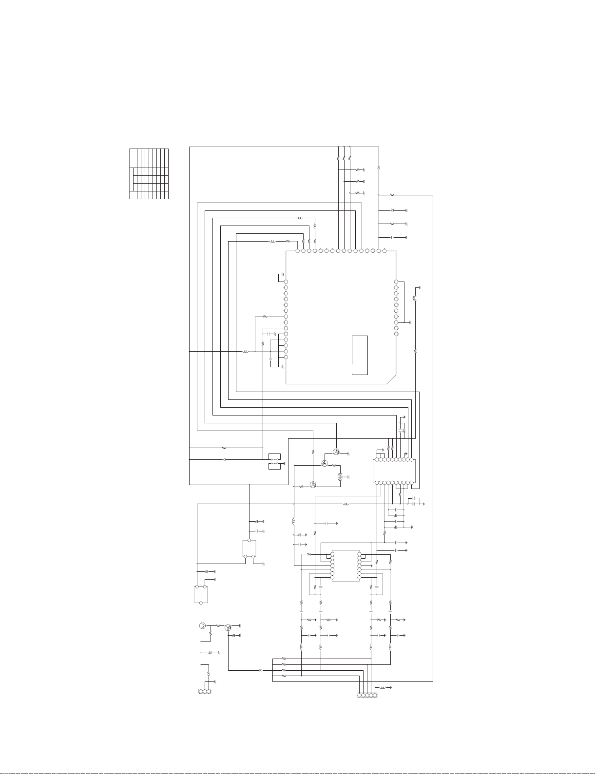
TX_SCHEMATIC
ACC75T/ACC75TK
CN103 : 16 PIN CONNECTOR
CN102 : 14 PIN CONNECTOR
CN101 : 10 PIN CONNECTOR
Note.
XHS-W759TA
BLUE LED PORT
BLUE LED PORT
BLUE LED PORT
RED LED PORT
RED LED PORT
RED LED PORT
FL-
FL+
FR-
FR+
NAME
MODEL
0000
00
00
000
00
7
6
5
4
3
2
11
1
11
1
11
11
111
ID2ID1IDO
MODEL ID
NO.
+3.3V
+3.3V
+3.3V
+3.3V
+3.3V
+5V
RESET
SDATA0
SDATA0
SDATA0
SCLK
SCLK
SCLK
LRCK
LRCK
LRCK
MCLK
MCLK
MCLK
SWITCH
RESET
SPEAKER OUTPUT
DVD RECEIVER
FROM
GND
22K
150
104
18K
22K
18K 22K
N.C
1K
1K
1K
104
1K
8.2V
DC_JACK
1SS133
101
18K
18K
101
22K
104
104
!K
101
150
104 103
104
1K1K
KTA1273
XC6203E332PR
22K
2.2K
104
22K
22K
101
1K
HB1M-102J
104
N.C
220/10
10/16
47/16
10K
1K
(DUAL LED)
SAB5370
1/50
10/16
104
KRA103S
1SS133
KRC103S
4.7M
1K
TACT_S/W
KRC103S
180
47
10K
22K
22K
2.2P
2.2P
TLC274
104
10K
2SC2412KR
104
10/16
103
10K
LG-VISION.WTR0501
10K
104
HB1M-102J
N.C
HB1M-102J
HB1M-102J
N.C
N.C
N.C
3.3V
HB1M-102J
10K
10K
10K
470
HB1M-102J
10K
104
22K
HB1M-102J
10/16
10K
10K
3.3K
HB1M-102J
HB1M-102J
XB1117P501FR
HB1M-102J
PCM1803
104
10K
10/16
HB1M-102J
4.7/16
2
1
3
GND VOUT
VIN
1
23
21
3BR
2
1
3
5
4
14
13
12
11
10
9
87
6
5
4
1
2
3
OUTPUT4
4-
4+
VEE
3+
3-
OUTPUT3
OUTPUT1
1-
1+
VCC
2+
2-
OUTPUT2
GPA8_REMOTE_CONTROLLER
GPB11/CH_ID1
GPB8/PWR_CTRL0
NO_CONNECT
GPB9/CH_ID0
GPA6/SPDIF_IN
GPA7/SPDIF_OUT
AGND
VCC33
AGND
VCC33
AGND
RESET
TDI
JTAG_RST
TMS
TCK
TDO
DGND
J39
J37
J20
J15
J36
J21
J04
J03
J02
J01
J05
J10
J11
J00
GPA0/AUD_SCLK
GPA1/AUD_LRCK
GPA2/AUD_DATA
GPA3/AUD_MCLK
GPB0/SPK_ID0
GPB1/SPK_ID1
GPB2/SPK_ID2
GPB6/LED0
GPB5/MODEL_ID2
GPB4/MODEL_ID1
GPB3/MODEL_ID0
GPB7/LED1
GPB10/PWR_SENS
J06
J07
J08
J09
J24
J25
J26
J27
J28
J29
J30
J31
J32
J33
J34
J35
EEPROM_ENB
EXT_UXTALIN
DGND
USBDPLUS
USBDMINUS
SDA
SCL
DGND
J38
J18
J14
J17
J16
J22
J23
J13
J12
J19
40 39 38 37 36 35 34 33 32 31 30 29 28 27
26
25
24
23
22
21
20
19
18
17
16
15
14
13
12
11
10
987
6
543
2
1
VIN
VOUT
GND
1
2
3
TEST
R
L
V
V
DD
BCK
DOUT
DGND
V
SCKI
OSR
FMT0
FMT1
MODE2
MODE1
LRCK
FSYNC
PDWN
AGND
V
2V
1V
CC
REF
REF
IN
IN
20
19
18
17
16
15
20
19
18
17
16
15
14
13
12
1110
9
8
7
6
5
4
3
2
1
R132
R179
C113
R143
R131
R141 R129
W102
R182
R183
R184
C112
R185
ZD101
JK101
D101
C110
R142
R144
C111
R130
C115
C114
R145
C108
R155
C165 C162
C179
R148
R147
Q102
IC101
R150
R151
C170
R136
R135
C109
R146
FB101
C120
D105
C102
C104
C103
R172
R139
LD102
C101
C119
C118
Q105
D104
Q104
R137
R109
SW101
Q101
R106
R138
R108
R134
R133
C117
C116
JK102
IC108
C131
R171
Q103
C132
C169
C161
R170
IC103
R116
C168
FB105
W103
FB102
FB111
R121
R120
R119
ZD102
FB103
R125
R127
R126
R181
FB106
R101
C133
R100
FB104
C167
R159
R158
R180
FB107
FB108
IC102
FB110
IC110
C194
R173
C164
FB109
C166

5-10
•WIRElESS PART
3. RX SCHEMATIC DIAGRAM
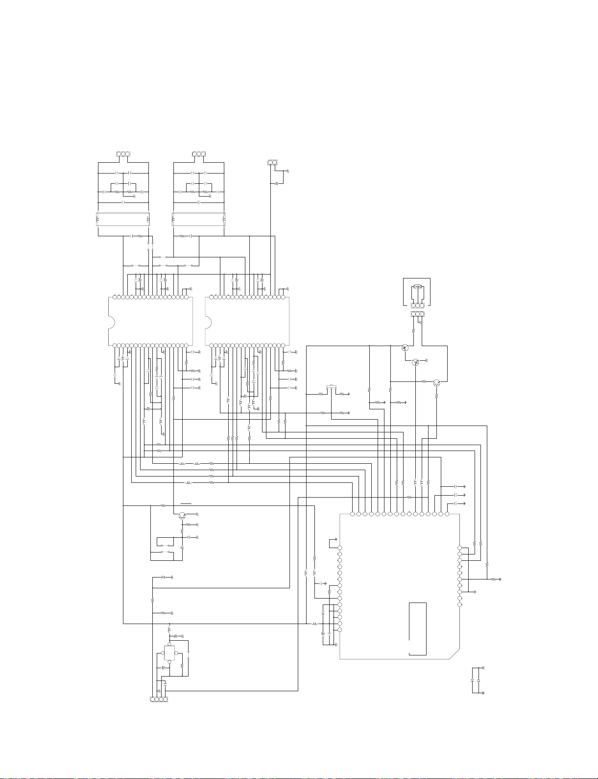
LHS-W75TA_RX
1:2_1CHANNEL_OUTPUT
LRCK
BCK
DATA0
CN211 : 16 PIN CONNECTOR
CN210 : 14 PIN CONNECTOR
CN209 : 10 PIN CONNECTOR
12.288MHz
12.288MHz
+32.5V
R_CH SPK.
L_CH SPK.
ONLY RIGHT CHANNEL CHIP
SDA1
SCL1
SDA2
SDA2
SCL2
SCL2
ST-BY ST-BY
ST-BY
P-SENS
GND
+3.3V
RED_LED
BLUE_LED
Note.
P-SENS
P-SENS
P-SENS
LED PCB
+3.3V
+3.3V +3.3V
+3.3V
+3.3V
+3.3V
RESET
SDA
SCL
+3.3V
SWITCH
RESET
GND
SPK-
SPK-
SPK+
SPK+
224
1SS133
1SS133
3.3V
N.C
104
N.C N.C 104 104
4P_2.5mm
N.C N.C
N.C
N.C
220
104
100
100
100
BEAD
N.C
N.C
BEADBEAD
BEAD
BEAD
BEAD
BEAD
N.C 20/3216
1000/50
BEAD
331
BEAD
15uH
BEAD
N.C
104(M)
104(M)
5.6
5.6
104104
N.C N.C
N.C N.C
N.C
N.C
474(M)
N.C
N.C
3-2P_3.96mm
2P_3.96mm
N.C
100/50
224
0
N.C
N.C N.C
N.C
N.C
N.C
N.C
N.C
N.C
N.C
N.C N.C
N.C N.C
100/50
N.C
BEAD
BEAD
22/16
N.C
10K
10K
3.3K
N.C
N.C
N.C
N.C
1K
3.3K
10K
N.C
N.C
Dual_LED
N.C
N.C
10
3.3K
82
104
104
272
N.C
2SC2412KR
N.C
LG-VISION.WTR0501
N.C
221
272
N.C
N.C
1SS133
10K
N.C
N.C
N.C
3.3/50
KRA103S
3P_2mm_ANGLE
100
100
100
104
104
104
104
10K
3P_2mm
104
104
N.C
N.C
N.C
2SC2412KR
10K
N.C
N.C
10K
104
104
KRC103S
STA328
470
104
2.2K
N.C
TIN_WIRE
TIN_WIRE
0
3.3V
470
100/16
100/16
TIN_WIRE
N.C
N.C
N.C
N.C
N.C
TIN_WIRE
TIN_WIRE
N.C
PIN_HEARDER
TIN_WIRE
2
1
3
4
4
32
1
2
1
3
2
1
3
2
1
GNDSUB
PLL_FILTER
SDI_12
BICLKI
LRCKI
GND3
VDD3
VREG2
VSIG
VDD3
VREG1
GND
GNDCLEAN
N.C.
GND1A
GND1B
VCC1B
VCC2A
GND2A
GND2B
N.C.
N.C.
N.C.
CONFIG
RESET
SCL
SDA
XTI
GNDA
VDDA
OUT1A
VCC1A
OUT1B
OUT2A
VCC2B
OUT2B
36
35
34
33
32
31
30
29
28
27
26
25
24
23
22
21
20
19 18
17
16
15
14
13
12
11
10
9
8
7
6
5
4
3
2
1
21
3BR
GPA8/MONO PARALLEL MODE
SDA1
SCL1
GPB11/N.C
GPB9/N.C
GPB5/N.C
GPB4/SDA2
GPB3/SCL2
GPB8/PWR_CTRL0
NO_CONNECT
GPA6/SPDIF_IN
GPA7/SPDIF_OUT
AGND
VCC33
AGND
VCC33
AGND
RESET
TDI
JTAG_RST
TMS
TCK
TDO
DGND
J39
J37
J20
J15
J36
J21
J04
J03
J02
J01
J05
J10
J11
J00
GPA0/AUD_SCLK
GPA1/AUD_LRCK
GPA2/AUD_DATA
GPA3/AUD_MCLK
GPB0/SPK_ID0
GPB1/SPK_ID1
GPB2/SPK_ID2
GPB6/LED0
GPB7/LED1
GPB10/PWR_SENS
J06
J07
J08
J09
J24
J25
J26
J27
J28
J29
J30
J31
J32
J33
J34
J35
EEPROM_ENB
EXT_UXTALIN
DGND
USBDPLUS
USBDMINUS
DGND
J38
J18
J14
J17
J16
J22
J23
J13
J12
J19
40 39 38 37 36 35 34 33 32 31 30 29 28 27
26
25
24
23
22
21
20
19
18
17
16
15
14
13
12
11
10
987
6
543
2
1
2
1
3
2
1
3
GNDSUB
PLL_FILTER
SDI_12
BICLKI
LRCKI
GND3
VDD3
VREG2
VSIG
VDD3
VREG1
GND
GNDCLEAN
N.C.
GND1A
GND1B
VCC1B
VCC2A
GND2A
GND2B
N.C.
N.C.
N.C.
CONFIG
RESET
SCL
SDA
XTI
GNDA
VDDA
OUT1A
VCC1A
OUT1B
OUT2A
VCC2B
OUT2B
36
35
34
33
32
31
30
29
28
27
26
25
24
23
22
21
20
19 18
17
16
15
14
13
12
11
10
9
8
7
6
5
4
3
2
1
4
21
3
4
32
1
C236
D277
D278
ZD202
R200
C266
C263 C262 C261 C260
CN201
FB214 FB216
FB212
FB217
R275
C225
R213
R212
R214
FB211
R209
R210
FB215FB213
FB218
FB207
FB226
FB225
C238
R228
C214
FB221
C237
FB219
L201
FB206
R231
C239
C240
R230
R229
C243C244
C246 C245
R233 R232
C242
C241
C255
C256
CN206
CN208
CN204
R291
C212
C235
R290
C281
FB204 C283
FB202
W208
W207
R294
C289
C290
IC204
R296
R295
C295
C294
C213
C291
FB201
FB203
C280
R264
R207
R283
R217
R292
R293
R282
R281
R208
R250
R280
C202
R279
LD401
C293
C292
R235
R271
R234
C250
C249
C222
R206
Q201
R260
IC201
R261
C221
C282
R252
R253
D201
R205
C286
C287
C296
C203
Q203
CN401
R258
R237
R238
C253
C254
C231
C252
R244
CN203
C233
C232
R299
C299
R278
Q205
R257
C298
C297
R249
C288
C234
Q204
IC203
R219
C257
R202
R277
W206
W205
R276
ZD201
R236
C201
C200
W202
R298
R297
W204
IC202
L202
W201
W250
R201
SW203
W203
(LD501)
(CN501)

5-12
•WIRElESS PART
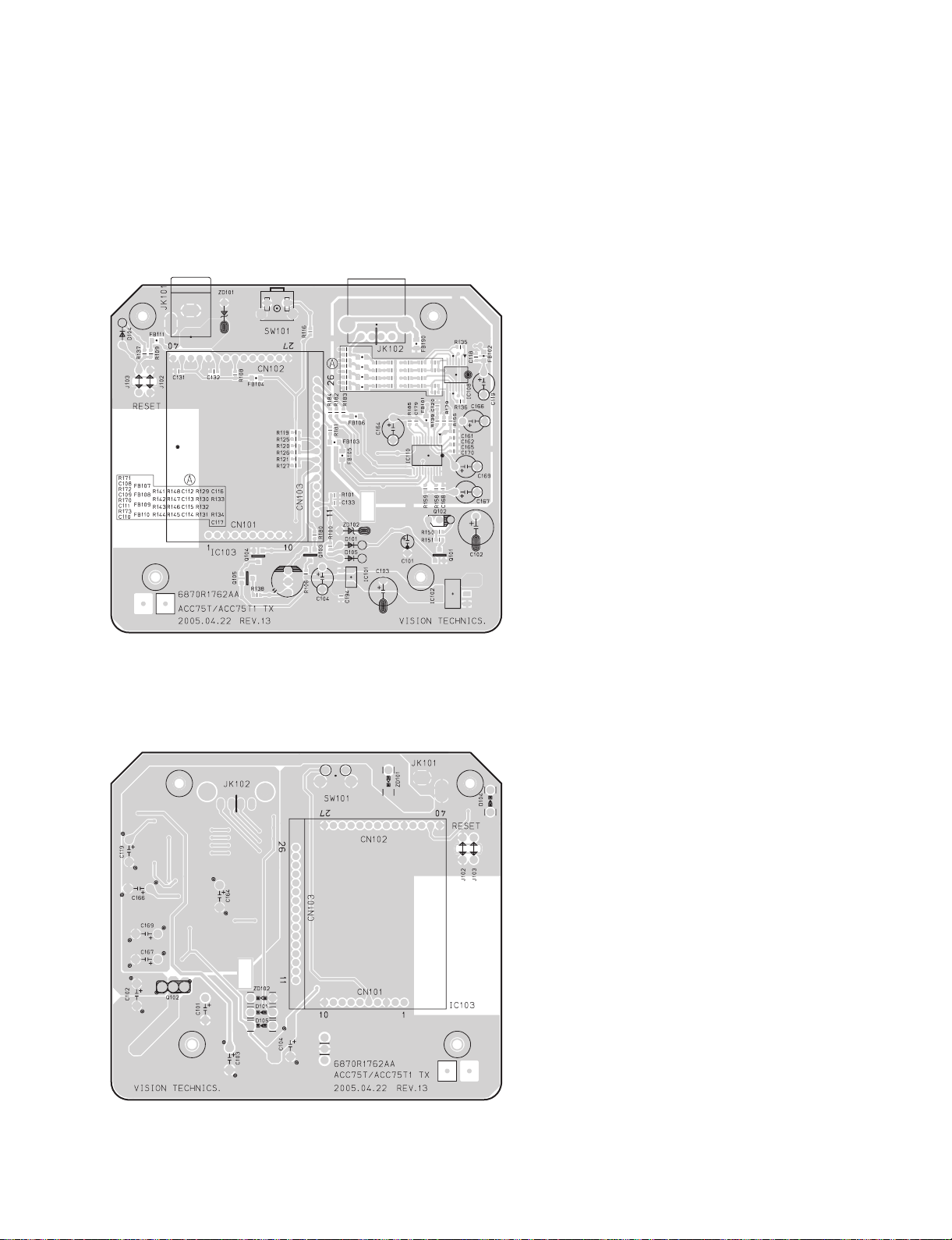
5. TX P.C. BOARD DIAGRAM
(TOP VIEW)
(BOTTOM VIEW)

5-13
•WIRElESS PART
6. RX P.C. BOARD DIAGRAM
(TOP VIEW)
(BOTTOM VIEW)

©2006 Fairchild Semiconductor Corporation
1
www.fairchildsemi.com
February 2006
FSCQ-Series Rev. 1.1.2
FSCQ-Series Green Mode Fairchild Power Switch (FPS™)
FSCQ-Series
FSCQ0565RT/FSCQ0765RT/FSCQ0965RT/FSCQ1265RT/
FSCQ1465RT/FSCQ1565RT/FSCQ1565RP
Green Mode Fairchild Power Switch (FPS™)
Features
■
Optimized for Quasi-Resonant Converter (QRC)
■
Advanced Burst-Mode Operation for under 1W
Standby Power Consumption
■
Pulse-by-Pulse Current Limit
■
Over Load Protection (OLP) – Auto Restart
■
OverVoltage Protection (OVP) – Auto Restart
■
Abnormal Over Current Protection (AOCP) – Latch
■
Internal Thermal Shutdown (TSD) – Latch
■
Under Voltage Lock Out (UVLO) with Hysteresis
■
Low Startup Current (typical: 25µA)
■
Internal High Voltage SenseFET
■
Built-in Soft Start (20ms)
■
Extended Quasi-Resonant Switching
Applications
■
CTV
■
Audio Amplifier
Related Application Notes
■
AN4146: Design Guidelines for Quasi-Resonant
Converters Using FSCQ-Series Fairchild Power
Switch.
■
AN4140:Transformer Design Consideration for
Off-Line Flyback Converters Using Fairchild Power
Switch.
Description
A Quasi-Resonant Converter (QRC) typically shows
lower EMI and higher power conversion efficiency com-
pared to conventional hard-switched converter with a
fixed switching frequency. Therefore, a QRC is well
suited for noise-sensitive applications, such as color TV
and audio. Each product in the FSCQ-Series contains an
integrated Pulse Width Modulation (PWM) controller and
a SenseFET, and is specifically designed for quasi-
resonant off-line Switch Mode Power Supplies (SMPS)
with minimal external components. The PWM controller
includes an integrated fixed frequency oscillator, under volt-
age lockout, leading edge blanking (LEB), optimized gate
driver, internal soft start, temperature-compensated pre-
cise current sources for a loop compensation, and self
protection circuitry. Compared with a discrete MOSFET
and PWM controller solution, the FSCQ-Series can
reduce total cost, component count, size, and weight, while
simultaneously increasing efficiency, productivity, and sys-
tem reliability.These devices provide a basic platform that
is well suited for cost-effective designs of quasi-resonant
switching flyback converters.
Ordering Information
YDTU: Forming Type
VDTU: Forming Type
Product Number Package Marking Code BVdss R
ds(ON)
Max.
FSCQ0565RTYDTU TO-220F-5L (Forming) CQ0565RT 650V 2.2
Ω
FSCQ0765RTYDTU TO-220F-5L (Forming) CQ0765RT 650V 1.6
Ω
FSCQ0965RTYDTU TO-220F-5L (Forming) CQ0965RT 650V 1.2
Ω
FSCQ1265RTYDTU TO-220F-5L (Forming) CQ1265RT 650V 0.9
Ω
FSCQ1465RTYDTU TO-220F-5L( Forming) CQ1465RT 650V 0.8
Ω
FSCQ1565RTYDTU TO-220F-5L (Forming) CQ1565RT 650V 0.7
Ω
FSCQ1565RPVDTU TO-3PF-7L (Forming) CQ1565RP 650V 0.7
Ω

2
www.fairchildsemi.com
FSCQ-Series Rev. 1.1.2
FSCQ-Series Green Mode Fairchild Power Switch (FPS™)
Typical Circuit
Figure 1.Typical Flyback Application
Table 1. Maximum Output Power
Notes:
1. Maximum practical continuous power in an open frame design at 50
°
C ambient.
2. 230 VAC or 100/115 VAC with doubler.
3. The junction
t
emperature can limit the
maximum output power.
Output PowerTable
3
Product
230VAC
±
15%
2
85–265VAC
Open Frame
1
Open Frame
1
FSCQ0565RT 70W 60W
FSCQ0765RT 100W 85W
FSCQ0965RT 130W 110W
FSCQ1265RT 170W 140W
FSCQ1465RT 190W 160W
FSCQ1565RT 210W 170W
FSCQ1565RP 250W 210W
VCC
GND
Drain
Sync
VO
PWM
VFB
AC
IN
FSCQ-Series

4
www.fairchildsemi.com
FSCQ-Series Rev. 1.1.2
FSCQ-Series Green Mode Fairchild Power Switch (FPS™)
Pin Configuration
Figure 3. Pin Configuration (Top View)
Pin Definitions
Pin Number Pin Name Pin Function Description
1Drain High voltage power SenseFET drain connection.
2 GND This pin is the control ground and the SenseFET source.
3Vcc This pin is the positive supply input.This pin provides internal operating current for
both start-up and steady-state operation.
4Vfb This pin is internally connected to the inverting input of the PWM comparator.
The collector of an optocoupler is typically tied to this pin. For stable operation,
a capacitor should be placed between this pin and GND. If the voltage of this
pin reaches 7.5V, the over load protection triggers
,
which results in the FPS
shutting down.
5 Sync This pin is internally connected to the sync detect comparator
for quasi-resonant
switching. In normal quasi-resonant operation, the threshold of the sync
comparator is 4.6V/2.6V.Whereas, the sync threshold is changed to 3.0V/1.8V
in an extended quasi-resonant operation.
5. Sync
4. Vfb
3. Vcc
2. GND
1. Drain
TO-220F-5L
5. Sync
4. Vfb
3. Vcc
2. GND
1. Drain
TO-3PF-7L

12-110
Package Dimensions
High Density Mounting
Type Photocoupler
LTV-817 Series
Features
Current transfer ratio
(CTR : MIN. 50% at IF5mA, VCE 5V)
High input-output isolation voltage:
(VISO : 5,000Vrms)
Compact dual-in-line package
LTV-817 : 1-channel type
LTV-827 : 2-channel type
LTV-847 : 4-channel type
UL approved (No. E113898)
TUV approved (No. R9653630)
CSA approved (No. CA91533-1)
FIMKO approved (No. 202634)
NEMKO approved (No. P98101945)
DEMKO approved (No. 307857)
SEMKO approved (No. 9832157/01-03)
VDE approved (No. 094722)
Options available :
-Leads with 0.4"(10.16mm)spacing (M Type)
-Leads bends for surface mounting(S Type)
-Tape and Reel of Type I for SMD(Add"-TA"Suffix)
-Tape and Reel of Type II for SMD(Add"-TA1"Suffix)
-VDE 0884 approvals (Add"-V"Suffix)
Applications
1. Computer terminals.
2. System appliances, measuring instruments.
3. Registers, copiers, automatic vending machines.
4. Electric home appliances such as fan heaters, etc.
5. Signal transmission between circuits of different
potentials and impedances.

1/41
STA328
May 2006
1 FEATURES
■Wide supply voltage range (10-36V)
■3 Power Output Configurations
– 2x40W + 1x80W
– 2x80W
– 1x160W
■Power SO-36 Package
■2.1 Channels of 24-Bit DDX®
■100dB SNR and Dynamic Range
■32kHz to 192kHz Input Sample Rates
■Digital Gain/Attenuation +48dB to -80dB in
0.5dB steps
■428-bit User Programmable Biquads (EQ) per
Channel
■I
2
C Control
■2-Channel I
2
S Input Data Interface
■Individual Channel and Master Gain/
Attenuation
■Individual Channel and Master Soft and Hard
Mute
■Individual Channel Volume and EQ Bypass
■Bass/Treble Tone Control
■Dual Independent Programmable Limiters/
Compressors
■Automodes™
– 32 Preset EQ Curves
– 15 Preset Crossover Settings
– Auto Volume Controlled Loudness
– 3 Preset Volume Curves
– 2 Preset Anti-Clipping Modes
– Preset Nighttime Listening Mode
– Preset TV AGC
■Input and Output Channel Mapping
■AM Noise Reduction and PWM Frequency
Shifting Modes
■Soft Volume Update and Muting
■Auto Zero Detect and Invalid Input Detect
Muting Selectable DDX® Ternary or Binary
PWM output + Variable PWM Speeds
■Selectable De-emphasis
■Post-EQ User Programmable Mix with default
2.1 Bass Management settings
■Variable Max Power Correction for lower full-
power THD
■4 Output Routing Configurations
■Selectable Clock Input Ratio
■96kHz Internal Processing Sample Rate, 24 to
28-bit precision
■QXpander
■Video Application: 576 fs input mode suporting
2 DESCRIPTION
The STA328 is an integrated solution of digital au-
dio processing, digital amplifier control, and DDX-
Power Output Stage, thereby creating a high-pow-
er single-chip DDX® solution comprising of high-
quality, high-efficiency, all digital amplification.
The STA328 power section consists of four inde-
pendent half-bridges. These can be configured via
digital control to operate in different modes. 2.1
channels can be provided by two half-bridges and
a single full-bridge, providing up to 2x40W +
1x80W of power output. 2 Channels can be provid-
ed by two full-bridges, providing up to 2x80W of
power. The IC can also be configured as a single
paralelled full-bridge capable of high-current oper-
ation and 1x160W output.
Also provided in the STA328 are a full assortment
of digital processing features. This includes up to
4 programmable 28-bit biquads (EQ) per channel,
2.1 HIGH EFFICIENCY
DIGITAL AUDIO SYSTEM
Rev. 3
Fi
gure 1.
P
ac
k
age
Table 1. Order Codes
Part Number Package
STA328 PowerSO36 (Slug Up)
STA32813TR Tape & Reel
PowerSO36 SLUG UP

STA328
2/41
and bass/treble tone control. Automodes™ enable a time-to-market advantage by substantially reducing
the amount of software development needed for certain functions. This includes Auto Volume loudness,
preset volume curves, preset EQ settings, etc. New advanced AM radio inerference reduction modes.
The serial audio data input interface accepts all possible formats, including the popular I
2
S format.
Three channels of DDX® processing are provided. This high quality conversion from PCM audio to DDX's
patented tri-state PWM switching waveform provides over 100dB SNR and dynamic range.
3 ORDERING INFORMATION
Figure 2. Block Diagram
Figure 3. Channel Signal Flow Diagram through the Digital Core
3.1 EQ Processing
Two channels of input data (re-sampled if necessary) at 96 kHz are provided to the EQ processing block.
In this block, upto 4 user-defined Biquads can be appplied to each of the two channels.
Pre-scaling, dc-blocking high-pass, de-emphasis, bass, and tone control filters can also be applied based
on various configuration parameter settings.
The entire EQ block can be bypassed for all channels simulatneously by setting the DSPB bit to '1'. And
the CxEQBP bits can be used to bypass the EQ functionality on a per channel basis. Figure below shows
the internal signal flow through the EQ block.
Serial Data
Input,
Channel
Mapping &
Resampling
DDX®
Processing
Quad
Half-Bridge
Power Stage
OUT1A
OUT1B
OUT2A
OUT2B
LRCKI
SDI_12
SDA SCL
PLL
CLK
EAPD
BICKI
FAULTTWARN
Power-Down
I2C
System Contro
l
Audio EQ, Mix,
Crossver,
Volume, Limiter
Processing
System Timing
DDX-SPIRIT
Serial Data
Input,
Channel
Mapping &
Resampling
DDX®
Processing
Quad
Half-Bridge
Power Stage
OUT1A
OUT1B
OUT2A
OUT2B
LRCKI
SDI_12
SDA SCL
PLL
CLK
EAPD
BICKI
FAULTTWARN
Power-Down
I2C
System Contro
l
Audio EQ, Mix,
Crossver,
Volume, Limiter
Processing
System Timing
DDX-SPIRIT
Channel
Mapping Re-s amp ling EQ
Processing Mix Volume
Limiter
4X
Interp DDX
®
I
2
S
Input
DDX
Output
Crossover
Filter

3/41
STA328
Figure 4. Channel Signal Flow through the EQ Block
Figure 5. 2-Channel (Full-bridge) Power, OCFG(1…0) = 00
Figure 6. - 2.1-Channel Power Configuration OCFG(1…0) = 01
Figure 7. 1-Channel Mono-Parallel Configuration, OCFG(1…0) = 11
Pre
Scale
High-Pass
Filt er BQ#1 BQ#2 Bass
Filt er
De-
Emphasis
Treble
Filter
Re-sampled
Input
To
Mix
BQ#4BQ#3
If HPB = 0
4 Biquads
User defined if AMEQ = 00
Preset EQ if AMEQ = 01
Aut o L oudn ess if AM EQ = 1 0
If DEMP = 1
If CxT CB = 0
BT C: Bass Bo o st /Cut
TTC: Treble Boost/Cut
If DSPB = 0 & CxEQB = 0
Half
Bridge
Half
Bridge
Half
Bridge
Half
Bridge
OUT1A
OUT1B
OUT2A
OUT2B
Channel 2
Channel 1
Half
Bridge
Half
Bridge
Half
Bridge
Half
Bridge
OUT1A
OUT1B
OUT2A
OUT2B
Channel 2
Channel 1
Half
Bridge
Half
Bridge
Half
Bridge
Half
Bridge
OUT1A
OUT1B
OUT2A
OUT2B
Channel 3
Channel 1
Channel 2
Half
Bridge
Half
Bridge
Half
Bridge
Half
Bridge
OUT1A
OUT1B
OUT2A
OUT2B
Channel 3

STA328
4/41
Figure 8. Block Diagram (refer to Stereo Application Circuit)
Figure 9. Pin Connection
L18 22µH
L19 22µH
C30
100nF
C20
100nF
C99
100nF
C101
100nF
C107
100nF
C106
100nF
C23
470nF
C55
1000µF
C21
100nF
R63
20
R98
6
R100
6
C31
1µF
C52
330pF
R104
20
20pF
15
M3
Vcc Sign
V
L
SCL
SDA
RESET
BICKI
SDI
LRCKI
XTI
3.3V
3.3V
GND REG
CONFIG
V
SS
V
DD REG
VDDA
GNDA
REGULATORS
PROTECTION
&
LOGIC
DIGITAL
PWM
MODULATOR
19
35
36
18
20
21
17
24
23
M2
M5
M4
16
OUT1A
V
CC
1A
11
10
GND1B
OUT1B
V
CC
1B
12
L113 22µH
L112 22µH
C32
100nF
+V
CC
C108
470nF
C33
1µF
8
M17
M15
M16
M14
9
OUT2A
V
CC
2A
4
3
GND2B
D00AU1541
OUT2B
V
CC
2B
6
32
22
30
26
31
27
33 1, 2, 5, 14,
GNDCLEAN
34
28
29
C110
100nF
C111
100nF
R103
6
R102
6
VDD
GND
N.C.
7250
550pF
25
RES
7
13 GND1A
GND2A
3.3V
N.C.
N.C.
OUT2B
V
CC
2B
GND1A.
V
CC
1A
N.C.
OUT1A
GNDCLEANVL
CONFIG
RESET
SDA
SCL
GND
VDD
V
SS
V
CC
Sign
18
16
17
15
6
5
4
3
2
21
22
31
32
33
35
34
36
20
1
19 GND REGVDD REG
D04AU1540
OUT1B
GND1B
V
CC
1B
RES
XTI
PLL FILTER
9
8
7
28
29
30
OUT2AGNDA
1027
N.C.
V
CC
2A
GND2A
VDDA
BICKI
SDI
14
12
11
23
25
26
GND2BLRCKI
1324

Other manuals for LH-W750TA
2
This manual suits for next models
9
Table of contents
Other LG Receiver manuals