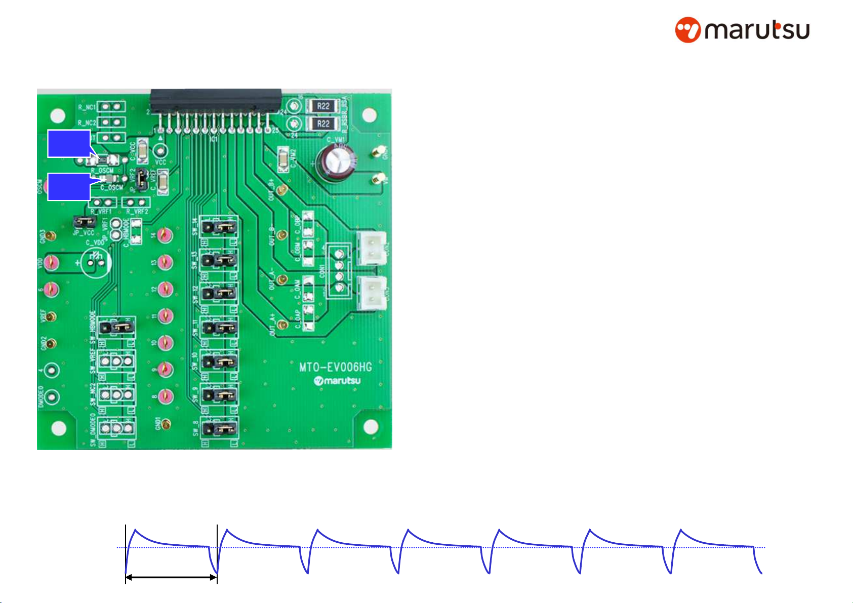
Connection of Evaluation Board 2
In use of Large Mode
③
③③
③
①
①①
①
④
④④
④
②
②②
②
⑤
⑤⑤
⑤
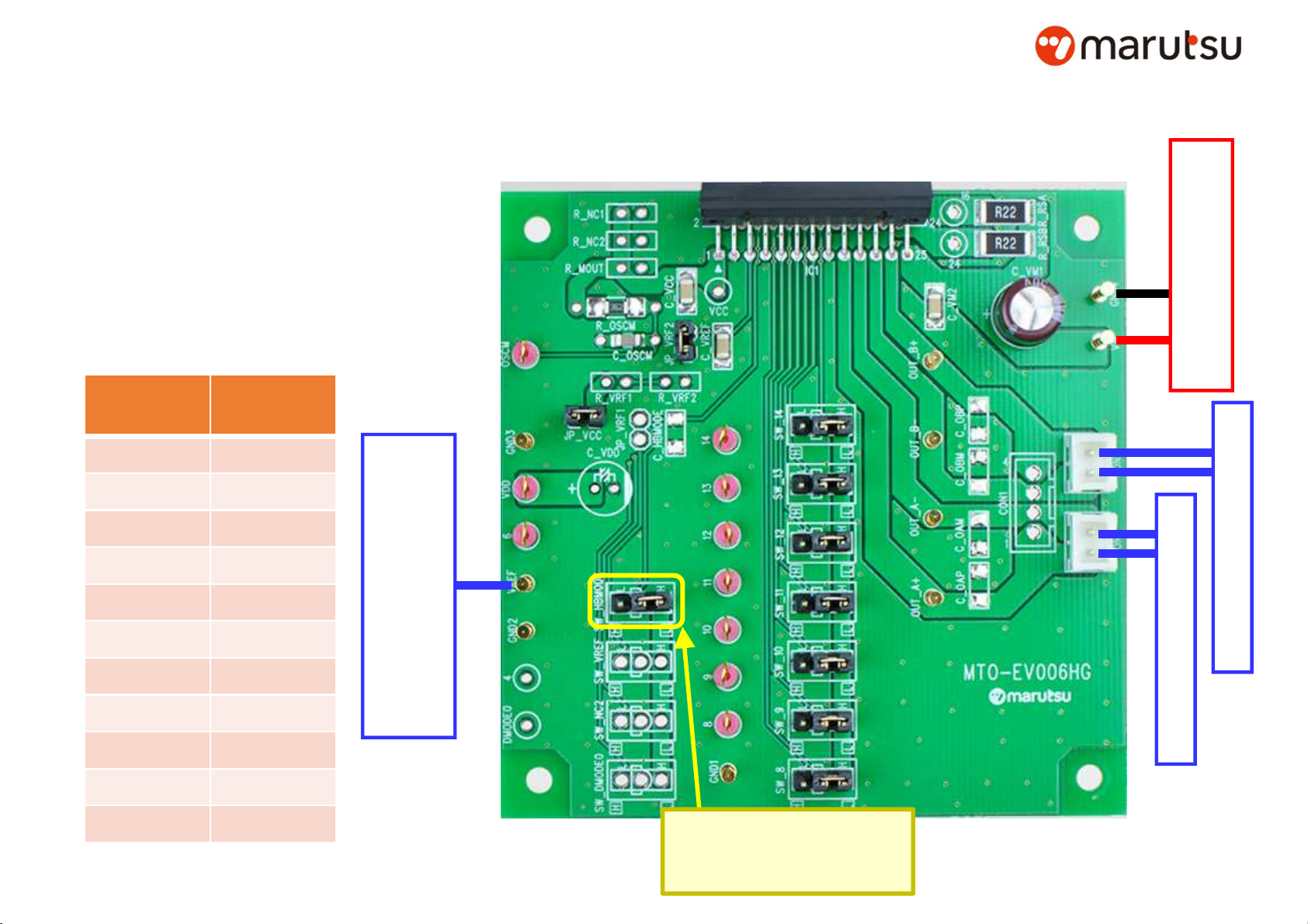
HBMODE
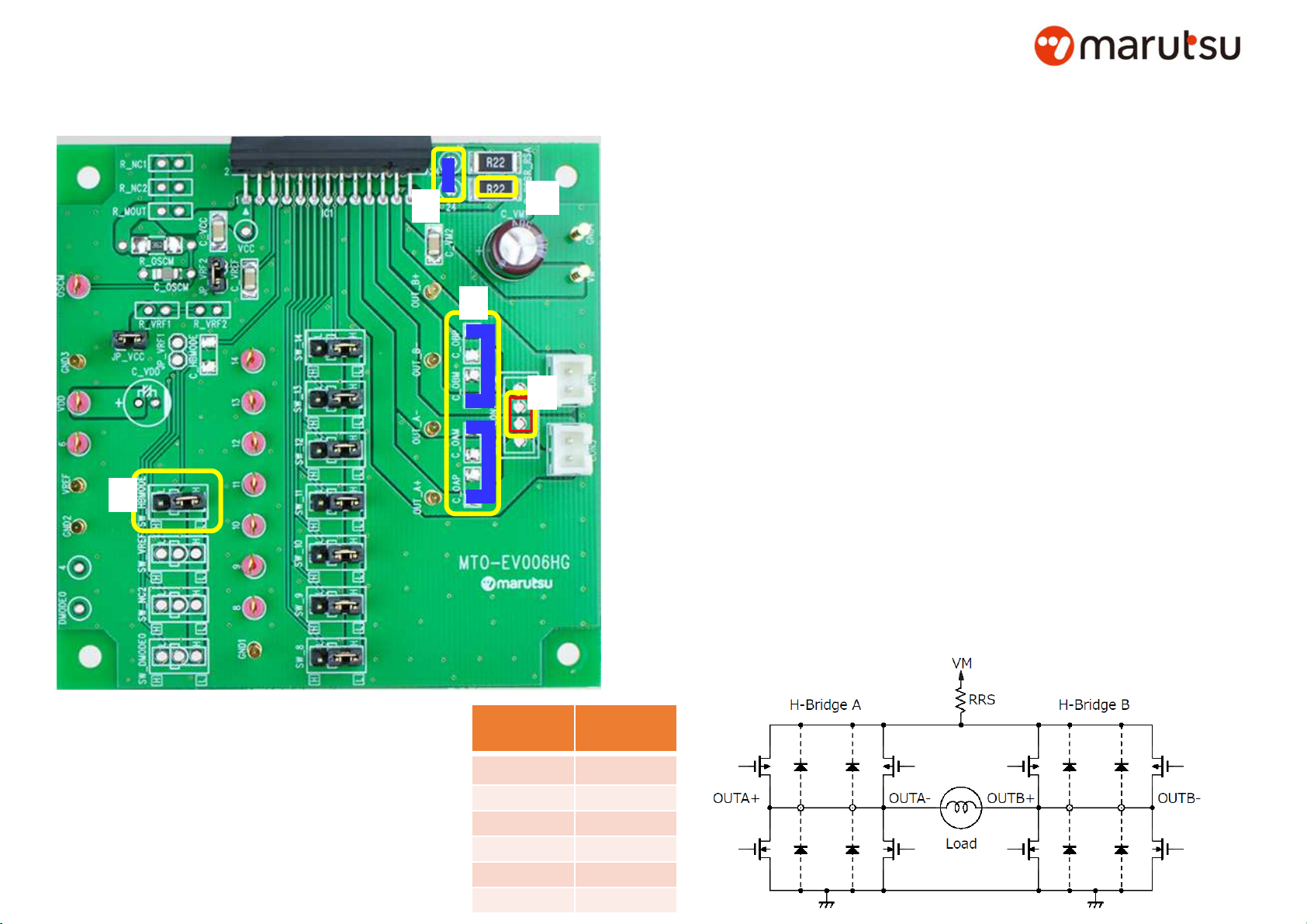
Large Mode is a parallel control function of the output
part, OUTA+ and OUTA-, OUTB+ and OUTB- are tied
in cascade as shown in the circuit diagram below.
n that case, the current balance of A-ch and B-ch
becomes important in operation due to high current.
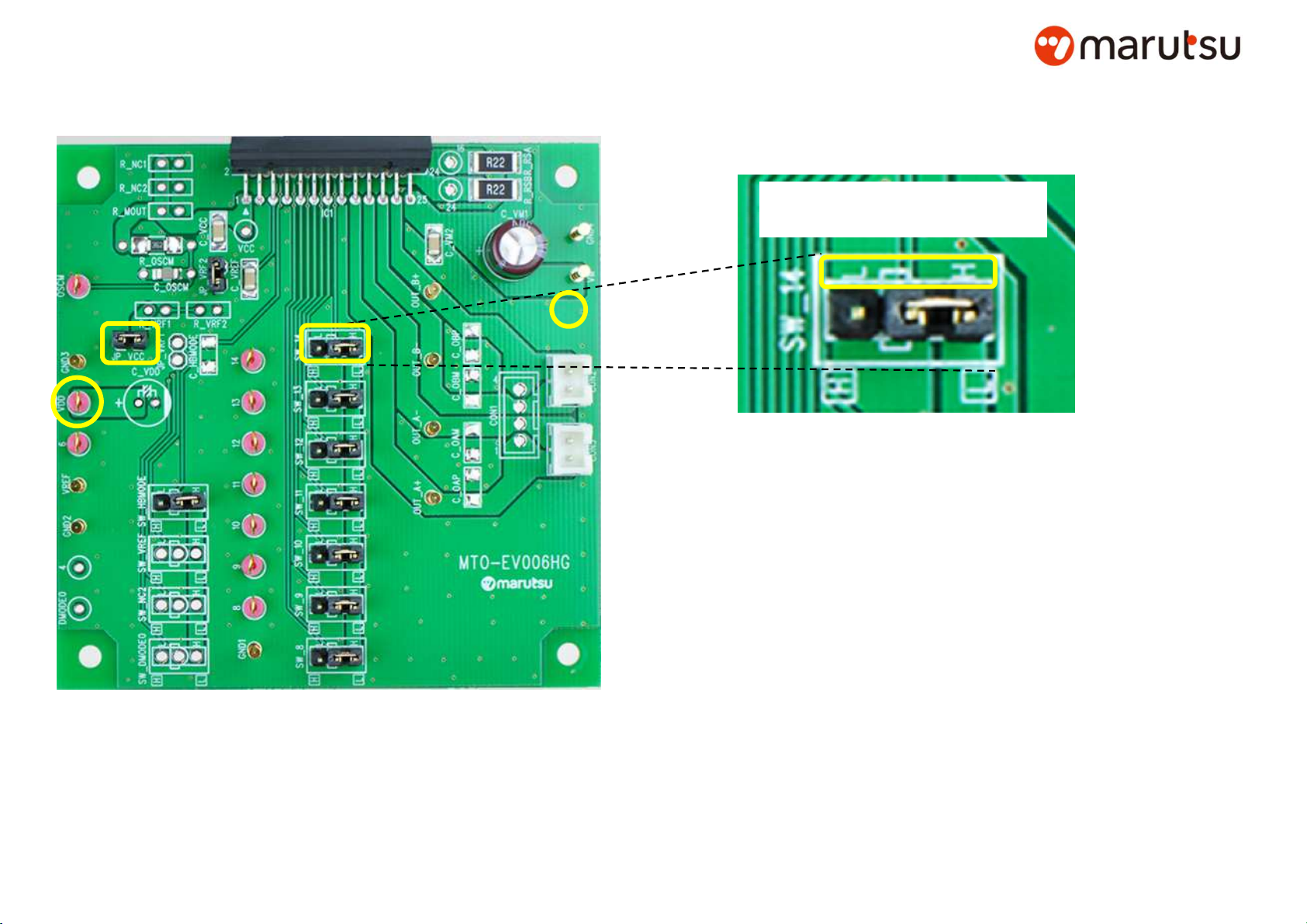
n use of this mode please make the following changes.
①Mounting the motor connector
Please mount a connector at the two pins in the middle.
②Shorting of RSA terminal and RSB terminal
By using the holes for check pin mounting, RSA terminal and
RSB terminal are shorted with wiring.
Mounting of 0 Ω resistor (short resistor)
To commonize RSS, by utilizing the rounds for C_OAM, C_OAP
and C_OBM, C_OBP, OUTA+ and OUTA-, OUTB- and OUTB+
are shorted with wiring etc.
④Removal of resistor R_RSB
The resistor R_RSA becomes RRS in the circuit diagram below.
The constant current control value is set according to the input
voltage Vref.
⑤Set HBMODE to "H" level
In order to input "H“ level, please set a short pin to "H“ side.
【Changed unction of Terminal 】
n Large Mode, the functions of
each terminal are changed as
shown in the table on the right.
Silk
name
Signal
name
8 IN1
9 IN2
10 PWM
11 Non use
12 Non use
13 Non use 1 Large DC Motor operation
A-ch and B-ch are connected
in parallel to form one H-Bridge,
and it drives one motor.