Basic N tes in Using Evaluati n B ard
P wer supply v ltage and perating v ltage range
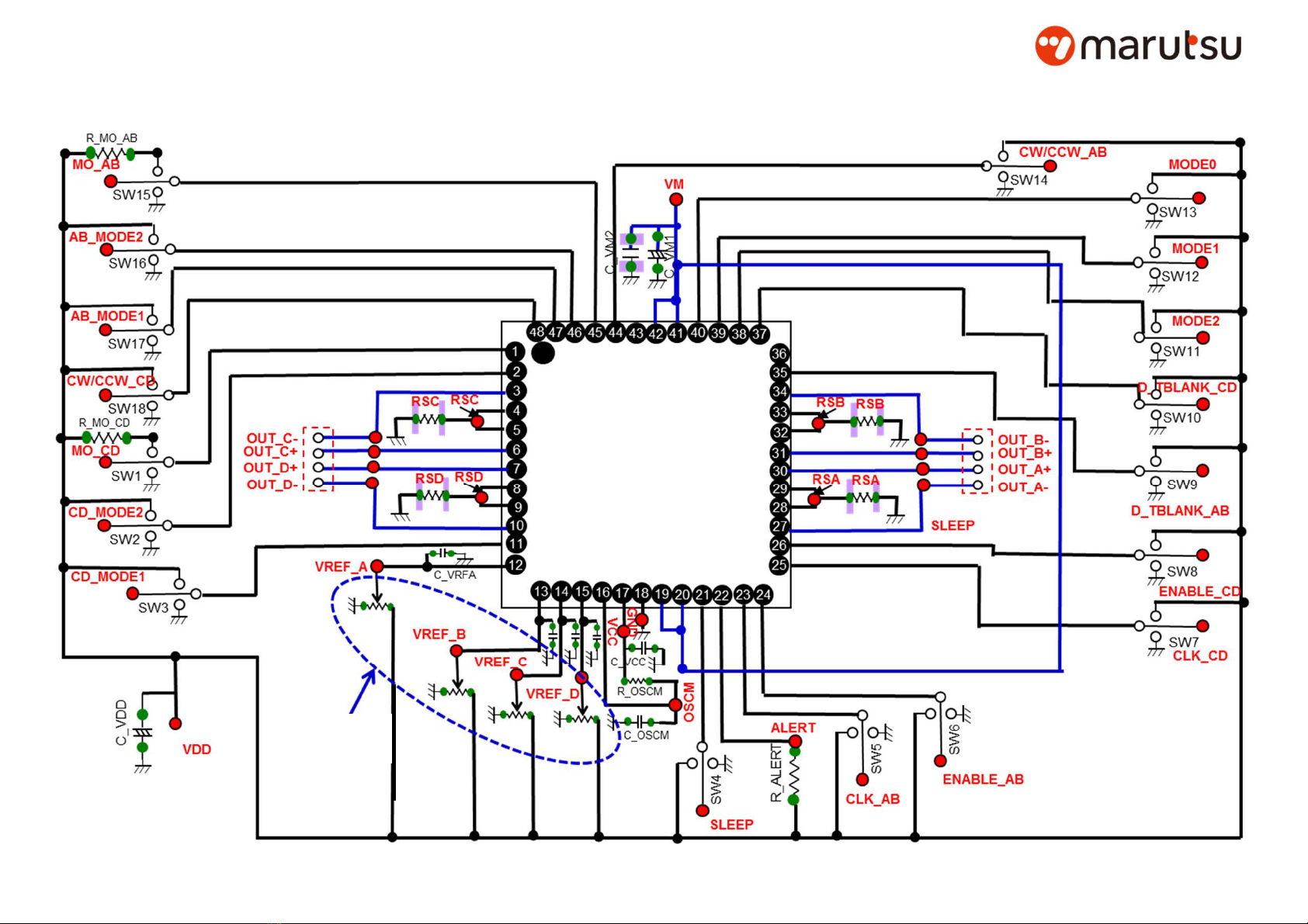
Apply the v ltage t the VM pin in evaluating the IC.
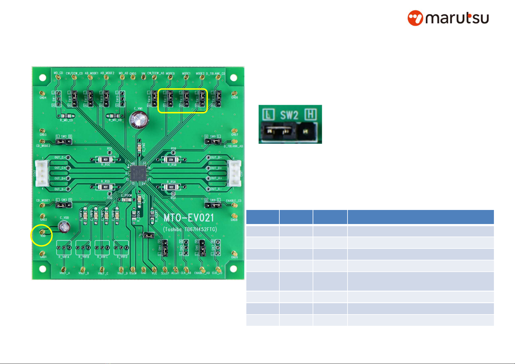
In case f using the level select pin m unted n this evaluati n b ard, the v ltage sh uld be applied t the
VDD pin.
Th ugh the abs lute maximum rating f the VM p wer supply v ltage is +40 V, evaluate the IC within the
rated perating range f +6.3 V t 38.0 V.
The VDD v ltage sh uld be within the l gic input v ltage range f +3.3 V t 5.0 V in using the level select pin.
P wer n and ff sequence
There are n special pr cedures in applying a p wer supply and shutd wn since the IC implements the under
v ltage detecti n circuit (UVLO).
H wever, it is rec mmended t turn ff the m t r perati n during the p wer n and the shutd wn where
the VM v ltage is unstable. Start the m t r perati n by switching the input signals after the p wer supply
v ltage bec mes stable.
Output current
M t r current sh uld be 2.0 A r less that c rresp nds t the perating range.
H wever, the maximum current f the actual usage is limited depending n the usage c nditi ns (the ambient
temperature, the radiati n path, the exciting design, etc.). C nfigure the m st appr priate current value after
calculating the heat and evaluating the b ard under the perating envir nment.
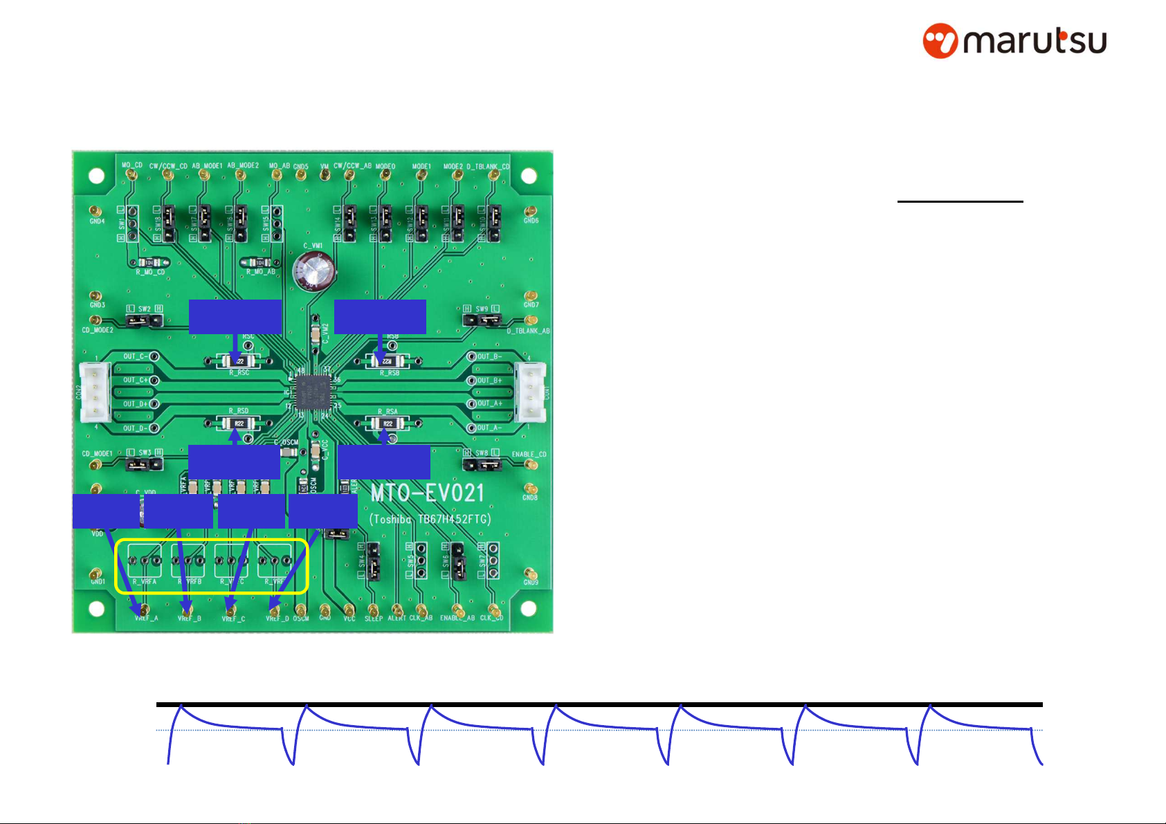
C ntr l input
It is rec mmended t c nfigure the input signals f ENABLE_AB, ENABLE_CD, AB_MODE1, AB_MODE2,
CD_MODE1, CD_MODE2, CLK_AB and CLK_CD t l w level while the VM v ltage is n t supplied.
When the l gic signal is input with ut the VM v ltage supply, the electr m tive f rce is n t generated.