Megatel Quark/100 User manual
THE
MEGATEL
QUARK~100
SINGLE
BOARD
COMPUTER
ENTIRE
CONTENTS
COPYRIGHT
MEGATEL
COMPUTER
TECHNOLOGIES
150
TURBINE
DRIVE
WESTON,
ONTARIO,
CANADA
M9L
2S2
MA-223010-RO
TABLE
OF
CONTENTS
HARDWARE
Introduction to the
QUARK
famiLy
of singLe
board
computers
Recommended
drives for the
MegateL
QUARK
Recommended
monitors for the
MegateL
QUARK
Recommended
keyboards for the
QUARK
Required
power
suppLy
for the
QUARK
MegateL
QUARK
CPU
Overview
CPU
Memory
Management
QUARK
Boot
Mode
Memory
Mapping
QUARK
Video
DispLay
Memory
Programming
the
SAM
Registers
QUARK
Interrupt
System
The
QUARK
Video
DispLay
Interfaces
Video
DispLay
Memory
ALphanumeric
Mode
Bit-mapped
Graphics
Mode
Loading
the
Programmable
Character Generator
PeripheraL Interfaces
ParaLleL
Printer Interface
ParaLLel
Keyboard
Interface
Full-Duplex
Serial
Interface
Simplex
Serial
Interface
Parallel
I/O
lines
Serial
Keyboard
Interface
Special I/O Functions
Floppy
Disk
Interface
Expansion
of the
Megatel
QUARK
MisceLlaneous
hardware
notes for the
QUARK
SOFTWARE
Software for the
QUARK
The
QUARK
Operating
System
The
Megatel
QUARK
Software
Package
CP/M
Commands
and
Utilities
Megatel
Utilities
and
Files
CP/M
Users'
Group
Utilities
Installing
the
Customized
CP/M
System
Operation of a one-drive
system
Temporary
enabling of the
second
drive
on
a two-drive
system
Formatting diskettes to
make
copies
Making
backup
copies of the Distribution Diskettes
Running
the
QINSTALL
procedure
Selection
"A"-Disk
drive
hardware
specifications
Selection ''S''-Diskette formatting specifications
Selection "C"-other peripherals configuration
Final steps in the
Installation
procedure
New
disk format
and
new
CP/M
system
HIW
PAGE
MIllER
1
1
1
~~
3
3
5
6
7
7
9
10
11
12
14
15
15
15
16
17
19
20
21
21
22
23
SIW
PAGE
tIllER
1
2
4
4
6
8
9
9
10
10
11
12
13
~~
--,?
19 -
-z.,/
19
__
2-2--

SOFTWARE
Formatting a
diskette
under
the
new
format
Writing the
new
system
on
a
diskette
Booting the
new
system
Transferring
files
from
the
Work
Diskette
Mixed
Drive
Installations
QCERT.COM-The
diskette
formatting
utility
Operation of
QCERT
Standard
diskette
format
QCERT
error
messages
QCERT
parameters
Interlace
Tables
QSYSGEN.COM-The
System
Generation
Utility
Standard
Disk
format
Configuration of
CPIM
Modules
QSYSGEN
Parameters
Parameters for the
Source
and
Destination Drives
Parameters for the
Source
Drive
only
Parameters for the Destination Drive only
Translate Tables
QSYSGEN
Parameter
Summary
D
pc
GA.
, c·uv"1
Software for the
Video
DispLay
Interface
CHRLD.COM-The
Character Generator
Loader
CHRED.COM-The
Character Set Editor
GRFLD.COM
-
The
Graphics
Mode
alphanumeric video utiLity
Loading
a Character Set other than the default for
GRFLD
Changing
the default
Graphics-mode
Character Set
QTCONFIG.COM
-Terminal
Code
Configuration UtiLity
Floppy
disk interface error
messages
APPENDIX
ELectrical Specifications
Table I
Table
II
Table
III
Table
IV
Table V
Table
VI
Table
VII
Table VIII
Table
IX
Table X
-
1/0
Addresses
and
functions for the
QUARK
64K
SBC
-Timer-1
Baud
Rates
for Full-Duplex Interface
-Timer-2
Baud
Rates for Full-Duplex Receiver in
in SpLit
Baud
Mode
-Simplex Serial Port
Baud
Rate
Selection
-Synchronous
Address
Multiplexer
Address
Assignments
-Suggested
Values
for the
Sam
Control Register
-Quark
Pin Connections
and
Functions
-Quark
Peripheral Connections
-Jumper Options
-TerminaL
ControL
Codes
SlY
PAGE
MIllER
.-
~~~
29
30
30
30
~l
)
33 /
~r;
Z-~
34
~K
1[r
37
38
APPEN>IX
PAGE
tUl3ER
1
2
4
6
7
8
9
9
12
15
16
----------------,
Limited
Warranty
----------------------------
All products sold (including software) are under
LIMITED
WARRANTY
on
a return
to
factory
basis against defects in
workmanship
and
material for a period of
90
days
from
the date of
shipment.
WARRANTY
is
contingent
l4'on
proper
use
of
the Product.
WARRANTY
will
not
app
ly
if
any
repairs are necessary
due
to accident,
unusuaL
physicaL,
electrical
or eLectro-magnetic
stress,
neglect,
misuse,
or
causes
other
than
ordinary
use.
WARRANTY
wiLL
aLso not
appLy
if
the
product has been modified
by
BUYER,
or
if
the
product has been
disassembled
by
BUYER.
Disassembly
incLudes
the
removal
of the seriaL
number
labeL
on
the Product without
prior
written
approvaL
from
MEGATEL.
Customer
attempted repairs
wiLL
void the
WARRANTY.
Any
tips
suggested in the
manual
which
involve physical
changes
to the
board
or a reconfiguration of the software,
if
attempted,
will
void the
WARRANTY.
Copyright Notice
and
Trademarks
----,---
No
part of
this
document
may
be copied or reproduced in
any
form
or
by
any
means
without
the prior written consent
of
Megatel
Computer
TechnoLogies.
Entire contents copyright Megatel
Computer
Technologies, Toronto,
Canada
1985.
Printed in
Canada.
"MegateL
Quark"
is
a registered
Canadian
trademark of
Megatel
Computer
TechnoLogies.
"CP/M"
is a registered trademark of Digital Research, Inc.
"DigitaL Research",
"CP/M
Plus",
"DDT",
"LIB-80",
"LINK-80",
"ASM",
"MAC",
"MP/M
II",
"RMAC",
and
"SID"
are registered trademarks of Digital Research, Inc.
"Microsoft"
is
a registered trademark
of
Microsoft Corporation.
"ZSO"
is a registered trademark of Zilog Inc.
"PAL"
is
a registered trademark of
MonoLithic
Memories
Inc.
"Apple"
and
"AppLe
III"
are registered trademarks of
Apple
Computer
Inc.
"Corvus
OMNINET"
is
a trademark
of
Corvus
Systems, Inc.
"IBM"
is
a tradename of InternationaL Business Machines, Inc.
"Centronics"
is
a registered trademark of Centroni
cs
Data
Computer
Corporation.
Disclaimer
MegateL
makes
no
representations
nor
warranties with respect
to
any
circuitry
not
embodied
within
a
MegateL
product.
MegateL
specifically
disclaims
any
implied
warranties
of
merchantability or
fitness
for
any
particular
purpose of
any
Megatel product.
MegateL
assumes
no
responsibility for errors
which
may
appear in
this
document,
and
reserves the right to
revise
this
document
without notice.
-------
Service Information
.
Should
a
QUARK
board
require service please contact the Megatel Engineering
office
at
416-
745-7214
for
instructions.
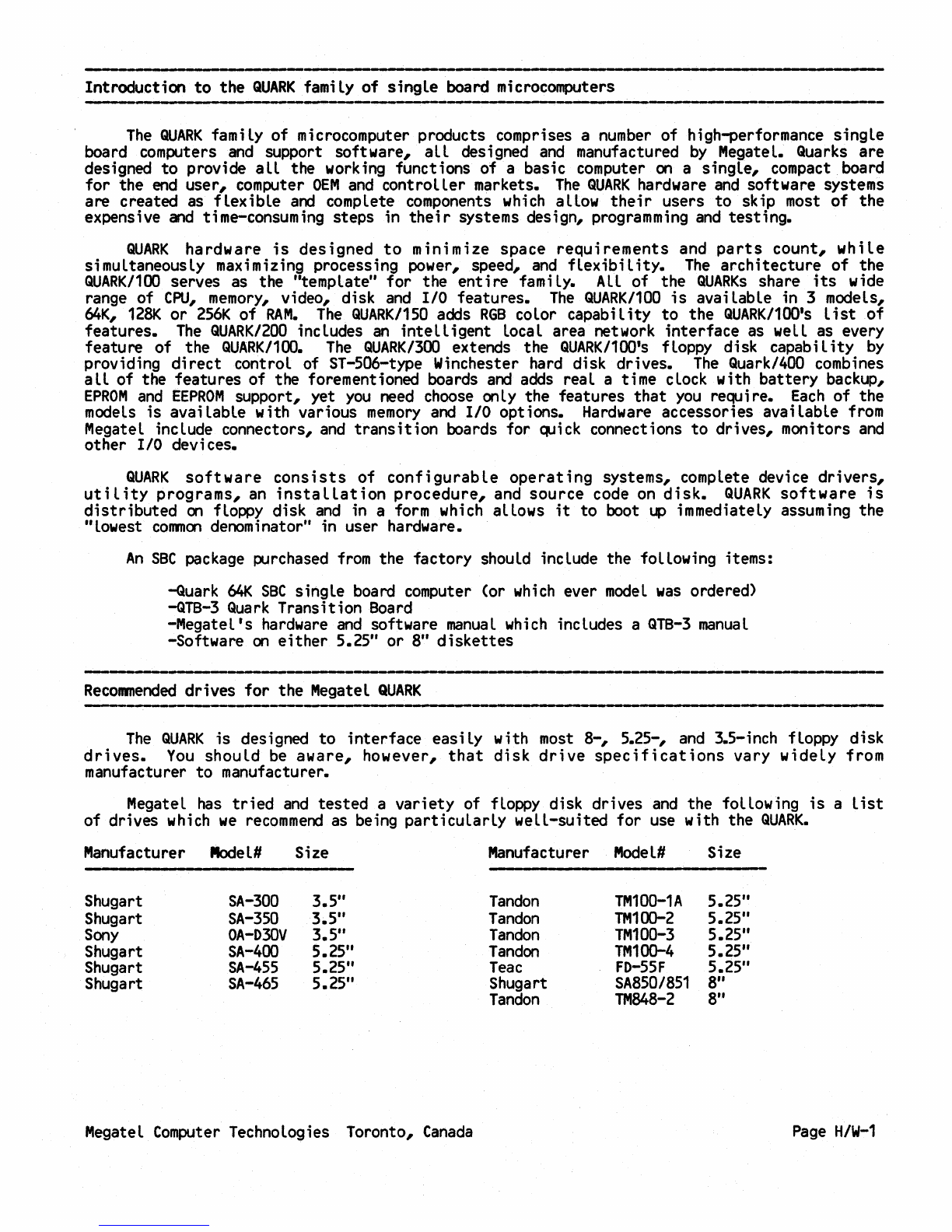
Introduction
to
the
QUARK
family of single board microcomputers
The
QUARK
family of microcomputer products comprises a
number
of high-performance single
board computers
and
support software,
all
designed
and
manufactured
by
Megatel.
Quarks
are
designed
to
provide aII the
work
ing
funct ions of a basic
computer
on
a single,
compact
board
for the
end
user,
computer
OEM
and
controller markets.
The
QUARK
hardware
and
software systems
are created
as
flexible
and
complete
components
which
allow
their
users to skip
most
of the
expensive
and
time-consuming steps
in
their
systems design,
programming
and
testing.
QUARK
hardware
is
designed
to
minimize space requirements
and
parts
count, while
si
multaneously maximizing processing power, speed,
and
flexibi l
ity.
The
architecture of the
QUARK/100
serves
as
the "template" for the enti
re
fami
LYe
ALL
of the
QUARKs
share
its
wide
range of
CPU,
memory,
video, disk
and
I/O features.
The
QUARK/100
is
avai lable
in
3 models,
64K,
1281<
or
2S6K
of
RAM.
The
QUARK/1S0
adds
RGB
color
capabi
l
ity
to
the
QUARK/100's
list
of
features.
The
QUARK/200
includes
an
intelligent
local area network interface
as
weLL
as every
feature of the
QUARK/100.
The
QUARK/300
extends the
QUARK/100's
floppy disk capabi l
ity
by
providing
direct
control
of
ST-S06-type Winchester
hard
disk drives.
The
Quark/400
combines
all
of the features of the forementioned boards
and
adds
real a time clock with battery backup,
EPROM
and
EEPROM
support, yet
you
need
choose
onLy
the features that
you
require.
Each
of the
models
is available with various
memory
and
I/O options.
Hardware
accessories available
from
Megatel
include connectors,
and
transition
boards for quick connections
to
drives, monitors
and
other
I/O
devi ces.
QUARK
software
consists
of
configurable
operating
systems,
compLete
device
drivers,
utiLity
programs,
an
instaLLation
procedure,
and
source code
on
disk.
QUARK
software
is
distributed
on
fLoppy
disk
and
in
a
form
which
aLLows
it
to
boot
up
immediateLy
assuming the
"lowest
common
denominator"
in
user hardware.
An
SBC
package
purchased
from
the factory
shouLd
include the
foLLowing
items:
-Quark
64K
SBC
single board
computer
(or
which
ever
modeL
was
ordered)
-GTB-3
Quark
Transition
Board
-Megatel's
hardware
and
software
manual
which
includes a
QTB-3
manual
-Software
on
either
5.25" or
8"
diskettes
------.------------------------------------------.--------------------------------
Recommended
drives for the
Megatel
QUARK
The
QUARK
is designed
to
interface easi
ly
with
most
8-,
5.25-,
and
3.S-inch floppy disk
drives.
You
shouLd
be
aware, however,
that
disk
drive
specifications
vary widely from
manufacturer to manufacturer.
Megatel
has
tried
and
tested a variety of floppy disk drives
and
the
foLLowing
is
a
list
of drives
which
we
recommend
as
being particularLy well-suited for
use
with the
QUARK.
Manufacturer
Model#
Size Manufacturer
Model#
Size
Shugart
SA-300
3.5"
Tandon
TM100-1A
5.25"
Shugart
SA-3S0
3.5"
Tandon
TM1(x)-2
5.25"
Sony
OA-D30V
3.5"
Tandon
TM100-3
5.25"
Shugart
SA-400
5.25"
Tandon
TM100-4
5.25"
Shugart
SA-4SS
5.25"
Teac
FD-S5F
5.25"
Shugart
SA-46S
5.25" Shugart
SA8S0/8S1
8"
Tandon
TM848-2
8"
Megatel
Computer
Technologies Toronto,
Canada
Page
H/W-1
On
the
QTB-3
there
is
a 34-pin header denoted
by
J3. A standard
5.25
inch floppy disk
cable
will
plug into
this
board in
this
area
and
connect
directly
to
the
edge
connectors of
your
floppy disk drives. This
same
34-pin header
is
used
for connecting 8 inch drives. This
can
be
done
by
taking a regular
50
pin ribbon cable
and
replacing the 50-pin female header with
a
34-pin
female header.
Strip
away
lines
48
through
50
and 1 through 13
to
give
you
the
required
34
position cable. Either set of cable
can
be
purchased
from
Megatel.
To
allow a
mixed
5.25
and
8 inch system Megatel
can
supply a cable
which
provides both a
34-pin
and
a 50-pin connector.
Assembl
ing
your
own
mixed
drive cable, although possible,
is
difficult
due
to the difference between 8
and
5.25
inch
drive interfaces.
The
next
step,
for
a mixed
drive
system,
is
to
wire wrap from
the
floppy
disk
data
transfer
rate
(pin 8-17
on
the 96-pin
DIN
connector)
to
the drive
select
line
(see appendix
for
pinout)
you
have
chosen
for
your
8 inch drive. This allows the data
transfer
rate
to
switch
automatically with drive
selection.
Notes
regarding
Floppy
Disk
Drives:
Megatel
Quarks
do
not
provide a
MOTOR
ON
signal.
Most
5.25
inch drives
wi
II
provide a
jumper
option
on
the drive
motor
control board to
have
the
motor
come
on
with the
selection
of
the drive. Please consult
your
drive
manual
to insure
this
is
done
before
you
try
to
boot up
the system.
Some
5.25 inch
drives
have a
READY
signaL.
If
you
are
using such a
drive,
you
must
isolate
the
READY
line in a
mixed
drive
installation.
If
you
are using
an
8
and
5.25
inch
drive system the
READY
line should
be
taken
directly
from
the
QTB-3
to
the 8 inch drive, while
bypassing the
5.25
inch
drive.
MegateL
Quarks
do
not provide a
HEAD
LOAD
signal for 8 inch drives.
Most
8 inch drives
wiLL
have
a
HEAD
LOAD
with drive
select
jumper option
on
the drive
motor
control board. Please
consult
your
drive
manual
to ensure
this
is done.
Recommended
Monitors for the Megatel
QUARK
Many
direct-drive
and
composite monitors
can
be
used
successfuLly with the
QUARK.
The
user should beware,
however,
that
some
of the cheaper composite monitors
on
the market could
operate poorly.
The
most
common
difficulty
with
such
monitors
is
their
inability
to
display a
full
80 characters. This
is
because they do not
meet
the
tight
timing requirements of the
Quark
composite signal's horizontal retrace time.
These
monitors
can
sti
II
be
used
if
the
number
of characters per
row
is
reduced through software modifi cations.(only
on
SBC's
with
graphics options)
Before purchasing
any
monitor
check
with the
vendor
to
see
if
you
wi
II
be allowed
an
evaluation period. This
is
the best
way
to
avoid possible disappointment.
The
following is a
list
of
recommended
monitors
that
display a
full
80 characters per
row:
Manufacturer
Zenith*
Electrohome
ELectrohome
Model#
ZVM-121
EVM
1220
EVM
1519
Input
Type
Composite
Composite
Composite
Manufacturer
Electrohome
Electrohome
Model#
EVM
1719
EVM
2319
Input
Type
Composite
Composite
*Note
-
The
Zenith
ZVM-121
is
a widely excepted monitor
which
works
well with the Megatel
QUARK.
The
Zenith
ZVM-121
is
avai lable
at
most
retai
l chains
and
sells
for approximately
$100.00.
Megatel
Computer
Technologies Toronto,
Canada
Page
H/W-2

-------,----------------.--------------------------,
Using
the Megatel
QUARK
with a
television
....
-----------------------------_.------..-.------------------
Using
a commercially available
RF
converter the Megatel
QUARK
can
use
a black
and
white
televsion as a monitor.
As
with
some
of the cheaper composite monitors,
this
method
does
not allow the display of
a
full
80 characters.
Recommended
keyboards
for
the
QUARK
Any
ASCII-encoded
7-
or
8-bit
parallel-output
keyboard
with active-high
DATA
outputs
and
an
active-low
STROBE
output will
work
with the
QUARK.
Note
that
a computer terminal (or
its
equivalent) with a full-duplex
RS-232C
asynchronous
serial
interface
capable of
operating
at
1200
baud can
be
used
instead
of
a monitor and
keyboard.
If
using
a,
terminal simply connect
it
to the 25-pin D-shell connector
at
location
J5
on
the
QTB-3
making
sure
it
is
set at
1200
baud.
Adjacent
to
the 25-pin D-shell
is
a dual
row
26-
pin header
at
location J4. This too
is
the
full
duplex
RS-232C
port.
You
wi
II
notice
that
two
pairs of headers
have
been
wire
wrapped
together.
If
you
are
using a terminal they
may
be
cut only
if
your
terminal supports the protocol involved
(CTS
to
RTS,
DTR
to
DSR).
--_.. -----------------------.------
Required
power
supply for the
QUARK
The
Megatel
QUARK
requires a regulated
+5
and
+12
volt supply with a
common
ground.
These
are the
same
voltages requi red
by
5.25-inch floppy disk drives.
The
current
drawn
by
a
QUARK
128K
SBC
at
+5
volts
is
2A.
The
current requi
red
at
+12
volts
is
about
100mA.
If
this
supply
must
also supply
power
to
operate the floppy disk drives, a monitor,
and
a keyboard, then the
power
requi rements of these devi ces
must
be
allowed for.
The
color
scheme
for the
DC
power
cable enclosed with the
package
is:
RED
••••••••••••
+5
BLACK
••••••••••
GRD
ORANGE
••
~
••••••
+12
The
-12V
required
by
the
RS-232C
drivers
on
the
QUARK
is
developed
by
an
on-card charge
pump,
so
no
negative
power
supply is necessary.
If
a
QUARK-based
system
fails
to
operate
properly,
the
power supply connections and
voltage levels
in
the system should
be
one
of the
first
things
to
be
checked.
Be
aware
that
reversed
or
incorrect
polarities
may
cause damage
to
the
QUARK
which
is
not covered
by
Megatel's limited warranty.
The
power
supply
chosen
for a system
must
be
able to handle normal current surges.
Some
QUARK
users
have
experienced video display or
CPU
problems because
their
power
supply
was
not
able
to
maintain
+12
and
+5
volts during periods of disk drive
activity.
Since the
QUARK
is
largely
TTL
logic, the
+5V
supply
must
never
fall
below
+4.7SV.
Megatel
Computer
Technologies Toronto,
Canada
Page
H/W-3

Megatel
QUARK
CPU
Overview
------------------------------------ -----,--------------------
The
Megatel
QUARK
uses the
I80B
microprocessor, manufactured
by
lilog
Inc.
The
180B
clock
frequency
is
5.97MHz
(6.2MHz
on
50
Hz
models), leading to
an
execution time of
667ns
(645ns
on
50
Hz
models)
for a typical 4-cycle instruction,
such
as
a
register-to-register
ADD.
The
main
memory
of
the
QUARK
is
either
64/128/256kbytes in size. A
memory-management
scheme
employing the
18OB's
I-register
is
used
to provide simple yet
flexible
bank-switching
to
allow the
full
use
of the extended physical
memory.
The
Synchronous
Address
Multiplexer
(SAM)
also
participates
in the
memory-mapping
process,
and
permits the use of
some
special
mapping
modes.
To
accomodate the
Video
Display Interface, the
main
memory
of the
QUARK
operates as a
dual-ported
RAM.
One
of the ports
is
a bidirectional input/output port
to
the
CPU,
while the
other port
is
essentially
an
unidirectional output-only port for the
Video
Display Interface.
Through
the programmable registers of the
SAM,
the size
and
location of the area of
main
memory
used
as
the
Video
Display
Memory
can
be
set
under
software control.
As
a consequence of the operation of
this
dual-ported
memory,
all
180B
memory
cycles
have
wait
states
added
to extend
them
to a multiple of 4 T-states.
Thus
an
instruction
which
would
execute in, say, 7 T-states
if
no
wait
states
were
added
wi
II
have
one
wait
state
added,
to
extend the instruction to 8 cycles.
The
insertion of these wait
states
is
fundamental
to
the
synchronization of
memory
accesses
by
the
Video
Display Interface
and
by
the
cpu.
Input/output
instructions
are
also
extended
to
modulo-4
cycles,
but then have four
additional wait
states
added.
For
instance,
an
11-state
IN
A,r
type of instruction
will
have
a
total
of five wait
states
added, extending
it
to
16T-states.
The
addition of the extra four
cycles relaxes the
speed
requirements for the peripheral controller devices, both those
on
the
board
as
well
as
user-added external controllers.
CPU
Memory
Management
The
I80B
processor
used
on
the
QUARK
has
a sixteen-bit address bus,
and
is
therefore able
to
di
rectly address
65536
(64k)
locations
in
memory.
However,
the
QUARK
has
128k
of
memory,
and
therefore a process
is
required
whereby
the
64k
possible addresses generated
by
the
CPU
are
"mapped"
into the
128k
of
main
memory
provided.
In
this
discussion, the addresses generated
by
the
CPU
on
its
Address
Bus
wi
II
be
called "logical addresses", whereas the actual locations in
memory
where
data
is
stored
will
be
called
'~hysical
addresses'~
Logical
addresses
are
therefore the hexidecimal values normally
used
in
programming.
The
ISO's
I-register
and
the
Synchronous
Address
Multiplexer
(SAM)
are
used
in the
mapping
process between the logical
and
physical address spaces.
The
I-register
is
used
to
control
bank-switching
between
bank
A
and
bank
Bof the
main
memory,
and
to determine in
which
bank
the
Video
Display
Memory
is located.
The
SAM
determines the location of the
Video
Display
Memory
within a
64k
address space,
and
controls the
mapping
of the upper
and
lower halves of the
logical address space.
The
most-significant three
bits
(bits
5, 6,
and
7)
of the
I-register
are used
to
define
an
8k
address
boundary
within the
CPU's
64k
logical address space.
Any
logical address appearing
on
the
Address
Bus
is
compared
to the address
boundary
as determined
by
these
bits.
The
result
of
this
comparison
determines in
which
memory
bank
the physical address is
to
be
found.
If
the value of the logical address
is
greater than or equal to the specified address
boundary,
the
logical
address
wi
II
be
mapped
onto a
physical
address
(that
is,
a
memory
location) in
memory
bank
A.
Conversely,
if
the value of the logical address
is
less than
this
boundary, then the logical address
wi
II
be
mapped
onto a physical address in
memory
bank
B.
For
example,
if
bits
5, 6,
and
7 of the
I-register
were
all
zero, then the address
boundary
Megatel
Computer
Technologies Toronto,
Canada
Page
H/W-4
specified
would
be
0000.
Since
all
logical addresses are greater than or equal
to
0000,
then
the
CPU's
entire
logical address
space
would
be
mapped
into the physical address
space
of
bank
A.
If
bits
6
and
7
were
set
and
bit
5
were
clear
(I-register
=
C0),
then logical addresses
between gggg
and
BFFF
would
be
mapped
onto
physical
addresses in
bank
B,
whiLe
logicaL
addresses equal to or
above
C000
wouLd
be
mapped
onto physical addresses in
bank
A.
To
read or write the contents of the
I-register
the
ZSO's
LD
A,I
and
LD
I,A
instructions
are used. After
changing
the
vaLue
in
the
I-register,
the
new
boundary
wi
Ll
take
effect
after
the next
opcode
fetch.
Consider
the following
code
sequence:
LD
A,BDYVAL
LD
I,A
RET
iLOAD
A
WITH
NEW
BOUNDARY
VALUE
iLOAD
I
WITH
VALUE
iRETURN
The
return address
used
for the
RET
instruction
wiLL
be
popped
off the stack in the
memory
bank
determined
by
the
new
boundary
vaLue
in the
I-register,
whereas
the
opcode
for the
RET
instruction
wiLL
be
fetched
from
the
memory
bank
in effect prior to loading the
new
value into
the
I-register.
Note
that the
use
of the
ZSO
I-register
for seLecting bank-switching boundaries precludes
its
usuaL
use
in the
ZSO
Mode
2 (vectored)
interrupt.
It
might
appear that a
difficulty
with
this
method
of bank-switching
is
that there
is
no
logi cal address
which
maps
onto
any
physi cal address
above
E000
in
bank
B,
that
is,
that the
top
8k
of
bank
B cannot
be
directly
accessed
by
the
CPU.
This would
seem
to
be
the
case
because the highest
8k
address
boundary
which
can
be
specified
by
bits
5, 6,
and
7 of the
1-
register
is
E000,
so
that logical addresses
above
E000
wi
II always
be
mapped
onto physical
addresses
in
bank
A,
and
never
in
bank
a This
probLem
can
be
overcome
through the
use
of the
MPA
TYPE
and
PAGE
MODE
bits
of the
SAM,
as
expLained
beLow.
The
MAP
TYPE
bit
in the
SAM
(designated
'7Y'~
aLlows
addresses in
either
the
upper
of the
Lower
halves of the
64k
logical address
space
to
be
effectively translated into the other half
of the logicaL address space.
In
the "normal"
mode
of operation (the
mode
which
is
initial
ized
at
power-up)
the
TY
bit
is set.
In
this
mode,
each
logical address
is
mapped
onto a unique
physical address
in
bank
A
or
bank
B
by
mapping
process described previously.
If,
however,
the
TY
bit
is cleared, then the
upper
and
lower
haLves
of the
64k
logical address
space
map
onto a
physical address space
whose
size is
between
32k
and
64k.
The
actual size
and
location of the
physical
address space
within
the two
Main
Memory
Banks
is
determined
by
both
the
bank-
switching
boundary
set
'-"
in
the
I-register
and
by
the
PAGE
MODE
bit
in the
SAM
(designated
"P1"), as described
below.
With
both
the
MAP
TYPE
and
the
PAGE
MODE
bits
cleared, the position of the bank-switch
boundary
will
determine
both
the
bank
into
which
the
logicaL
addresses
are
mapped
as
well as
whether the
mapping
is
one-to-one or many-to-one.
Consider
first
the simplest case,
where
the
bank-switch
boundary
is
8000hex.
In
this
special case, logical addresses less than the bank-
switch
boundary
will
be
mapped
into the
physicaL
address
space
of
bank
B,
just
as
they
would
be
if
the
MAP
TYPE
b
it
were
set
("Norma
lit
mode).
However,
log
i
ca
l addresses
equa
l to or greater
than the bank-switch
boundary
are
mapped
alto
physical addresses in the 'bottom" half of
bank
A.
This part of the
physi
cal address space of
bank
A is the space into
whi
ch
logi cal address
from
0
to
7FFFhex
are
mapped
when
the bank-switch
boundary
is set to
0000
and
the
MAP
TYPE
bit
is
set
(normal
mode).
Thus
logical address
from
8000
to
FFFFhex
are essentialLy translated
to
0000
to
7FFFhex.
Note,
however
that
this
is
still
a one-to-one
mapping,
since
each
half of the
logical address space
is
mapped
into the
bottom
half of a
distinct
Main
Memory
Bank.
Continuing with the
case
where
the bank-switch
boundary
is
at
8000hex
and
the
MAP
TYPE
bit
cleared, the
effect
of the
PAGE
MODE
bit
is to determine
whether
it
is
the
upper
or
lower
half
of the logical address
space
which
is
mapped
into a ''foreign'' part of the physical address
space.
As
explained
above,
if
the
PAGE
MODE
bit
is
cleared, the
upper
half of the logical
address space
is
mapped
into the
bottom
half of
bank
A,
whiLe
the
lower
half
is
mapped
into the
lower
half
of
bank
B.
If,
instead,
the
PAGE
MODE
bit
is
set,
then
the
upper
half
of
the
logical space
wi
II be
mapped
into the
LPper
half
of
bank
A.
This
is
the physical space into
which
the
upper
half of the logical space
would
be
mapped
if
the
MAP
TYPE
bit
were
set.
The
Megatel
Computer
Technologies Toronto,
Canada
Page
H/W-5
lower
haLf
of the logical address space
is
now
mapped
into the upper
haLf
of
bank
B.
With
the
MAP
TYPE
bit
cleared
and
the
PAGE
MODE
bit
set,
it
becomes
possible
to
access the
otherw ise-hidden upper
Bk
of
bank
B.
Setting the
bank-sw
itch
boundary
to
8000H,
as in the
description above, forces logical addresses
from
0000
to
7FFFhex
to
be
mapped
onto physical
address
in
bank
B
from
8000hex
to
FFFFhex,
a
range
which
includes the hidden
Bk.
Thus
the
logical address range
6000hex
to
7FFFhex
wiLL
be
mapped
onto the upper
8k
of
bank
B.
By
appropriately
setting
the
F-bits
in
the
SAM
controL
register
and
bit
0
of
the
1-
register,
it
is possibLe to position the
Video
Display
Memory
so
that
this
hidden
8k
region
is
used
for
all
or part of the
Video
DispLay
Memory.
Table V in the
Appendix
gives suggested
vaLues
for the F-bits
and
the resultant
Video
Memory
address boundaries.
-----------------------------------------------------------,--------------.-------
QUARK
Boot
Mode
Memory
Mapping
------------------------------
The
QUARK
has
a speciaL
memory-mapping
mode
which
is
used
after
the system
has
been
reset
by
a low-level signaL
at
the
RESET
input, or
when
the internaL
BOOT
MODE
Line
has
been
set.
This
memory
mapping
mode
is
caLLed
the
Boot
Mode.
This
mode
is
used
when
the system
is
Loaded
from
the
fLoppy
disk drive (in a so-caLled 'bootstrap"
manner),
and
whenever
the
SAM
control
registers
are to
be
written.
In
this
mode,
any
memory
read operation
by
the
CPU
(incLuding instruction fetching)
wiLL
read
from
the contents of the 512-byte Bootstrap
PROM,
rather than
from
Main
Memory.
Memory
write operations
wi
LL
write to
Main
Memory,
using the
memory
mapping
process described. I/O
read or write operations
wiLL
reference I/O ports in the usual
way,
except that the Character
Generator (I/O addresses 00-3F) cannot
be
written
when
in the
Boot
Mode.
When
the
QUARK
is
reset,
the
registers
of the
ZSOB,
incLuding the
Program
Counter, are
cLeared.
ALso,
various I/O
Lines
on
the
VIA
and
PIA
are cLeared
and
set
to
act as inputs. In
particular,
the
BOOT
MODE
controL
line,
which
is the
CB2
controL line
on
the
PIA,
will
be
reset
to
act
as
an
input,
aLLowing
a pullup
resistor
on
this
line
to
assert
a
"BOOT
MODE"
condition.
The
Z8(B
wi
Ll
now
fetch the instruction at location
0000.
Since the
BOOT
MODE
control
line is high,
this
wi
LL
cause the instruction at Location
0000
of the Bootstrap
PROM
to
be
fetched. Successive instructions
wi
II
be
fetched
from
the
PROM
until the
BOOT
MODE
controL
line
is
cleared to a
Low-LeveL
output condition. This puts the
QUARK
into the
NormaL
Mode
of
operation,
where
all
memory
read or write operations
wi
LL
reference the
Main
Memory.
In
the
NormaL
Mode,
the
PROM
cannot
be
accessed.
The
Logical
address
space occupied
by
the
Bootstrap
PROM
consists
of
the
first
64
addresses
(i.e.
00-3Fhex) of each 256-byte page
in
memory.
Thus
the
entire
PROM
can be
accessed
in
eight 64-byte
"chunks"
in
the bottom
2k
of
memory.
This logicaL address space
is
aliased
between
0000
and
073F(hex)
are
used
in
accessing the Bootstrap
PROM.
Addresses between
the
64-byte
chunks cause I/O read or
write
operations.
It
is
not
recomended
that
these addresses
be
used. I/O operations
may
be
performed
in
the usual
manner
using
I/O
instructions while in the
Boot
Mode.
It
shouLd
be
pointed out that
it
is unlikely
that
the user
wilL
ever
need
to
directly
use
the
Boot
Mode
of
operation,
nor
is
it
ever
necessary
to
directly
access
any
part
of
the
Bootstrap
PROM.
After the operating system
has
been
booted
from
the floppy disk, the only
operation requiring a return
to
the
Boot
Mode
is
when
the
SAM
controL
registers
are
to
be
re-
written. In
this
case, a special routine called the
SAM
Loader
Access
Routine, resident on the
bottom
page
of
Main
Memory,
wiLL
automaticaLLy
handLe
the entry into
and
return
from
the
Boot
Mode.
Megatel
Computer
TechnoLogies
Toronto,
Canada
Page
H/W-6

QUARK
Video Display
Memory
--------,------------------------------,---------------------------------------
The
size
of
the
Video Display
Memory
and
its
location
within
the
128k
Main
Memory
are
under
the
control
of
registers
in
the
SAM
and
by
bit
0
of
the
I-register.
Bit
0
of
the
I-register
determines
in
which
memory
bank
the
Video Display
Memory
is
located.
When
this
bit
is
clear,
the
Video Display
Memory
is
located
entirely
within
bank
A,
and
when
it
is
set,
the
Video Display
Memory
is
located
entirely
within
bank
B.
The
bank
switching
apparatus
for
the
Main
Memory
using
bits
S-7
of
the
I-register
does not
apply
to
addresses
generated
by
the
Video Display
Controller,
but only
to
addresses
generated
by
the
CPU,
regardless
of
whether
these
CPU
addresses
fall
within
the
Video Display
Memory
or
not.
In
either
bank A
or
bank
B,
the
physi
cal
address
boundaries
of
the
Video Display
memory
within
the
selected
bank
are
determined
by
the
settings
of
bits
F0,
F1, F2,
F3,
FS,
and
F6
in
the
SAM
control
Register,
and
by
the
Video Display
Mode
(ALPHA
or
GRAPHICS).
The
starting
address
(or
the
lower bound)
of
the
Video Display
Memory
is
the
binary
address
(F6)(FS)(F3)(F2)
(F1
)(FCI
)Cla
(laCia
aaaa,
where
(Fn)
represents
the
contents
on
the
Fn
bit
in
the
SAM
Control
Register.
The
final
address
(or
the
upper bound)
of
the
Video Display
Memory
depends
on
the
Video Display
Mode.
In
Alphanumeric
Mode,
the
final
address
is
the
first
16k
address
boundary followimg
the
starting
address,
whereas
in
Graphics
Mode,
the
final
address
is
the
second
16k
address
boundary
following
the
starting
address.
From
the
above,
it
can be
seen
that
the
size
of
the
Video
Display
Memory
may
be
set
anywhere from
zero
to
32k in 1024-byte
increments.
However, only a
certain
set
of
sizes
are
likely
to
be
of
use in most
applications.
First,
when
operating
in
Graphics mode,
the
size
of
the
Video
Display
memory must be an
integer
multiple
of
3k (3072)
bytes
in
order
for
the
horizontal
sync
signal
to
be
generated
correctly.
Second,
if
it
is
desired
to
have
the
Vertical
Sync
fre~ency
match
the
fre~ency
of
the
local
AC
power system
(to
avoid moving "hum-
bars"
on
the
CRT
and
related
phenomena),
the
size
of
the
Video Display
Memory
must be
adjusted
so
that
its
entire
contents
wi
II
be read and
displayed
once
during
one
cycle
of
the
AC
power
line.
In
practice,
this
means
that
the
most
useful
sizes
are
likely
to
be:
LIN:
FREQ.
MODE
SIZE
----------_.----------.-----
50Hz
50Hz
60Hz
60Hz
ALPHA
Sk
GRAPHIC
30k
ALPHA
4k
GRAPHIC
24k
In
order
to
achieve
a
Vertical
Sync
frequency
of
exactly
50
Hz
or
60Hz,
it
is
necessary
that
the
appropriate
frequency
crystal
be used in
the
Master Clock
generato~
Thus
it
is
not
possible
to
generate
a
50Hz
vertical
sync frequency
on
a board equipped
with
a
crystal
intended
to
~ermit
operation
at
60Hz,
and
vice
versa.
However, a
"60Hz"
QUARK
can be programmed
to
operate
with a
Vertical
Sync
fre~ency
of
48.1Hz, and a
"50Hz"
QUARK
can be
operated
at
62.5Hz.
See Table
VI
in
the
Appendix
for
suggested
settings
and
the
resultant
address
ranges.
Note
that
the
F4
bit
in
the
SAM
in not used
in
determining
the
starting
address
of
the
Video Display
Memory,
and must always be
set.
Bits
1 through 4
of
the
I-register
are
"don't
care"
bi
ts,
and have
no
effect
on
the
ope
rat
i
on
of
the
QUARK.
Megatel Computer Technologies
Toronto,
Canada Page
H/W-7
Pnogramming
the
SAM
Registers
---------,
The
Synchrorous
Address
Multiplexer
(SAM)
is
an
essential part of the
CPU,
and
the
Video
Display Interface.
The
Control Registers
of
the
SAM
are
initia
lized
by
the Bootstrap
PROM
after
a system
reset.
It
may
be
necessary at
some
time to
change
some
of the values in the Registers of the
SAM.
To
allow the user to
do
this,
a special routine is automatically loaded into
Page
Zero
of
of the
Main
Memory.
This routine is called the
SAM
Loader
Access
Routine, since
it
provides
access
to
the
SAM
Register
Loader
routine
in
the Bootstrap
PROM.
To
set
or clear
any
of the
SAM
registers,
the address corresponding
to
the
register
is
loaded
into
the
HL
register,
and
then
the
SAM
Register
Loader Access
routine
at
location
000Bhex
is caLled.
For
exampLe,
the
folLowing
sequence
wi
II
clear
register
F1:
LXI
CALL
H,0FF88H
00QJBH
iLOAD
ADDRESS
FOR
F1-CLEAR
iCALL
SAM
LOADER
ACCESS
ROUTINE
Table V in the
Appendix
Lists the addresses to
be
used
for clearing or
setting
each
of the
registers
in
the
SAM,
as
weLL
as
indicating the functions of
some
of the
register
for the
QUARK.
Note
that only
some
of the registers are ever likeLy to
be
changed.
Even
though
there
are ro actual
restri
ctions
on
the settings for
any
of the
registers,
only a particuLar
set
of
combinations is useful
on
the
QUARK.
Table
VI
indicates the useful set
of
vaLues
for the F-registers. Registers
F0,
F1,
F2,
F3,
F5,
and
F6
are
used
in
determining the
starting
address of the
Video
Display
Memory.
The
location of the
Video
Display
Memory
which
results
from
each
of the combinations
is
also
shown
in Table
V.
If
it
is
necessary
to
use
the
area of
Main
Memory
occupied
by
the
SAM
Loader Access
Routine, then
the
routine
can
be
copied
to
the corresponding
location
in
any
2k
block
of
memory.
OnLy
the section of the
Access
Routine
between
locations
000BH
and
0017H
incLusive
need
be
cop
i
ed.
For
instance,
if
the area
from
000BH
to
0017H
is
copied into the area
from
F00BH
to
F017H,
then the folLowing
exampLe
wilL
have
the
same
effect
as
the previous example:
LXI
CALL
H,0FF88H
F00BH
QUARK
Interrupt
system
iLOAD
ADDRESS
FOR
F1-CLEAR
iCALL
SAM
LOADER
ACCESS
ROUT
On
the
QUARK
both
of the
two
Z8{)3
interrupt inputs
'NJ8IT
and
lNT
are used.
The
maskable
interrupt input m
is
wired-ORed
to the interrupt request outputs
from
the
VIA,
the
PIA,
and
the
ACIA.
The
non-maskabLe
interrupt
input
Nlrr
is
connected
to
the
1793 Floppy-disk
Controller's
Data
Request
output
(DRQ)
through
an
inverter.
Interrupt requests
from
each
of the
VIA,
PIA,
and
ACIA
can
be
individually enabled or
disabled
by
writing to the appropriate control registers in these devices.
The
Verti
caL
Sync
Line
is connected to the
CA1
input of the
PIA.
Since the frequency
on
this
line is rormally
60Hz,
the
CA1
input
can
be
used
to generate a real-time clock interrupt
to the
CPlL
Note
that
if
the si
ze
of the
Video
Display
Memory
is
changed
from
the "standard"
sizes
for
ALphanumeric
and
Graphics
Modes,
the
Vertical
Sync
frequency
wi
II
change
proportionately.
Thus,
if
the VerticaL
Sync
Frequency
is
changed,
any
software
which
relies
on
this
interrupt
as
a
ti
me
base
shouLd
take
this
into account.
~
The
Interrupt
Request
line
INTRQ
from
the
1793
Floppy-disk Controller
is
connected
to
the
~
input
on
the
VIA.
Thi
s interrupt output is set at the completion of
any
command
to
the
G~\'1\
.
Megatel
Computer
Technologies Toronto,
Canada
Page
H/W-8

1793. In
order
for
the
1793
to
interrupt
the
CPU,
the
CB1
interrupt
on
the
PIA
must be enabled
for
low-to-high
transitions
on
the
CB1
pin.
The
Floppy-disk
Controller's
Data Request output
is
set
each
ti
me
a
byte
is
ready
for
the
CPU
or each
time
the
controller
is
ready
to
receive
a
byte
from
the
CPU.
The
DRQ
output
is
inverted
to
drive
the
'FJRr
input.
When
transferring
data,
the
DRQ
signal
wi
II
go
active
at
a
rate
proportional
to
the
data
transfer
rate
for
the
floppy
disk
drives
in
use.
The
QUARK
is
suffi
cient
ly
fast
so
that
even with
the
worst-case
data
transfer
rate
(SOOkbits/second
for
8-
inch
double-density
disks),
only
70%
of
the
CPU's
time
is
used in moving
data
between
the
controller
and
main
memory.
This
Leaves
30%
of
the
processor's
capacity
avai Lable
to
perform
other
operations.
The
left-over
capacity
is
essentiaL
in
certain
applications,
such as
when
an
interrupt-driven
communications
routine
must
continue
despite
data
transfers
to
or
from
the
disk.
Lesser
transfer
rates
will
of
course
leave
correspondingly
more
of
the
CPU's
time
availabLe.
Version 2.2
operating
systems
pLace
a
jump
instruction
at
location
38hex
in
both bank
A·
and
bank
a In
bank
A,
the
jump
address
points
to
the
interrupt
handLer
for
the
INT
interrupt
in
the
BIOS.
In bank
B,
the
jump address
points
to
the
entry
point
of a
special
routine
in
the
BIOS.
This
routine
saves
the
current
value
in
the
I-register
(which
determines
the
bank-
switching
boundary
when
the
interrupt
occured),
sets
the
bank-switching boundary
to
location
0000 (so
that
alL
CPU
memory
is
in
bank
A),
and
then pushes a speciaL
retum
address onto
the
stack.
The
routine
then
jumps
to
Location
38hex
in
bank
A.
This
causes
the
interrupt
to
proceed as
it
would have
if
the
bank-sw
itching
boundary
had
been
at
location
0000
when
the
interrupt
occured.
When
the
routine
handl ing
the
interrupt
returns,
it
wi
II
pop
the
return
address
off
the
stack.
If
this
retum
address
is
the
special
address pushed earL
ier
by
the
bank B
interrupt
handler,
then
control
will
be
transferred
back
to
this
routine.
It
will
then
restore
the.
former bank-switching boundary,
and
retum
from
the
original
interrupt.
The
version
2.23 and 2.24
operating
systems
distributed
with
the
QUARK
enables only two
interrupt
sources,
the
reaL-time
cLock
interrupt
from
the
CA1
input
on
the
PIA,
and
the
'NMT
interrupt,
whi
ch
is
connected
to
the
1793 fLoppy-disk controL
ler's
DRQ
output.
When
an !NT
interrupt
occurs (which
vectors
to
Location 38hex),
the
interrupt
handler
in
the
distributed
version
of
the
BIOS
does not
verify
that
the
source
of
the
interrupt
is
the
reaL-time clock.
Instead,
it
immediately updates
the
displayed
clock
on
the
screen,
if
the
system
was
instaLLed
with
the
cLock
option.
In
order
to
use
other
interrupt
sources
on
the
QUARK,
the
user
may
either
patch
the
source
file
for
the
BIOS
himseLf, or incLude in
the
appLication program
sufficient
code
to
handle
the
addit
ionaL
interrupts.
For
the
latter
approach,
the
general idea would be
for
the
application
program
to
save
the
jump address
at
locations
39hex and
3Ahex,
and
replace
them with a
pointer
to
the
interrupt
entry
point
in
the
program.
When
an
interrupt
occurs,
the
application
program would check
for
the
source of
the
interrupt,
and take
the
appropriate
action
if
the
interrupt
was
intended
for
use
by
the
application.
If
the
interrupt
was
not
for
the
application
program, then
the
program
should
jump
to
the
regular
interrupt
entry
point
in
the
BIOS,
the
address
of
which
was
saved
by
the
application
program
initialLy.
Thus
the
BIOS
routine
wiLL
have
its
opportunity
to
respond
to
the
interrupt.
Notice
that
the
mechanism handLing
interrupts
which occur while
operating
in
bank
B
wiLL
mesh
perfectly
with
the
above
approach.
Of
course,
the
user
is
free
to
handLe bank B
interrupts
in
his
own
way.
The 'flMT
interrupt
is
largely
a
system
rather
than
a
user
feature
on
the
QUARK.
The
operating
system
always
handles
the
NAT
interrupt
from
the
fLoppy
disk
controLler
in
an
appropriate
fashion.
No
mechanism
is
provided
by
the
operating
system
for
trapping
bank
B
NMI
interrupts,
as
none
are
expected.
Megatel 'Computer Technologies Toronto,
Canada
c;...-
Page
H/W-9
~
~
,_._,-----------_.
__
._-
---
..
~:
.
The
QUARK
Video Display
Interfaces

The
QUARK
Video
Display Interfaces
-----------------
The
on-card Video Display
Interface
is
an
integral
part
of
the
Megatel
QUARK~
It
is
capable of operating in
either
Alphanumeric
or Graphics
modes.
TTL-driven
video, horizontal
sync,
and
vertical
sync
signals are provided for connection to
direct-drive
CRT
data displays.
Additionally,
a composite video output
at
approximately
1V
p_p
is
provided
for
use with
monochrome
displays with composite video inputs.
The
data displayed
on
the
CRT
are stored in a
segment
of the
Main
Memory
of the
QUARK.
The
meory
bank
in
which
the
Video
Display
Memory
is located
is
determined
by
bit
0 of the
CPU's
I-register.
In
Alphanumeric
mode,
a
total
of
32
character
rows
are
scanned
for
each
video
frame
on
the
60Hz
version
(assuming
a
60Hz
frame
rate)
and
40
rows
on
the
50Hz
version
(assuming
a
50Hz
frame rate)_
However,
not
all
of the
scanned
rows
may
be
displayed.
The
first
row,
which
represents data within the
first
half-page of the
Video
Display
Memory,
is
displayed during the
Vertical Retrace Period.
There
being
no
hardware
mechanism
to
bLank
the video output during
the VerticaL Retrace period,
this
part of the
Video
Display
Memory
must
be
loaded
with data
that will generate a
nuLL
video output.
The
simplest
manner
in
which
to
do
this
is
to load
00
bytes into that part of the
Video
Display
Memory
which
is
scanned
during the retrace period.
The
Bootstrap
PROM
routine loads a
'bLank"
character into the Character Generator for the
00
character
code,
so
that
when
a
row
of
00
bytes
is
displayed,
no
video output
will
result.
The
second
line
of
the
display
can
be
used
for
display
purposes
if
the
CRT
monitor
employed
terminates the Vertical Retrace Interval
sufficiently
quickly.
On
many
monitors,
however,
characters
displayed
in
this
row
will
appear
slanted
because
of
the
monitor's
inability
to
recover
from
the Vertical Retrace Interval
in
time
to
properly display the
first
severaL scan lines.
Thus
the video driver routines included with standard
QUARK
operating
systems
do
not
use
the
second
displayable
row
on
the video display.
The
QUARK
is
equipped with a
Programmable
Character Generator. This allows the
eight-bit
by
eight-bit
patterns for the characters displayed
on
the
CRT
to
be
loaded
or altered under
software control.
Custom
character sets
may
be designed,
saved
on
floppy disk,
and
loaded
when
needed.
This si
mpL
ifies
the task of accomodating
appL
ication programs requi ring
Languages
other
than
English,
or
running programs using
special
symbols,
or
of using programming
languages
which
employ
special character
sets
(e.g.
the
APL
programming
language).
Whi
le
normaLly
an
entire
character set
<256
characters)
would
be
loaded
as
one
step
(as
is
done
by
the
uti
l
ity
programCHRLD.COM)
character patterns
can
be
loaded
or
modified
on
a byte-by-byte
basis,
so
it
is
not
necessary to
load
an
entire
set of characters. This
may
permit special
video
effects
in
some
applications.
The
Programmable
Character Generator
used
on
the
QUARK
is
a 2048-byte
static
memory
which
is independent of the
Main
Memory.
A
uti
L
ity
routine to
load
the
Programmable
Character
Generator with a standard character set
as
the operating system
is
booted
is
included with the
QUARK
operating system software.
ALso
incLuded
is
a character set
editor
utiLity,
which
can
be
used to customize the standard character set or to create
new
character
sets.
These
user-
defined character
sets
can
be
saved
on
a
fLoppy
diskette.
The
Bit-mapped Graphics
Mode
of the
Monochrome
Video
Display Interface
aLLows
graphic data
to be displayed
on
the
CRT.
In
this
mode,
individuaL
bits
in the
Video
Display
Memory
are
mapped
onto single dots
(pi
xeLs)
on
the
CRT.
For
60Hz
models,
24k
of
Main
Memory
is
used
to
display (typically)
143,360
pixels, organized.
as
640
horizontaLly
by
224
vertically.
On
50Hz
models,
30k
is
used
to display (typically) 179,200
pixels,
organized
as
640
by
280
pixels.
Megatel
Computer
Technologies Toronto,
Canada
Page
H/W-9'"
Video
Display
Memory
,---------------------
The
size
and
location
of
the
Video
Display
Memory
within the
Main
Memory
of the
QUARK
is
under software control through the
vaLues
stored in the control
register
of the
SAM,
as well as
by
the value in the
Z-BOB's
I
register.
The
size of the
Video
Display
memory
may
be
set
to
values between
1k
and
32k, although only certain
memory
sizes are appropriate, as
will
be
expLained below.
The
starting
address for the
Video
DispLay
memory
is
determined
by
the values
loaded into the
F6,
F5,
and
F3
to
F0
bits
of the
SAM
Control Register. (Bit
F4
is
not
used
in the determination of the
starting
address~
The
top address of the
Video
Display
Memory
is
determined
by
the
mode
(Alphanumeric
or Graphics)
and
by
the values of the
SAM
Video
Display
Counter
bits
corresponding
to
F3
and
F~
-
The
Video
Display Interface reads
96
consecutive bytes
from
the
Video
Display
Memory
for
each
raster
scan line displayed
on
the
CRT.
In
Alphanumeric
mode,
these
96
bytes are the
last
96
of
each
half-page
(128
bytes) within the
Video
Display
Memory.
The
first
32
bytes of each
half-page are not read
by
the
Video
Display Interface in Alphanumeric
mode.
In Graphics
mode,
the
96
bytes scanned for
each
line displayed are contiguous within the
Video
Display
Memory.
Thus
there are
no
unscanned
memory
areas within the
Video
Display
Memory
when
operating in Graphics
mode.
In both
di
sp
lay
modes,
the
second
through sixteenth of the
96
bytes, plus
one
more
from
the displayed
80
bytes, are read during the horizontal retrace interval between succesive scan
lines
on
the
CRT
monitor.
The
Video
output
is
blanked during
this
interval,
so
the contents of
these bytes
will
not
directly
cause
any
visible
output
on
the
CRT.
The
last
eighty bytes
contain
either
the
ASCII
codes
to
be
translated
into character data
on
the
CRT,
or the graphic
information
to
be
displayed as pixels.
In the Alphanumeric
mode,
the
same
96-byte block
is
read eight times for
each
character
row
displayed.
It
is
necessary to
do
this
because
each
character
row
is
bui
lt
~
from
eight
raster
scan
lines,
each
line adding
one
horizontal "slice" of the character patterns.
The
ASCII
code
for
each
of the eighty characters in the
row
must
be read eight times while the
Scan
Line Counter counts
from
0
to
7.
The
Graphics
mode
operates
in
a
similar
fashion
to
the Alphanumeric
mode,
except
that
each
of the
sets
of
96
bytes
is
read only
once
for
each
raster
scan line displayed, rather than
eight times
as
in
the
Alphanumeric
Mode.
In the
Monochrome
Video
Display
Interface,
the data
in the
last
80
of the
96
bytes
is
sent di rectly
to
the
Video
Shift
Register, bypassing the
Character Generator.
Thus
the pattern of
bits
in
each
of the
80
bytes determines the pattern
of pixels displayed
on
each
scan line of the
CRT.
Since
80
bytes of eight
bits
each
are read
for each
line,
a
total
of
640
pixels
can
be displayed horizontally.
The
most-significant
bit
of
each
byte
(bit
7)
is
the
first
bit
shifted
out
by
the
Video
Shift
Register,
and
thus appears
on
the
CRT
as the left-most pixel of
each
group
of eight.
The
time requi
red
to
read the
96
bytes
from
the
Video
Display
Memory
determines the
Horizontal
Sync
pulse period
and
frequency.
Four
Z-80B
T-states are required for
each
byte
read.
Thus
the Horizontal
Sync
frequency
is
15.540kHz
(64.368
us),
and
on
the
50Hz
version
it
is
16.1145kHz
(61.939
us).
In the Graphics
mode,
the top address of the
Video
Display
Memory
is
equal
to
the output
from
the
Video
Counter at the time
when
the
Video
Counter
bits
corresponding
to
F3
and
F4
reach
QJ
and
1,
respectively. In Alphanumeric
mode,
the top address
is
such
that
the
Video
Counter
bit
corresponding
to
F4
reaches zero.
Thus
in
Alphanumeric
mode
the top address of the
Video
Display
memory
is
the address of the
first
16k
boundary
following the
starting
address
minus
one.
In Graphics
mode
the top address
is
the address of the second
16k
boundary
following the
starting
address
minus
one.
Megatel
Computer
Technologies Toronto,
Canada
Page
H/W-10
The
VerticaL
Sync
frequency is determined
by
the dispLay
mode,
the size of the
Video
Display
Memory
area,
and
the master clock frequency.
The
exact Vertical
Sync
period
is
given
by
tv
=
(96(n+2)
+
88)
*
te,
where
n is the
number
of
scan
lines being displayed,
and
te
is
the period of the e-clock.
On
the
QUARK,
this
is
670ns.
In
ALphanumerics
mode,
the
number
of dispLayed lines
is
the
Video
Display
Memory
size (in bytes) divided
by
16,
whiLe
in Graphics
mode,
it
is
the
Video
DispLay
Memory
si
ze
di
vi
ded
by
96.
For
a
60Hz
Vertical
Sync
frequency, the
Video
RAM
area should
be
4k
in
ALphanumeric
Mode,
and
24k
in Graphics
Mode
(assuming
that the master clock frequency
is
23.86176Mhz,
as
is
the
case for the
"60Hz"
versions
of
the
QUARK).
For
a
50Hz
Vertical
Sync
frequency, the
memory
sizes should
be
5k
and
30k,
respectively (assuming the
24.8MHz
master clock frequency
used
on
"50Hz"
versions of the
QUARK).
If
it
is
not
necessary for the Vertical
Sync
frequency to
be
exactly
60Hz
then
one
is
free
to
pick
the
starting
address of one's choice.
The
starting
address of the
Video
Display
Memory
may
be
pLaced
on
any
1k
address boundary, although
in
Graphics
mode
only
3k
boundaries
will
result
in
a prpoer HorizontaL
Sync
signal.
For
example, a
60Hz
board
could
be
operated in the
Graphics
mode
with a
Video
Display
Memory
size of
27k
instead
of
24k.
This larger
size
wouLd
result
in
a
vertical
sync
frequency of
53.4Hz,
with a
total
of
288
Lines
per frame, instead of
256.
The
horizontal
sync
frequency
wouLd
remain
unchanged
at
15540Hz.
See
Table
VI
in the
Appendix
for
SAM
Control Register values
needed
to
select
various
Video
Display
Memory
sizes
and
locations.
Alphanumeric
Mode
-----------------.----- ------._-_.-------------------
In
Alphanumeric
Mode,
data stored
in
the
Video
Display
Memory
are interpreted as
eight-bit
character codes.
These
codes
are fetched
from
the
96
scanned
locations in
each
half-page of
the
Video
Display
Memory
and
presented
to
the input of the Character Generator.
The
Character
Generator contains the patterns
which
represent the characters to
be
displayed
on
the
CRT.
The
standard character set for the
QUARK
uses characters
formed
from
a 5-by-7 matrix of
dots. This matrix
is
imbedded
in
a larger 8-by-8
background
field.
The
background
field
is
effectively part of the character;
in
the standard
QUARK
character
set
the top
row
of dots
and
the
first
two and
the
last
columns of dots
for
each
character
are
bLank
to
provide
the
necessary
space
between
adjacent characters.
The
standard character set
incLudes
128
"normal
video" characters
and
128
"reverse video" characters,
and
is
desi
gned
to
use
seven-bit
ASCII
codes.
The
reverse video characters are essentiaL
Ly
a
second
set of
128
characters
where
the
dots forming
both
the character
and
the
background
are inverted
from
the corresponding
normaL
video
characters.
In
the
standard
character
set,
a
reverse
video
character
is
dispLayed
whenever
bit
7 (the
most
significant bit) of
any
8-bit
vaLue
stored in the
Video
Display
Memory
is
set.
The
remaining seven
bits
form
the
ASCII
code
for
the
character
that
is
to
be
displayed.
There
are
no
extra
dot
columns
or
dot
rows
between
the 8-by-8
background
fields
of
each
character, that
is,
that the 8-by-8 fieLds
completeLy
fi
Ll
the displayable area of the screen.
Thus
it
is
also
possible
to
create
graphic
characters
(as
distinguished
from Bit-mapped
Graphics,
below)
which
aLlow
continuous Lines, bars,
and
other figures
to
be
displayed
on
the
screen
in
Alphanumeric
Mode.
Megatel
Computer
Technologies Toronto,
Canada
Page
H/W-11
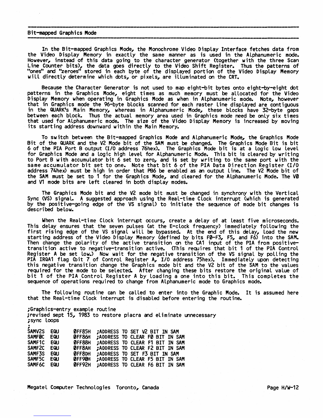
------------------------------------------------------------------------------
Bit-mapped
Graphics
Mode
In
the
Bit-mapped
Graphics Mode,
the
Monochrome Video
Display
Interface
fetches
data
from
the
Video
Display
Memory
in
exactly
the
same manner
as
is
used
in
the
Alphanumeric
mode.
However,
instead
of
this
data
going
to
the
character
generator
(together
with
the
three
Scan
Line
Counter
bits),
the
data
goes
directly
to
the
Video
Shift
Register.
Thus
the
patterns
of
"ones" and
"zeroes"
stored
in
each
byte
of
the
displayed
portion
of
the
Video
Display
Memory
will
directly
determine
which
oots,
or
pixels,
are
illuminated
on
the
CRT.
Because
the
Character
Generator
is
not used
to
map
eight-bit
bytes
onto
eight-by-eight
dot
patterns
in
the
Graphics
Mode,
eight
times
as
much
memory
must
be
allocated
for
the
Video
Display
Memory
when
operating
in
Graphics
Mode
as
when
in
Alphanumeric
mode.
Note, however
that
in
Graphics
mode
the
96-byte
blocks
scanned
for
each
raster
line
displayed
are
contiguous
in
the
QUARK's
Main Memory, whereas
in
Alphanumeric Mode,
these
blocks
have
32-byte
gaps
between each
block.
Thus
the
actual
memory
area
used
in
Graphics
mode
need
be
only
six
times
that
used
for
Alphanumeric mode.
The
size
of
the
Video
Display
Memory
is
increased
by moving
its
starting
address
oownward
within
the
Main
Memory.
To
switch
between
the
Bit-mapped
Graphics
Mode
and Alphanumeric Mode,
the
Graphics
Mode
Bit
of
the
QUARK
and
the
V2
Mode
bit
of
the
SAM
must
be
changed. The
Graphics
Mode
Bit
is
bit
6
of
the
PIA
Port
B
output
(1/0
address
76hex). The Graphi
cs
Mode
bit
is
at
a
logic
low
level
for
Graphics
Mode
and a
logic
high
level
for
Alphanumeric
Mode.
This
bit
is
cLeared by
writing
to
Port
B
with
accumulator
bit
6
set
to
zero,
and
is
set
by
writing
to
the
same
port
with
the
same
accumulator
bit
set
to
one.
Note
that
bit
6
of
the
PIA
Data
Direction
Register
(1/0
address
74hex> must be high
in
order
that
PB6
be enabLed
as
an
output
Line. The
V2
Mode
bit
of
the
SAM
must
be
set
to
1
for
the
Graphi
cs
Mode, and
cleared
for
the
Alphanumeric
Mode.
The
V0
and
V1
mode
bits
are
left
cleared
in
both
display
modes.
The
Graphics
Mode
bit
and
the
V2
mode
bit
must be changed
in
synchrony
with
the
Vertical
Sync (vS)
signal.
A
suggested
approach
using
the
Real-time
Clock
interrupt
(which
is
generated
by
the
positive-going
edge
of
the
VS
signaL>
to
initiate
the
sequence
of
mode
bit
changes
is
described
below.
When
the
Real-time
CLock
interrupt
occurs,
create
a deLay
of
at
least
five
microseconds.
This
delay
ensures
that
the
seven
pulses
(at
the
E-clock
frequency)
immediately
following
the
first
rising
edge
of
the
VS
signal
will
be
bypassed.
At
the
end
of
this
delay,
load
the
new
starting
address
of
the
Video
Display
Memory
(defined
by
bits
F0-F3, FS, and
F6)
into
the
SAM.
Then change
the
polarity
of
the
active
transition
on
the
CA1
input
of
the
PIA
from
positive-
transition
active
to
negative-transition
active.
<This
requires
that
bit
1
of
the
PIA
Control
Register
A be
set
low.)
Now
wait
for
the
negative
transition
of
the
VS
signal
by
poLling
the
PIA
IRQA1
flag
(bit
7
of
Control
Register
A,
1/0
address
75hex). ImmediateLy upon
detecting
this
negative
transition
change
the
Graphics
mode
bit
and
the
V2
bit
of
the
SAM
to
the
values
requi
red
for
the
mode
to
be
selected.
After
changing
these
bits
restore
the
original
value
of
bit
1
of
the
PIA
Control
Register
A
by
Loading
a one
into
this
bit.
This
completes
the
sequence
of
operations
required
to
change from Alphanumeric
mode
to
Graphics
mode.
The
following
routine
can
be
calLed
to
enter
into
the
Graphic
Mode.
It
is
assumed
here
that
the
Real-time
Clock
interrupt
is
disabled
before
entering
the
routine.
iGraphics-entry
exampLe
routine
irevised
sept
15,
1983
to
restore
piacra
and
eliminate
unnecessary
isync
loops
.
,
SAMV2S
EQU
SAMF0C
EQU
SAMF1C
EQU
SAMF2C
EQU
SAMF3S
EQU
SAMFSC
EQU
SAMF6C
EQU
0FF85H
iADDRESS
TO
SET
V2
BIT
IN
SAM
0FF86H
iADDRESS
TO
CLEAR
F0
BIT
IN
SAM
0FF88H
iADDRESS
TO
CLEAR
F1
BIT
IN
SAM
0FF8AH
iADDRESS
TO
CLEAR
F2
BIT
IN
SAM
0FF8DH
iADDRESS
TO
SET
F3
BIT
IN
SAM
0FF90H
iADDRESS
TO
CLEAR
F5
BIT
IN
SAM
0FF92H
iADDRESS
TO
CLEAR
F6
BIT
IN
SAM
Megatel Computer
Technologies
Toronto,
Canada Page
H/W-12
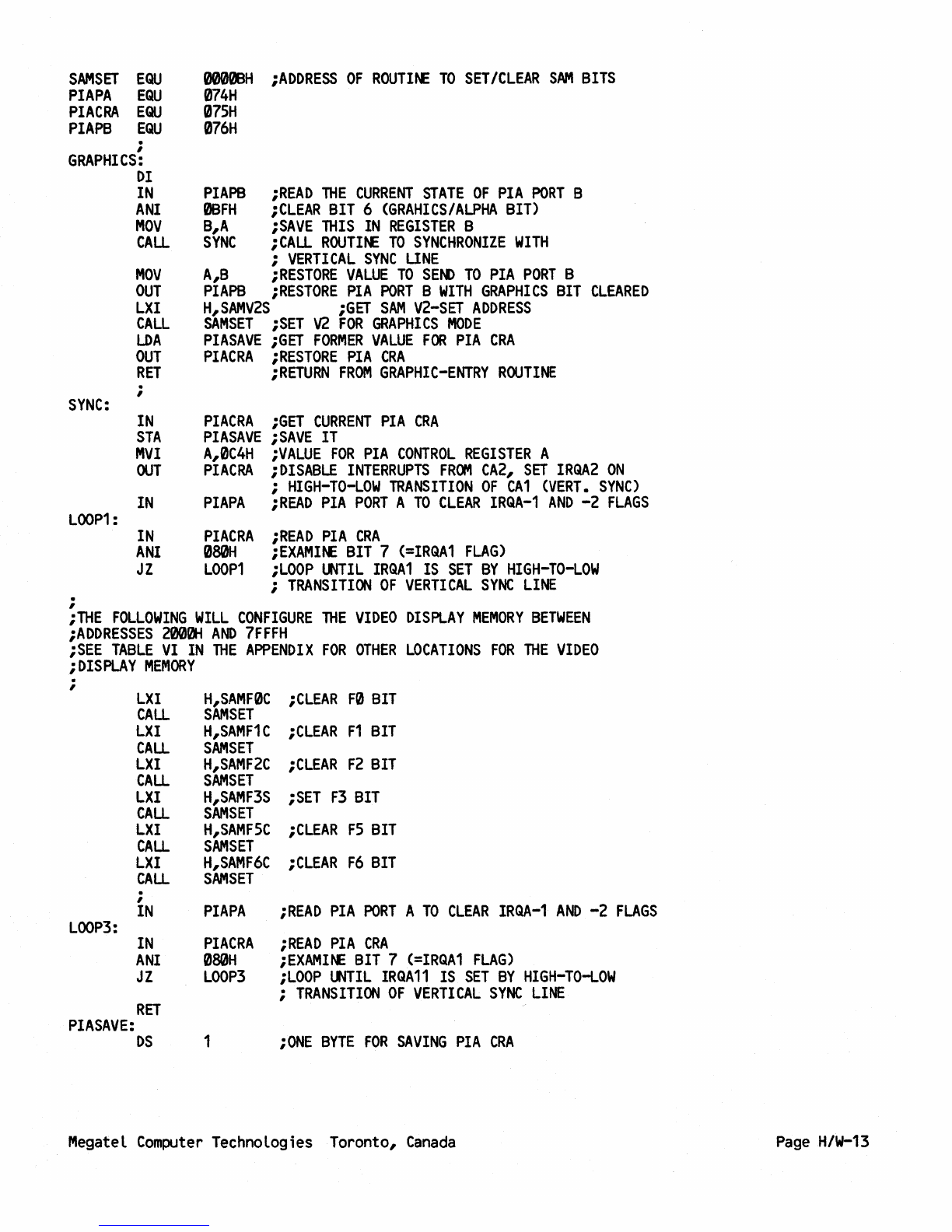
SAMSEl
EQU
PIAPA
EQU
PIACRA
EQU
PIAPB
EQU
0000BH
;ADDRESS
OF
ROUTINE
TO
SET/CLEAR
SAM
BITS
074H
075H
076H
i
GRAPHICS:
SYNC:
LooP1
:
.
,
DI
IN
ANI
MOV
CALL
MOV
OUT
LXI
CALL
lOA
OUT
RET
.
,
PIAPB
;READ
THE
CURRENT
STATE
OF
PIA
PORT
B
0BFH
;CLEAR
BIT
6
(GRAHICS/ALPHA
BIT)
B,A
iSAVE
THIS
IN
REGISTER
B
SYNC
iCALL
ROUTINE
TO
SYNCHRONIZE
WITH
i
VERTICAL
SYNC
LINE
A,B
iRESTORE
VALUE
TO
SEND
TO
PIA
PORT
B
PIAPB
;RESTORE
PIA
PORT
B
WITH
GRAPHICS
BIT
CLEARED
H,SAMV2S
;GEl
SAM
V2-SET
ADDRESS
SAMSET
;SET
V2
FOR
GRAPHICS
MODE
PIASAVE
iGET
FORMER
VALUE
FOR
PIA
CRA
PIACRA
;RESTORE
PIA
CRA
;RETURN
FROM
GRAPHIC-ENTRY
ROUTINE
IN
PIACRA
iGET
CURRENT
PIA
CRA
STA
PIASAVE
;SAVE
IT
MVI
A,0C4H
iVALUE
FOR
PIA
CONTROL
REGISTER
A
OUT
PIACRA
;DISABLE
INTERRUPTS
FROM
CA2,
SET
IRGA2
ON
i
HIGH-TO-LOW
TRANSITION
OF
CA1
(VERT.
SYNC)
IN
PIAPA
iREAD
PIA
PORT
A
TO
CLEAR
IRGA-1
AND
-2
FLAGS
IN
PIACRA
iREAD
PIA
CRA
ANI
080H
iEXAMINE
BIT
7
(=IRGA1
FLAG)
JZ
LOOP1
iLOOP
UNTIL
IRGA1
IS
SET
BY
HIGH-TO-LOW
i
TRANSITION
OF
VERTICAL
SYNC
LINE
iTHE
FOLLOWING
WILL
CONFIGURE
THE
VIDEO
DISPLAY
MEMORY
BETWEEN
iADDRESSES
2000H
AND
7FFFH
iSEE
TABLE
VI
IN
THE
APPENDIX
FOR
OTHER
LOCATIONS
FOR
THE
VIDEO
iDISPLAY
MEMORY
.
,
LXI
H,SAMF0C
;CLEAR
F0
BIT
CALL
SAMSET
LXI
H,SAMF1C
iCLEAR
F1
BIT
CALL
SAMSET
LXI
H,SAMF2C
;CLEAR
F2
BIT
CALL
SAMSET
LXI
H,SAMF3S
iSET
F3
BIT
CALL
SAMSET
LXI
H,SAMF5C
;CLEAR
F5
BIT
CALL
SAMSET
LXI
H,SAMF6C
iCLEAR
F6
BIT
CALL
SAMSET
.
,
IN
PIAPA
iREAD
PIA
PORT
A
TO
CLEAR
IRQA-1
AND
-2
FLAGS
LooP3:
IN
PIACRA
iREAD
PIA
CRA
ANI
080H
iEXAMlNE
BIT
7
(=IRQA1
FLAG)
JZ
LOOP3
iLOOP
UNTIL
IRQA11
IS
SET
BY
HIGH-TO-LOW
i
TRANSITION
OF
VERTICAL
SYNC
LINE
RET
PIASAVE:
DS
1
iONE
BYTE
FOR
SAVING
PIA
CRA
Megatel
Computer
Technologies Toronto,
Canada
Page
H/W-13

The
example
and
description
above
assumed
that the interrupts
were
disabled throughout the
procedure.
It
would
also
be
possible to re-enable interrupts
after
loading the
Video
Memory
starting
address
and
changing
the polarity of the
CA1
active transition.
The
next negative
transition
of the
VS
signal
would
generate
an
interrupt, immediately following
which
the
Graphics
mode
bit
and
the
V2
bit
would
be
changed,
just
as
in the non-interrupt procedure
above.
To
return
to
Alphnumeric
mode,
it
is necessary only to set the Graphics/Alphanumeric
mode
bit,
and
then clear the
V2
bit
in the
SAM,
and
set
up
the F-bits for the desired
Video
Display
Memory
location.
The
routine
below
wi
II
set up the
Alphanumeric
mode
with the
Video
Display
Memory
located between
F000
and
FFFF,
as is set up
by
the Bootstrap
PROM.
;alpha-entry
example
routine
SAMV2C
EQU
0FF84H
iADDRESS
TO
CLEAR
V2
BIT
IN
SAM
SAMF0C
EQU
0FF86H
;ADDRESS
TO
CLEAR
F0
BIT
IN
SAM
SAMF1C
EQU
0FF88H
;ADDRESS
TO
CLEAR
F1
BIT
IN
SAM
SAMF2S
EQU
0FF8BH
;ADDRESS
TO
SET
F2
BIT
IN
SAM
SAMF3S
EQU
0FF8DH
;ADDRESS
TO
SET
F3
BIT
IN
SAM
SAMFSS
EQU
0FF91H
;ADDRESS
TO
SET
FS
BIT
IN
SAM
SAMF6S
EQU
0FF93H
;ADDRESS
TO
SET
F6
BIT
IN
SAM
PIAPA
EQU
074H
PIACRA
EQU
07SH
PIAPB
EQU
076H
SAMSET
EQU
0000BH
ALPHA:
.
,
.
,
iTO
AVOID
GLITCHING
SCREEN,
THIS
POINT
SHOULD
SYNCHRONIZED
WITH
iVERTICAL
SYNC
SIGNAL
(SEE
GRAPHICS-ENTRY
EXAMPLE)
DI
;DISABLE
INTERRUPTS
IN
PIAPB
iREAD
CONTENTS
OF
PIA
PORT
B
OUTPUT
ORI
40H
;SET
BIT
6
FOR
ALPHANUMERIC
MODE
OUT
PIAPB
LXI
H,SAMV2C
CALL
SAMSET
LXI
H,SAMF0C
CALL
SAMSET
LXI
H,SAMF1C
CALL
SAMSET
LXI
H,SAMF2S
CALL
SAMSET
LXI
H,SAMF3S
CALL
SAMSET
LXI
H,SAMFSS
CALL
SAMSET
LXI
H,SAMF6S
CALL
SAMSET
EI
RET
This completes the routine to switch
from
graphics
mode
to alphanumeric
mode.
Loading
the
Programmable
Character Generator
On
the
QUARK
the patterns for the characters displayed
in
the
Alphanumeric
Mode
are
loaded
into
the
Character Generator under
software
control.
Once
loaded
the
contents
of
the
Character Generator
remain
unti l another character set
is
loaded
or untiC
power
to the
board
is
removed.
The
standard set
of
uti l
ity
routines included with the Distribution Software include
programs for loading the
Programmable
Character Generator
and
for designing character patterns
to
be loaded.
It
is
therefore
not
necessary to understand
how
the
Programmable
Character
Generator operates in order to
be
able to
make
use
of
this
feature.
Megatel
Computer
Technologies Toronto,
Canada
Page
H/W-14

-----------------,------
Peripheral Interfaces
-------,
The
Megatel
QUARK
provides a
number
of
parallel
and
serial
1/0
lines.
While
some
of these
lines are intended for
use
with specific peripherals,
such
as
parallel-
or
serial-interface
printers,
many
of these
1/0
lines
may
be
used
for
more
general purposes
if
the intended devices
are not being
used
in a
particular
application. Adiscussion of these
1/0
ports follows. In
addition, specialized peripheral subsystems,
such
as
the Floppy-disk Controller provide a high
level of
1/0
support. ------------------------
Parallel
Printer
Interface
-_.
_
..
---------------
The
QUARK
includes a port intended for the connection of
an
eight-bit
parallel-interface
printer.
This port consists of
an
eight-bit
latch for the output data, a
Data
Strobe output
line,
and
an
Acknowledge
input line. All of the input
and
output lines for
this
port are
TTL-
compatible.
Eight-bit
parallel
data is written to the port
by
an
output instruction
to
1/0
address
5Fhex.
The
data appearing
on
the output pins of the
QUARK
(see Table I for the pinout of the
connector) represent the true
state
of the data written to the port.
The
Data
Strobe line for the port is controlled
by
the
CA2
control line of the
VIA.
The
CA2
control line
must
be configured
as
an
output in the Peripheral Control Register
(PCR)
of
the
VIA,
by
setting
bits
2
and
3 of the
PCR.
The
CA2
output drives a
TTL
inverter, the output
of
which
is connected to the
Data
Strobe output pin (pin
C-13).
Thus
the logic
state
of the
actual
Data
Strobe output
is
the inverse of the
state
of the
CA2
line,
as determined
by
bit
1
of the
PCR.
This
TTL
inverter is capable of sinking
24mA.
The
Acknowledge
input for the Parallel Printer Port
is
directly
connected
to
the
CA1
input
line of the
VIA.
The
active
transition
of the
CA1
input of
this
line
wi
II
set
a flag in the
Interrupt
Flag
Register
(IFR)
of
the
VIA.
The
setting
of
this
flag
may
also
generate
an
interrupt
if
the appropriate
bit
in the Interrupt
Enable
Register
CIER)
of the
VIA
is
set.
This interrupt
can
be
used
to interrupt the
CPU
when
the
printer
is
ready
to
accept another
character,
depending
on
the operation of the printer.
Handshaking
using the
Data
Strobe
and
Acknowledge
lines
is
not
automatic, that
is
that the
routine
handl
ing
the
Parallel
Printer Interface
must
write the output latch, toggle the
Data
Strobe line
in
the
manner
required for the interface of the
printer,
and
then act accordingly
for the
printer's
response
on
the
Acknowledge
input.
If
it
is
not
desired
to
use
this
port with a
parallel
printer,
then the eight
Data
lines,
the
Acknowledge Input
line,
and
the
inverted
output
line
from
CA2
may
be used
for
other
purposes
such
as
might
be required for a
particular
application of the
QUARK.
--,------,
Parallel
Keyboard
Interface -------------
The
QUARK
provides
an
interface for
an
ASCII-encoded
parallel-output
keyboard. This
interface uses the Port A 1/0 lines
and
the
CA2
control line of the
PIA.
As
initial
ized
by
standard
CP/M
operating systems provided
on
the Distribution Diskettes, active-high
ASCII
data
present
on
the
PAD-7
lines of the
PIA
will
be
read
after
a negative-going stobe pulse
on
CA2.
Note
that the data present
on
the input lines is
not
actually latched into the Input
Data
register
when
the strobe occurs,
so
the
keyboard
data
must
remain
valid
between
the strobe
and
the read.
(This
is
not
usua
lly
a problem.)
If
it
is
not intended
to
use
an
encoded keyboard
for
a
particular
application
of
the
QUARK,
then
these
eight
1/0
lines
and
the
CA2
control
line
may
be
used
for
any
other
1/0
functions
which
might
be
required.
It
is
possible, for instance,
to
connect
an
un-encoded
Megatel
Computer
Technologies Toronto,
Canada
Page
H/W-15
Table of contents


