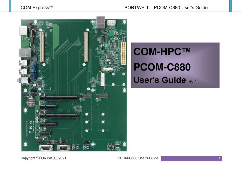
Memec Virtex-II V2MB1000 User manual

Virtex-II™ V2MB1000
Development Board
User’s Guide
Version 3.0
December 2002
PN# DS-MANUAL-V2MB1000

Memec Design Development Kit Owners Certificate
Thank you for purchasing your Memec Design development kit. As an owner of
this kit, you can register for access to the Reference Design Center. In the
Reference Design Center, you may download reference design examples for this
particular kit, along with source code, and application notes. As more reference
designs are added, you will be notified via e-mail. Visit the Reference Design
Center today at:
http://legacy.memec.com/solutions/reference/xilinx/
Your kit serial number is:
For technical assistance, contact your local Memec Design distributor office
(Memec, Insight or Impact) or send an e-mail to:

WARRANTY AND LIABILITY DISCLAIMER
Notwithstanding any additional, different or conflicting terms or conditions contained in the
purchaser’s ordering document or other document, to the maximum extent permitted by applicable
law, Memec, LLC and its subsidiaries (“Insight” and “Impact”) expressly disclaim all warranties,
conditions, or representations, express, implied, statutory or otherwise, regarding this product or
any other services provided by Memec in connection with this product, all of which are provided “as
is”, and this disclaimer shall apply to any implied warranties or conditions of merchantability,
satisfactory or merchantable quality and fitness for a particular purpose, or those arising from a
course of dealing or usage of trade.
Under no circumstances (to the maximum extent permitted by applicable law), shall Memec be
liable to the purchaser or to any third party, for a claim of any kind arising as a result of, or related
to the product, whether in contract, in tort (including negligence or strict liability), under any
warranty, or otherwise. This limitation of liability shall apply notwithstanding the fact that a claim
brought by the purchaser or any third party is for indirect, special or consequential damages
(including lost profits), even if Memec has been advised of the possibility of such damages, or for
warranties granted by the purchaser to any third party.
The purchaser acknowledges and agrees that the price for this product is based in part upon these
limitations, and further agrees that these limitations shall apply notwithstanding any failure of
essential purpose of any limited remedy.

December 2,2002 i
Table of Contents
1OVERVIEW....................................................................................................................1
2THE VIRTEX-II SYSTEM BOARD...................................................................................1
2.1 VIRTEX-II SYSTEM BOARD DESCRIPTION......................................................................2
2.2 VIRTEX-II DEVICE .....................................................................................................2
2.3 DDR MEMORY .........................................................................................................3
2.4 CLOCK GENERATION .................................................................................................4
2.5 RESET CIRCUIT........................................................................................................5
2.6 USER 7-SEGMENT DISPLAY........................................................................................5
2.6.1 7-Segment Display Signal Description..................................................................6
2.7 USER LED...............................................................................................................6
2.8 USER PUSH BUTTON SWITCHES (SW5, AND SW6) ........................................................6
2.8.1 User Push Button Switch Signal Assignments.......................................................6
2.9 USER DIP SWITCH (SW2) .........................................................................................6
2.9.1 User DIP Switch Interface ...................................................................................6
2.9.2 User DIP Switch Signal Assignments...................................................................7
2.10 RS232 PORT...........................................................................................................7
2.10.1 RS232 Interface..............................................................................................7
2.10.2 RS232 Signal Descriptions ..............................................................................8
2.11 JTAG PORT ............................................................................................................8
2.11.1 Standard JTAG Connector ..............................................................................8
2.11.2 Parallel Cable IV Port......................................................................................8
2.11.3 JTAG Chain ...................................................................................................9
2.11.4 JTAG Chain Jumper Settings ..........................................................................9
2.12 SELECTMAP/SLAVE SERIAL PORT...............................................................................9
2.12.1 Slave SelectMap...........................................................................................10
2.12.2 Master SelectMap.........................................................................................10
2.13 SLAVE SERIAL PORT ...............................................................................................11
2.14 BANK I/O VOLTAGE.................................................................................................11
2.14.1 Bank I/O Voltage Jumper Settings .................................................................11
2.15 VIRTEX-II POWER DOWN MODE................................................................................12
2.16 VIRTEX-II VBAT.....................................................................................................13
2.17 ISP PROM ...........................................................................................................13
2.18 LVDS PORT..........................................................................................................14

December 2,2002 ii
2.18.1 LVDS Interface.............................................................................................14
2.18.2 LVDS Port Signal Descriptions ......................................................................17
2.18.3 Packet Over SONET Level 4 (PL4) application...............................................19
2.19 PROGRAM SWITCH (SW2) .......................................................................................20
2.20 VOLTAGE REGULATORS...........................................................................................20
2.20.1 Voltage Regulators Jumper Settings ..............................................................21
2.21 VIRTEX-II CONFIGURATION MODE SELECT..................................................................22
2.22 P160 EXPANSION MODULE SIGNAL ASSIGNMENTS.......................................................23
3DESIGN DOWNLOAD..................................................................................................25
3.1 JTAG INTERFACE...................................................................................................25
3.1.1 Configuring the Virtex-II FPGA...........................................................................25
3.1.2 Programming the XC18V04 ISP PROM..............................................................25
3.2 SLAVE SERIAL INTERFACE........................................................................................26
3.3 MASTER SELECTMAP INTERFACE ..............................................................................26
3.4 SLAVE SELECTMAP INTERFACE.................................................................................26
REVISION HISTORY............................................................................................................27
APPENDIX A –VIRTEX-II SYSTEM BOARD SCHEMATICS..................................................28

December 2,2002 iii
Figures
FIGURE 1 –VIRTEX-II SYSTEM BOARD.........................................................................................1
FIGURE 2–VIRTEX-II SYSTEM BOARD BLOCK DIAGRAM.................................................................2
FIGURE 3–DDR INTERFACE......................................................................................................3
FIGURE 4–RESET CIRCUIT........................................................................................................5
FIGURE 5-7-SEGMENT LED DISPLAY INTERFACE.........................................................................5
FIGURE 6–USER DIP SWITCH INTERFACE...................................................................................7
FIGURE 7 –RS232 INTERFACE ..................................................................................................7
FIGURE 8–J2 JTAG CONNECTOR .............................................................................................8
FIGURE 9 –JP29 PARALLEL IV PORT..........................................................................................8
FIGURE 10–VIRTEX-II SYSTEM BOARD JTAG CHAIN....................................................................9
FIGURE 11–SELECTMAP/SLAVE SERIAL CONNECTOR.................................................................10
FIGURE 12–SLAVE SELECTMAP MODE CONFIGURATION .............................................................10
FIGURE 13–MASTER SELECTMAP MODE CONFIGURATION...........................................................11
FIGURE 14–SLAVE SERIAL MODE CONFIGURATION.....................................................................11
FIGURE 15–VIRTEX-II POWER DOWN MODE..............................................................................13
FIGURE 16–ISP PROM INTERFACE.........................................................................................14
FIGURE 17–LVDS TRANSMIT PORT.........................................................................................15
FIGURE 18–LVDS RECEIVE PORT ...........................................................................................16
FIGURE 19–LVDS TRANSMIT AND RECEIVE CONTROL PORTS ......................................................16
FIGURE 20–PACKET OVER SONET LEVEL 4 (PL4) INTERFACE ...................................................20
FIGURE 21–VIRTEX-II DEVELOPMENT BOARD VOLTAGE REGULATORS ..........................................21
FIGURE 22–DOWNLOAD SETUP...............................................................................................25

December 2,2002 iv
Tables
TABLE 1 -DDR MEMORY INTERFACE SIGNAL DESCRIPTIONS ..........................................................3
TABLE 2 –VIRTEX-II DEVELOPMENT BOARD MASTER CLOCKS.........................................................4
TABLE 3 -7-SEGMENT DISPLAY SIGNAL DESCRIPTIONS ..................................................................6
TABLE 4 -USER PUSH BUTTON SWITCH SIGNAL ASSIGNMENTS .......................................................6
TABLE 5 -USER DIP SWITCH SIGNAL ASSIGNMENTS......................................................................7
TABLE 6 -RS232 SIGNAL DESCRIPTIONS.....................................................................................8
TABLE 7 -JTAG CHAIN JUMPER SETTINGS ..................................................................................9
TABLE 8 -BANK I/O VOLTAGE JUMPER SETTINGS........................................................................12
TABLE 9 -LVDS TRANSMIT PORT SIGNAL DESCRIPTIONS.............................................................17
TABLE 10 -LVDS RECEIVE PORT SIGNAL DESCRIPTIONS.............................................................18
TABLE 11-LVDS TRANSMIT CONTROL PORT SIGNAL DESCRIPTIONS..............................................19
TABLE 12-LVDS RECEIVE CONTROL PORT SIGNAL DESCRIPTIONS ...............................................19
TABLE 13 -VOLTAGE REGULATORS JUMPER SETTINGS ................................................................21
TABLE 14 -VIRTEX-II CONFIGURATION MODE SELECT..................................................................22
TABLE 15 –JX1 USER I/O CONNECTOR....................................................................................23
TABLE 16 –JX2 USER I/O CONNECTOR....................................................................................24

December 2,2002 1
1Overview
The Virtex-II V2MB1000 Development Kit provides a complete solution for developing designs
and applications based on the Xilinx Virtex-II FPGA family. The kit bundles an expandable Virtex-
II based system board with a power supply, user guide and reference designs. Also available
from Memec Design, optional P160 expansion modules enable further application specific
prototyping and testing. Xilinx ISE software and a JTAG cable are available as kit options.
The Virtex-II system board utilizes the 1-million gate Xilinx Virtex-II device (XC2V1000-4FG456C)
in the 456 fine-pitch ball grid array package. The high gate density and large number of user I/Os
allows complete system solutions to be implemented in the advanced platform FPGA. The
system board includes a 16M x 16 DDR memory, two clock sources, RS-232 port, and additional
support circuits. An LVDS interface is provided with a 16-bit transmit and 16-bit receive port plus
clock, status, and control signals for each. The board also supports the Memec Design P160
expansion module standard, allowing application specific expansion modules to be easily added.
The Virtex-II FPGA family has the advanced features needed to fit demanding, high-performance
applications. The Virtex-II Development Kit provides an excellent platform to explore these
features so that you can quickly and effectively meet your time-to-market requirements.
2The Virtex-II System Board
The Memec Design Virtex-II System Board provides the FPGA, support circuits and the P160
expansion slot for application specific add-on cards. Figure 1 shows a picture of the board and its
features.
Figure 1–Virtex-II System Board

December 2,2002 2
2.1 Virtex-II System Board Description
A high-level block diagram of theVirtex-II development board is shown in Figure 2 followed by a brief
description of each sub-section.
3.3V
Regulator
2.5V
Regulator
User
7-Segment
Display (2)
RS232
Port
JTAG Port
ISP PROM
(XC18V04)
User
Switches
User
LEDs
SlaveSerial/
SelectMap
Clock Generator
(100 & 24Mhz)
Virtex-II FPGA
XC2V1000
(FG456)
Reset
Circuit
80-Pin Connector
80-Pin Connector
P160 Module
32MB
DDR SDRAM
16-bit
LVDS Interface
1.5V
Regulator
Voltage
Regulators
Figure 2–Virtex-II System Board Block Diagram
2.2 Virtex-II Device
The Virtex-II board utilizes the Xilinx Virtex-II XC2V1000-4FG456C. The Virtex-II family is a
platform FPGA developed for high performance, low to high-density designs utilizing IP cores and
customized modules. The Virtex-II family delivers complete solutions for telecommunication,
wireless, networking, video, and DSP applications. The performance and density of the Virtex-II
family along with its supported I/O standards such as LVDS, PCI, and DDR enables FPGA
designers to meet the design requirements of the next generation Networking and
telecommunication applications. The Xilinx Virtex-II FPGA along with its supporting I/O devices
on this development board, will assist FPGA designers to prototype high-performance memory
and I/O interfaces such as complete high-performance Packet Over SONET Level 4 (PL4) over a
16-bit LVDS bus, high speed DDR memory interface, and a variety of other I/O interfaces via the
on-board I/O module.

December 2,2002 3
2.3 DDR Memory
The Virtex-II development board provides 32MB of DDR memory on the system board. This
memory is implemented using the Micron MT46V16M16TG-75 16Mx16 DDR device. A high-level
block diagram of the DDR interface is shown below followed by a table describing the DDR
memory interface signals.
Virtex-II
FPGA 16M x 16 DDR
(MT46V16M16TG-75)
Addr[12:0]
Data[15:0]
BS[1:0]
LDM
UDM
LDQS
UDQS
CSn
RASn
CASn
WEn
CLK
CLKn
CLKE
OSC
100Mhz clk_in
clk_fb
reset
Figure 3–DDR Interface
Table 1-DDR Memory Interface Signal Descriptions
Signal Name Description FPGA Pin # DDR Pin #
A0 Address 0 B18 29
A1 Address 1 A18 30
A2 Address 2 B17 31
A3 Address 3 A17 32
A4 Address 4 N17 35
A5 Address 5 P18 36
A6 Address 6 P17 37
A7 Address 7 M18 38
A8 Address 8 M19 39
A9 Address 9 M20 40
A10 Address 10 A19 28
A11 Address 11 N18 41

December 2,2002 4
A12 Address 12 N20 42
DQ0 Data 0 Y21 2
DQ1 Data 1 Y22 4
DQ2 Data 2 W21 5
DQ3 Data 3 V21 7
DQ4 Data 4 V22 8
DQ5 Data 5 U21 10
DQ6 Data 6 U22 11
DQ7 Data 7 T21 13
DQ8 Data 8 R20 54
DQ9 Data 9 R19 56
DQ10 Data 10 T20 57
DQ11 Data 11 T19 59
DQ12 Data 12 U19 60
DQ13 Data 13 V20 62
DQ14 Data 14 V19 63
DQ15 Data 15 W20 65
BS0 Bank Select 0 M21 26
BS1 Bank Select 1 B19 27
LDM Low Write Mask R21 20
UDM High Write Mask T22 47
LDQS Low Write/Read Data Strobe P20 16
UDQS High Write/Read Data Strobe P19 51
CSn Chip Select N22 24
RASn Row Address Strobe N21 23
CASn Column Address Strobe P21 22
WEn Write Enable R22 21
CLK Clock D12 45
CLKn Clock E12 46
CKE Clock Enable N19 44
2.4 Clock Generation
The Virtex-II system board provides two on-board oscillators running at 100Mhz (CLK.CAN2) and
24Mhz (CLK.CAN1). The 100Mhz oscillator is enabled when the JP24 jumper is open and
disabled when JP24 is closed. JP23 controls the 24MHz oscillator, enabling it when open and
disabling it when closed. A third user clock socket is provided for addition of a user specified
oscillator device. The following table provides a brief description of these clock signals.
Table 2–Virtex-II Development Board Master Clocks
Signal Name Virtex-II Pin # Direction Description
CLK.CAN2 B11 Input On-board 100 MHz Oscillator
CLK.CAN1 A11 Input On-board 24 MHz Oscillator
CLK.CAN3 F12 Input User clock socket (2.5V supply)

December 2,2002 5
2.5 Reset Circuit
The Virtex-II system board uses the TI TPS3125 voltage supervisory device to monitor the Virtex-
II FPGA core voltage (1.5V). This circuit asserts a reset signal (FPGA_RESETn) to the Virtex-II
device when the 1.5V core voltage falls below its minimum specifications (1.425V). The reset
signal to the FPGA is a fixed 100ms active low pulse. In addition to monitoring the core voltage,
this circuit can be used to generate a reset pulse by activating the Master Reset (MRn) signal to
the TPS3125 device via the on-board push-button switch (SW3). The following figure shows the
reset circuit on the Virtex-II development board.
SW3
RESETn
MRn
VDD
TPS3125
FPGA_RESETn
1.5V
B6
FPGA
Figure 4–Reset Circuit
2.6 User 7-Segment Display
The Virtex-II system board utilizes two common-cathode 7-segment LED displays that can be
used during the test and debugging phase of a design. The user can turn a given segment on by
driving the associated signal high. The following figure shows the user 7-segment display
interface to the Virtex-II FPGA.
A1
B1
C1
D1
E1
F1 G1
A2
B2
C2
D2
E2
F2 G2
DISPLAY.1F
DISPLAY.1G
DISPLAY.1E
DISPLAY.1D
DISPLAY.1C
DISPLAY.1B
DISPLAY.1A
DISPLAY.2F
DISPLAY.2G
DISPLAY.2E
DISPLAY.2D
DISPLAY.2C
DISPLAY.2B
DISPLAY.2A
Figure 5-7-Segment LED Display Interface

December 2,2002 6
2.6.1 7-Segment Display Signal Description
The following table shows the 7-Segment LED display pin descriptions.
Table 3-7-Segment Display Signal Descriptions
Signal Name Virtex-II Pin # Description
DISPLAY.1A D9 7-Segment LED Display1, Segment A
DISPLAY.1B C9 7-Segment LED Display1, Segment B
DISPLAY.1C F11 7-Segment LED Display1, Segment C
DISPLAY.1D F9 7-Segment LED Display1, Segment D
DISPLAY.1E F10 7-Segment LED Display1, Segment E
DISPLAY.1F D10 7-Segment LED Display1, Segment F
DISPLAY.1G C10 7-Segment LED Display1, Segment G
DISPLAY.2A B9 7-Segment LED Display2, Segment A
DISPLAY.2B A8 7-Segment LED Display2, Segment B
DISPLAY.2C B8 7-Segment LED Display2, Segment C
DISPLAY.2D E7 7-Segment LED Display2, Segment D
DISPLAY.2E E8 7-Segment LED Display2, Segment E
DISPLAY.2F E10 7-Segment LED Display2, Segment F
DISPLAY.2G E9 7-Segment LED Display2, Segment G
2.7 User LED
The Virtex-II system board provides a single user LED. Pin A9 of the Virtex-II FPGA is used to
drive this active high signal.
2.8 User Push Button Switches (SW5, and SW6)
The Virtex-II system board provides two user push button switch inputs to the Virtex-II FPGA.
Each push button switch can be used to generate an active low signal.
2.8.1 User Push Button Switch Signal Assignments
The following table shows the pin assignments for the user push button switches.
Table 4-User Push Button Switch Signal Assignments
Signal Name Virtex-II Pin # Description
FPGA.PUSH1 D7 User Push Button Switch Input 1 (SW5)
FPGA.PUSH2 A6 User Push Button Switch Input 2 (SW6)
2.9 User DIP Switch (SW2)
The Virtex-II system board provides 8 user switch inputs. These switches can be statically set to
a low or high logic level.
2.9.1 User DIP Switch Interface
The following figure shows the user DIP switch interface to the Virtex-II FPGA.

December 2,2002 7
5
4
3
2
1
6
7
8
12
13
14
15
16
11
10
9
SW4
Switch
DIP8
DIP7
DIP6
DIP5
DIP4
DIP3
DIP2
DIP1
Figure 6–User DIP Switch Interface
2.9.2 User DIP Switch Signal Assignments
The following table shows the user switch pin assignments.
Table 5-User DIP Switch Signal Assignments
Signal Name Virtex-II Pin # Description
DIP8 C6 User Switch Input 8
DIP7 D6 User Switch Input 7
DIP6 A5 User Switch Input 6
DIP5 B5 User Switch Input 5
DIP4 C5 User Switch Input 4
DIP3 C4 User Switch Input 3
DIP2 A4 User Switch Input 2
DIP1 B4 User Switch Input 1
2.10 RS232 Port
The Virtex-II system board provides an RS232 port that can be driven by the Virtex-II FPGA. A
subset of the RS232 signals is used on the Virtex-II development board to implement this simple
interface (RD and TD signals).
2.10.1 RS232 Interface
The Virtex-II system board provides a DB-9 connection for a simple RS232 port. The board
utilizes the TI MAX3221 RS232 driver for driving the RD and TD signals. The user provides the
RS232 UART code, which resides in the Virtex-II FPGA.
RS232
Drivers
MAX3221
RXD
TXD
RD
TD
2
3
JDR1
Connector
Rout
Din
Rin
Dout
Figure 7–RS232 Interface

December 2,2002 8
2.10.2 RS232 Signal Descriptions
The following table shows the RS232 signals and their pin assignments to the Virtex-II FPGA.
Table 6-RS232 Signal Descriptions
Signal Name Virtex-II Pin # Description
RXD A7 Received Data, RD to DB9
TXD B7 Transmit Data, TD from DB9
2.11 JTAG Port
The Virtex-II development board provides a JTAG connector that can be used to program the on-
board ISP PROM and configure the Virtex-II FPGA. Two connector options are provided, J2 is a
1 x 7 header used to connect standard JTAG cable fly leads, and JP29 is used for connection of
the Xilinx Parallel IV JTAG cable.
2.11.1 Standard JTAG Connector
The following figure shows the pin assignments for the J2 JTAG connector on the Virtex-II
development board.
1
2
4
6
7
3
5
J2
JTAG
Connector
3.3V
GND
TCK
TDO
TDI
TMS
Figure 8–J2 JTAG Connector
2.11.2 Parallel Cable IV Port
The following figure shows the pin assignments for the Parallel Cable IV connector. The Parallel
Cable IV can also be used to configure the FPGA via Slave Serial configuration mode.
TCK/CCLK
TDO/DONE
TDI/DIN
TMS/PROG
JP20
Parallel
Cable IV
1 2
4
6
7
3
58
9 10
12
14
11
13
2.5V
Figure 9–JP29 Parallel IV Port

December 2,2002 9
2.11.3 JTAG Chain
The following figure shows the JTAG chain on the Virtex-II development board. Jumper JP22
provides the ability to remove the ISP PROM from the JTAG chain for direct connection to the
FPGA.
XC18V04
ISP
PROM
Virtex-II
FPGA
TDI TDO
TDI
TDI
TDO
TDO
TMS
TCK
TMS
TCK
TMS
TCK
JP221 2 3 4
Figure 10 –Virtex-II System Board JTAG Chain
2.11.4 JTAG Chain Jumper Settings
The following table shows the JTAG chain jumper setting on the Virtex-II development board.
Table 7-JTAG Chain Jumper Settings
Jumper Setting Description
1-2 Closed Disable PROMJP28 2-3 Closed Enable PROM (normal setting)
1-2, 3-4PROM in chain (normal setting)JP22 2-3Remove PROM from chain (FPGA only)
2.12 SelectMap/Slave Serial Port
In addition to the JTAG mode, the Virtex-II FPGA on the development board can be configured
using the Slave Serial or the SelectMap mode of configuration. The following figure shows the
connector pin assignments for the Slave Serial/SelectMap port.

December 2,2002 10
CCLK
DONE
CSn
INITn
J3
SelectMap/Slave Serial
Connector
1 2
4
6
7
9
3
5
8
11
13
15
10
12
14
16
PROGRAMn
RD/Wn
DOUT/BUSY
D0
D1
D2
D3
D4
D5
D6
D7
Figure 11 –SelectMap/Slave Serial Connector
2.12.1 Slave SelectMap
In the Slave SelectMAP configuration mode, a byte of configuration data is loaded into the Virtex-
II FPGA during each CCLK clock cycle. In this mode, an external source drives the CCLK clock
and the data bus containing the configuration data. The following figure shows the Slave
SelectMap configuration mode interface to the Virtex-II FPGA.
Virtex-II
FPGA
CCLK
DONE
CSn
INITn
PROGRAMn
RD/Wn
DOUT/BUSY
D[0:7] D[0:7]
DONE
CCLK
INIT_B
PROG_B
RDWR_B
BUSY
CS_B
Figure 12 –Slave SelectMap Mode Configuration
2.12.2 Master SelectMap
In the Master SelectMAP configuration mode, a byte of configuration data is loaded into the
Virtex-II FPGA during each CCLK clock cycle. In this mode, the Virtex-II FPGA drives the CCLK
clock while receiving configuration data from the PROM. The following figure shows the Master
SelectMap configuration mode interface to the Virtex-II FPGA. The JP27 jumper must be installed
when configuring the Virtex-II FPGA in the Master SelectMap mode.

December 2,2002 11
Virtex-II
FPGA
CCLK
DONE
CS_B
INIT_B
PROG_B
RDWR_B
D[0:7]
XC18V04 CF
CE
RESET/OE
CCLK
D[0:7]
JP27
Jumper
Figure 13 –Master SelectMap Mode Configuration
2.13 Slave Serial Port
In the Slave Serial configuration mode, a bit of configuration data is loaded into the FPGA during
each CCLK clock cycle. In this mode, an external source places the most significant bit of each
byte on the DIN pin first and then drives the CCLK clock to store data into the FPGA. The
following figure shows the Slave Serial configuration mode interface to the Virtex-II FPGA.
Virtex-II
FPGA
CCLK
DONE
INITn
PROGRAMn
D0 DIN
DONE
CCLK
INIT_B
PROG_B
Figure 14 –Slave Serial Mode Configuration
2.14 Bank I/O Voltage
The Virtex-II development board allows the Virtex-II I/O pins to be configured for 2.5V or 3.3V
operation. All Virtex-II user I/O pins are grouped in 8 different banks. Each bank of I/O pins on
the board can be configured to operate in the 2.5V or the 3.3V mode.
2.14.1 Bank I/O Voltage Jumper Settings
The following table shows the jumper settings for the Virtex-II bank I/O voltage (VCCO) selection.
Each bank can be set to 2.5V or 3.3V.

December 2,2002 12
Table 8-Bank I/O Voltage Jumper Settings
Bank # Virtex-II VCCO
Pin # Jumper
JP18
1-22-3
I/O Voltage
Closed Open 3.3V
0
Open Closed 2.5V
1FIXED 2.5V
JP26
1-22-3
Closed Open 3.3V
2
Open Closed 2.5V
3FIXED 2.5V
J19
1-22-3
Closed Open 3.3V
4
Open Closed 2.5V
J20
1-22-3
Closed Open 3.3V
5
Open Closed 2.5V
J21
1-22-3
Closed Open 3.3V
6
Open Closed 2.5V
J21
1-22-3
Closed Open 3.3V
7
Open Closed 2.5V
2.15 Virtex-II Power Down Mode
The Virtex-II FPGA family utilizes a dedicated pin called PWRDWN_B that can be used to place
the Virtex-II FPGA into a low-power and inactive state. In the normal operating mode, the
PWRDWN_B pin would be pulled up. Forcing the PWRDWN_B pin to logic 0 would place the
Virtex-II FPGA in power-down mode. The following figure shows the Virtex-II Power Down on the
Virtex-II development board.

December 2,2002 13
3.3V
Virtex-II FPGA
PWRDWN_B
JP16
Jumper
Figure 15 –Virtex-II Power Down Mode
As shown in the above figure, the Virtex-II FPGA can be placed in the power-down mode on the
Virtex-II system board by closing the JP16 jumper (permanently placing it in the power-down
mode until the jumper is removed), or by forcing the pin 2 of the JP16 to a logic 0 under user
control. The Virtex-II board users can use this pin to place the Virtex-II FPGA in the power-down
mode momentarily.
The Virtex-II FPGA provides Power-Down status information via the DONE pin if the
PWRDWN_STAT option is selected using BitGen. The DONE pin is asserted upon entry to the
power-down mode. After a successful wake-up, the DONE status pin is de-asserted (The wake-
up sequence is the reverse of the power-down sequence). While in power-down mode, the only
active pins are the PWRDWN_B and DONE. All inputs are off and all outputs are 3-stated.
While in the Power-Down state, the Power On Reset (POR) circuit is still active, but it does not
reset the device if VCCINT, VCCO, or VCCAUX falls below its minimum value. The POR circuit
waits until the PWRDWN_B pin is released before resetting the device. Also, the PROG_B pin is
not sampled while the device is in the Power-Down state. The PROG_B pin becomes active
when the PWRDWN_B pin is released. Therefore, the device cannot be reset while in the Power-
Down state.
2.16 Virtex-II VBAT
The Virtex-II VBAT input pin (pin A21) is connected to the 3.3V supply on the Virtex-II
development board through the JP15 jumper.
2.17 ISP PROM
The Virtex-II system board utilizes the Xilinx XC18V04 ISP PROM, allowing FPGA designers to
quickly download revisions of a design and verify the design changes in order to meet the final
system-level design requirements. The XC18V04 ISP PROM uses two interfaces to accomplish
the configuration of the Virtex-II FPGA.
Table of contents
Popular Computer Hardware manuals by other brands

Radica Games
Radica Games DAVID-II 716 Operating and maintenance instruction manual
Leica BIOSYSTEMS
Leica BIOSYSTEMS HistoCore PEGASUS Instructions for use
Texas Instruments
Texas Instruments DAC8803/14 EVM user guide

Meinberg
Meinberg GPS167PC operating instructions
SMC Networks
SMC Networks EX510-GPR1 Series Operation manual

Agility Technologies
Agility Technologies ReadyTechGo user guide
