HAL1820, HAL24xy, HAL28xy, HAL36xy, HAL38xy APPLICATION NOTE
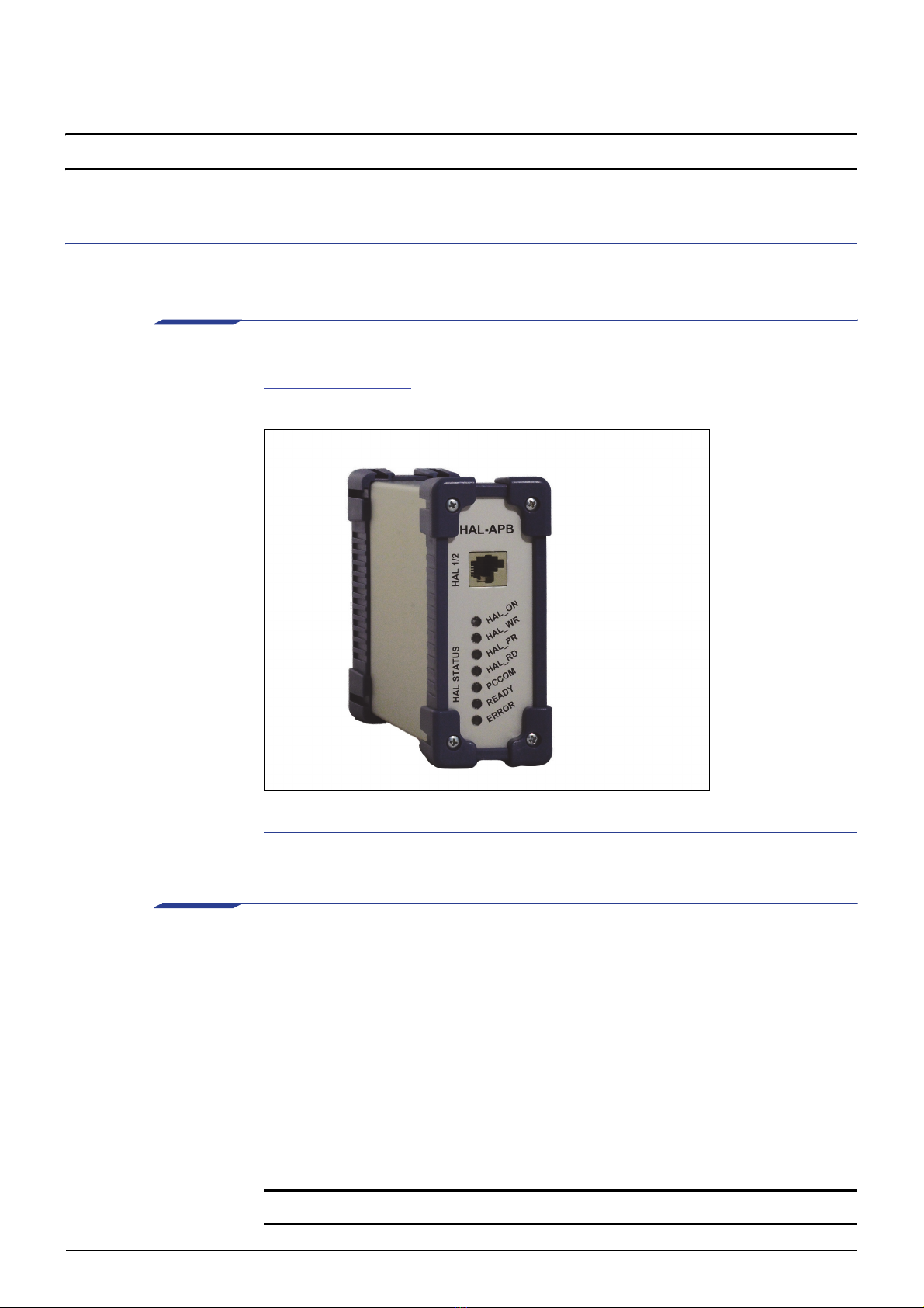
Application Board HAL-APB V1.x
2Oct. 8, 2012; APN000055_003EN Micronas
Copyright, Warranty,
and Limitation of
Liability
The information and data contained in this document are believed to be accurate and
reliable. The software and proprietary information contained therein may be protected
by copyright, patent, trademark and/or other intellectual property rights of Micronas. All
rights not expressly granted remain reserved by Micronas.
Micronas assumes no liability for errors and gives no warranty representation or guar-
antee regarding the suitability of its products for any particular purpose due to these
specifications.
By this publication, Micronas does not assume responsibility for patent infringements or
other rights of third parties which may result from its use. Commercial conditions, prod-
uct availability and delivery are exclusively subject to the respective order confirmation.
Any information and data which may be provided in the document can and do vary in
different applications, and actual performance may vary over time.
All operating parameters must be validated for each customer application by custom-
ers’ technical experts. Any new issue of this document invalidates previous issues.
Micronas reserves the right to review this document and to make changes to the docu-
ment’s content at any time without obligation to notify any person or entity of such revi-
sion or changes. For further advice please contact us directly.
Do not use our products in life-supporting systems, military, aviation, or aerospace
applications! Unless explicitly agreed to otherwise in writing between the parties, Micro-
nas’ products are not designed, intended or authorized for use as components in sys-
tems intended for surgical implants into the body, or other applications intended to sup-
port or sustain life, or for any other application in which the failure of the product could
create a situation where personal injury or death could occur.
No part of this publication may be reproduced, photocopied, stored on a retrieval sys-
tem or transmitted without the express written consent of Micronas.
Micronas Trademarks HAL, varioHAL, 1D HAL, 2D HAL, 3D HAL
Third-Party Trademarks All other brand and product names or company names may be trademarks of their
respective companies.
License Note HAL36xy and HAL38xy use licenses of Fraunhofer Institute for Integrated Circuits IIS.