Mpression Helio Board User manual

2015/11/16 © Mpression by Macnica Group
http://www.m-pression.com
Reference Manual
Mpression Helio Board
Revision 1.3
2015/11/16

Mpression Helio Board
2Reference Manual - Mpression Helio Board
© Mpression by Macnica Group
© Mpression –Solutions by Macnica Group
Disclaimer
The information in this document (hereinafter called “Information”) is subject to change without notice.
Macnica Inc. (hereinafter called “Manufacturer”) makes no warranty of any kind regarding this document, or of
any liability arising out of the application or use of information in this document, and assumes no responsibility
for any errors that may appear in this document.
This document is distributed without any charge and reselling or copying without written authorization by
Manufacturer is restricted.
IN NO EVENT WILL MANUFACTURER BE LIABLE FOR ANY CONSEQUENTIAL, INDIRECT,
EXEMPLARY, SPECIAL, OR INCIDENTAL DAMAGES, INCLUDING ANY LOST DATA AND LOST
PROFITS, ARISING FROM OR RELATING TO YOUR USE OF THE INFORMATION, EVEN IF YOU HAVE
BEEN ADVISED OF THE POSSIBILITY OF SUCH DAMAGES. THE TOTAL CUMULATIVE LIABILITY OF
MANUFACTURER IN CONNECTION WITH YOUR USE OF THE INFORMATION IN THIS DOCUMENT,
WHETHER IN CONTRACT OR TORT OR OTHERWISE, WILL IN NO EVENT EXCEED THE AMOUNT OF
FEES PAID BY YOU TO MANUFACTURER HEREUNDER FOR USE OF THE INFORMATION. YOU
ACKNOWLEDGE THAT THE FEES, IF ANY, REFLECT THE ALLOCATION OF RISK SET FORTH IN THIS
AGREEMENT AND THAT MANUFACTURER WOULD NOT MAKE AVAILABLE THE DESIGN TO YOU
WITHOUT THESE LIMITATIONS OF LIABILITY.
The Design is not designed or intended for use in the development of on-line control equipment in hazardous
environments requiring failsafe controls, such as in the operation of nuclear facilities, aircraft navigation or
communications systems, air traffic control, life support, or weapons systems (“High-Risk Applications”).
Manufacturer specifically disclaims any express or implied warranties of fitness for such High-Risk
Applications. You represent that use of the Design in such High-Risk Applications is fully at your risk.

Mpression Helio Board
Reference Manual - Mpression Helio Board 3
© Mpression by Macnica Group
Index
1. For Ensuring Safe Use __________________________________________________________ 5
1.1 Legend ....................................................................................................................................... 5
1.2 Cautions ..................................................................................................................................... 5
1.3 Manufacturer Information......................................................................................................... 7
2. Unboxing ____________________________________________________________________ 8
3. The Helio Board Hardware Descriptions ___________________________________________ 9
3.1 Overview.................................................................................................................................... 9
3.2 Key Components ........................................................................................................................ 9
3.3 Block Diagram .......................................................................................................................... 10
4. The Helio board Components___________________________________________________ 11
4.1 Board Overview ....................................................................................................................... 11
4.2 Featured Device: Cyclone V SoC .............................................................................................. 14
4.2.1 I/O Resources ............................................................................................................................14
4.3 JTAG Configuration................................................................................................................... 15
4.3.1 HPS debugging and FPGA Programming over On-board USB-Blaster II ....................................15
4.3.2 HPS debugging over Mictor connector for In-Circuit Emulator.................................................16
4.3.3 FPGA Programming over External USB-Blaster .........................................................................16
4.4 Status Elements ....................................................................................................................... 18
4.5 Setup Elements ........................................................................................................................ 19
4.5.1 JTAG settings DIP switch ...........................................................................................................19
4.5.2 HPS operation mode settings Jumper .......................................................................................20
4.5.3 HPS reset push button...............................................................................................................20
4.5.4 Program configuration push button..........................................................................................21
4.5.5 MSEL pins Settings ....................................................................................................................22
4.6 Clock Circuitry .......................................................................................................................... 23
4.6.1 On board Oscillators..................................................................................................................23
4.6.2 Off-board inputs / outputs ........................................................................................................24
4.7 General User Input / Output.................................................................................................... 25
4.7.1 User-Defined push button.........................................................................................................25
4.7.2 User-Defined DIP Switch ...........................................................................................................25
4.7.3 User-Defined LEDs.....................................................................................................................26
4.7.4 Character LCD............................................................................................................................26
4.7.5 Debug Header ...........................................................................................................................27
4.8 Components and Interfaces..................................................................................................... 28
4.8.1 10 / 100 / 1000 Ethernet...........................................................................................................28
4.8.2 HSMC.........................................................................................................................................29
4.8.3 USB2.0 OTG ...............................................................................................................................33

Mpression Helio Board
4Reference Manual - Mpression Helio Board
© Mpression by Macnica Group
4.8.4 UART..........................................................................................................................................33
4.8.5 SD ..............................................................................................................................................34
4.8.6 I2C .............................................................................................................................................34
4.9 Memory ................................................................................................................................... 36
4.9.1 DDR3-SDRAM ............................................................................................................................36
4.9.2 QSPI Flash ROM.........................................................................................................................39
4.9.3 EEPROM ....................................................................................................................................39
4.10Power Supply ........................................................................................................................... 40
4.10.1 Power Distribution System........................................................................................................40
5. Document Revision History ____________________________________________________ 42

Mpression Helio Board
Reference Manual - Mpression Helio Board 5
© Mpression by Macnica Group
1. For Ensuring Safe Use
Be sure to follow the instructions given in this Manual which are intended to prevent harm to the
user and others as well as material damage.
1.1 Legend
Danger
Indicates an imminent hazardous situation which if not avoided will result in
death or serious injury.
Warning
Indicates a potentially hazardous situation which if not avoided could result in
death or serious injury.
Caution
Indicates a potentially hazardous situation which if not avoided may result in
minor or moderate injury or in property damage.
1.2 Cautions
Danger
Make sure to use the AC adapter (included in package) that is specified in this
Manual.
Using an AC adapter not meeting the specifications described in this Manual
will cause the kit to emit heat, explode, or ignite.
Warning
Do not apply strong impacts or blows to the kit.
Doing so may cause the kit to emit heat, explode, or ignite, or the equipment in
the kit to fail or malfunction. This may also cause fire.
Do not put the main unit or the AC adapter in cooking appliances such as
microwave ovens, or high-pressure containers.
Doing so might cause the main unit or AC adapter to emit heat, explode, ignite,
or emit smoke, or its parts to break or warp.
Do not wrap the main unit that is in use with cloth or other materials that are
likely to allow heat to build up inside the wrapping.
This will cause heat to build up inside the wrapping which may cause the main
unit to ignite or malfunction.
When disposing of the main unit, do not dispose of it along with general
household waste.
Throwing the main unit into fire may cause it to explode. Dispose of the
main unit following the laws, regulations, and ordinances governing
waste disposal.
Do not use the kit in places subject to extremely high or low temperatures or
severe temperature changes.
Doing so may cause the kit to fail or to malfunction.
Always be sure to use the kit in a temperatures ranging from 5°C to 35°C and a
humidity range of 0% to 85%.
Mpression Helio Board
6Reference Manual - Mpression Helio Board
© Mpression by Macnica Group
Warning
(Continued from
previous page)
Do not pull the power supply cable with excessive force or place heavy items on
it.
Do not damage, break, bundle, or tamper with the power supply cable.
Damaged parts of the power supply cable might cause a short circuit resulting
in fire or accidents involving electrical shock.
Do not unplug the power plug with wet or moist hands.
This might cause injuries or equipment malfunctions or failures due to
electrical shock.
Plug the power plug securely into the outlet.
If the power plug is not securely plugged into the outlet, it may cause accidents
involving electrical shock or fire due to heat emitted.
Do not connect many electrical cords to a single socket or connect an AC adapter
to an outlet that is not rated for the specified voltage.
Failing to do so may cause the equipment to malfunction or fail, or lead to
accidents involving electrical shock or fire due to heat emitted.
Periodically remove any dust accumulated on the power plug and around the
outlet (socket).
Do not use a power plug with dust accumulated on it because doing so will lead
to insulation failure due to moisture which may lead to fire.
Remove any dust on the power plug and around the outlet with dried cloth.
Do not place any containers such as cups or vases filled with water or other
liquid on this Board.
If this Board is exposed to water or other liquids it may cause the Board to
malfunction or lead to accidents involving electrical shock. If you spilled water
or other liquid on this Board, immediately stop using the Board, turn off the
power, and unplug the power plug. If you have any requests for repairs or
technical consultation, please contact the Manufacturer.
Caution
Do not place the kit on unstable places such as shaky stands or tilted locations.
Doing so may cause injuries or cause this Board to malfunction if the Board
should fall.
Do not attempt to use or leave the kit in places subject to strong direct sunlight
or other places subject to high temperatures such as in cars in hot weather.
Doing so might cause the kit to emit heat, break, ignite, run out of control,
warp, or malfunction.
Also, some parts of the equipment might emit heat causing burn injuries.
Unplug the power supply cable when carrying out maintenance of devices in
which the main unit is embedded.
Failure to do so may lead to accidents involving electrical shock.
Do not place this Board in locations where excessive force is applied to the
Board.
Failure to do so may cause the PC board to warp, leading to breakage of the PC
board, missing parts or malfunctioning parts.
When using the kit together with expansion boards or other peripheral devices,
be sure to carefully read each of their manuals and to use them correctly.
Manufacturer does not guarantee the operation of specific expansion boards or
peripheral devices when used in conjunction with this Board unless they are
specifically mentioned in this Manual or their successful operation with this
Caution
(Continued from
previous page)

Mpression Helio Board
Reference Manual - Mpression Helio Board 7
© Mpression by Macnica Group
Board has been confirmed in separate documents.
Be sure to turn off the power switch when moving this Board to connect to other
devices.
Failure to do so may cause this Board to fail or lead to accidents involving
electrical shock.
Do not clean this Board by using a rag containing chemicals such as benzine or
thinner.
Failure to do so will likely to cause this Board to deteriorate. When using a
chemical cloth be sure to comply with any directions or warnings.
Do not immediately turn on the power if you find that water or moisture had
condensed onto the main unit after removing the board from the package.
Condensation might occur on this Board when taking it out of the box, if the
board is cool yet the room temperature is warm.
Do not apply power to the Board while water or moisture has condensed on it
because the moisture may cause the Board to break or may shorten the service
life of the parts.
When you first take this Board out of the box be sure to leave it at room
temperature for a while before using it. If condensation or moisture has
occurred on this Board, first wait for the moisture to fully evaporate before
installing or connecting the Board to other devices.
Do not disassemble, dismantle, modify, alter, or recycle parts unless they are
clearly described as customizable in this Manual.
Although this kit is customizable, if parts not specified in this Manual as
customizable are modified in any way, then the overall product operation
cannot be guaranteed.
Please consult with Manufacturer beforehand if you wish to customize or modify
any parts that are not described in this Manual as customizable.
1.3 Manufacturer Information
The Manufacturer of this product is:
Macnica, Inc. | Strategic Technology Group
Mpression
1-6-3 Shin-Yokohama, Kouhoku-ku, Yokohama, 222-8561 Japan
http://www.m-pression.com
Please contact through web site.
Mpression Helio Board
8Reference Manual - Mpression Helio Board
© Mpression by Macnica Group
2. Unboxing
Package Components
This product consists of the following board and peripherals. Please make sure all components
listed below are included.
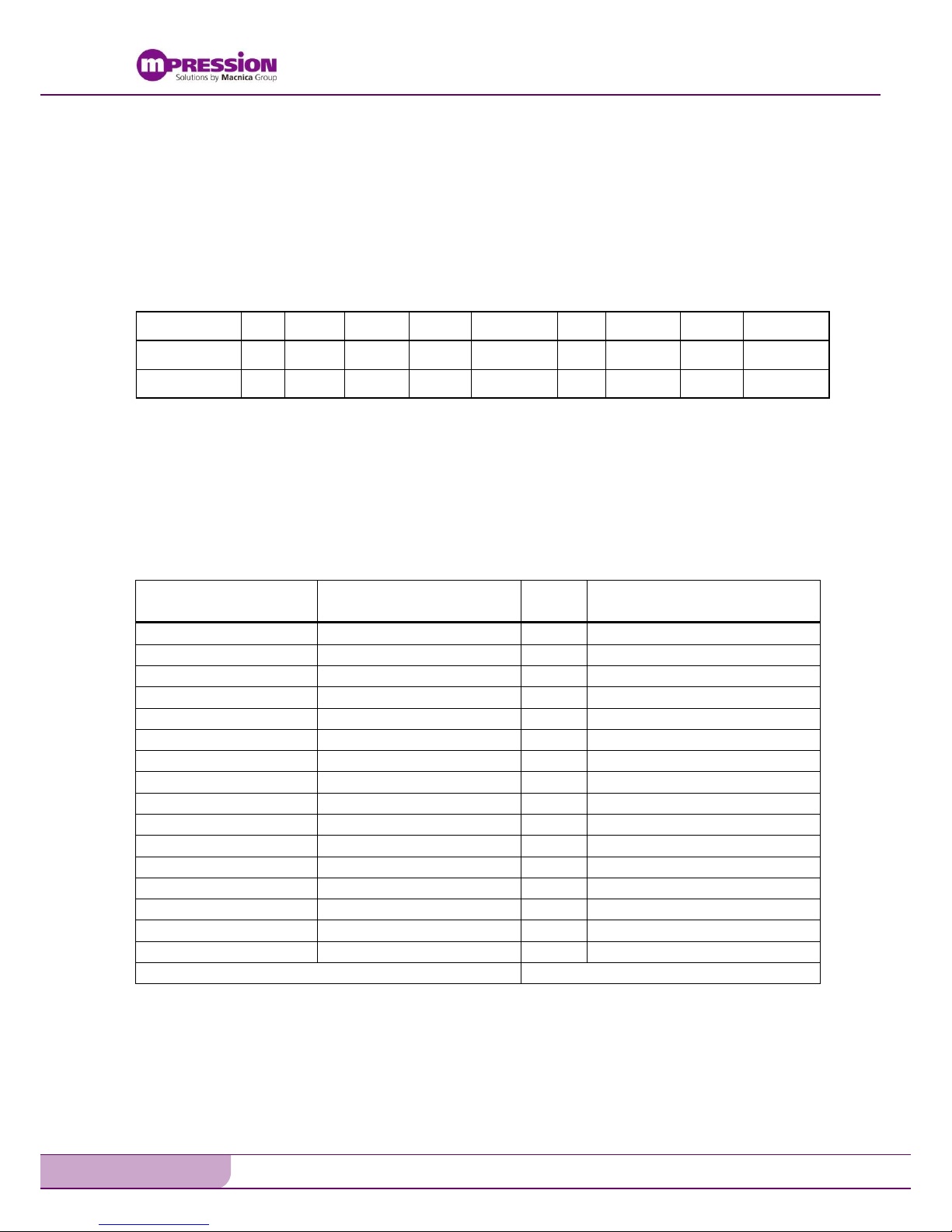
Table 2-1-1. Packing list
Customer letter
The Helio board
microSD card
USB Standard-A to Mini-B plug cable
AC adaptor (Output 12V/3.8A)
This Reference Manual
Download these files from Web site
described in the Customer letter.
The Helio board circuit diagram
FPGA sample design
If there is any question or doubt about the packaged product, contact your local distributor.

Mpression Helio Board
Reference Manual - Mpression Helio Board 9
© Mpression by Macnica Group
3. The Helio Board Hardware
Descriptions
3.1 Overview
This document describes the hardware features of the Helio board, including the detailed pin-out
and component reference information required to create custom FPGA designs that interface with
all components of the board.
Main CORE of the Helio board is Altera®Cyclone®V SoC. Altera Cyclone V SoC include the Hard
Processor System (HPS) with integrated ARM®Cortex™-A9MPCore processor.
One High-speed Mezzanine Card (HSMC) connector is available to add additional functionalities
via a variety of HSMCs available from various partners.
For more information on the following topics, refer to the respective documents:
As for Cyclone V device family, refer to the Cyclone V Device Handbook.
For HSMC Specification, refer to the High Speed Mezzanine Card (HSMC) Specification.
3.2 Key Components
The Helio board features the following key component blocks:
Key components are listed in Table 3-2-1.
Table 3-2-1. Key components
Supplier
Function Name
Part number
CPU
Altera
SoC with FPGA
5CSXFC6C6U23C8NES(*1)
5CSXFC5C6U23C7N(*2)
Configuration ROM
Altera
Configuration device
EPCQ256SI16N
CPLD
Altera
On-board USB-Blaster®II
EPM570GF100C5N
ROM
Microchip
EEPROM
24LC32A
RAM
Micron
DDR3-SDRAM
MT41J256M16RE
Ethernet
Micrel
Gigabit Ethernet PHY
KSZ9021RN
USB
SMSC(Microchip)
OTG USB PHY
USB3300-EZK
Cypress
USB PHY for USB-Blaster II
CY7C68013A-56BAXC
Real Time Clock
MAXIM
I2C Real time clock
DS1339C-33#
UART
Silicon Labs
USB to UART bridge
CP2103GM
Connector
TE Connectivity
Mictor for HPS
2-5767004-2
Samtec
HSMC
ASP-122953-01
Note: *1) 5CSXFC6C6U23C8NES was mounted in the Helio board Rev1.3 or earlier.
*2) 5CSXFC5C6U23C7N is mounted in the Helio board Rev1.4 or later.

Mpression Helio Board
10 Reference Manual - Mpression Helio Board
© Mpression by Macnica Group
3.3 Block Diagram
Figure 3-3-1 shows a block diagram of the Helio board.
Figure 3-3-1. The Helio board Block Diagram
Board Specification
Table 3-3-1. Board specification
PCB Size
Height
Width
100mm
167mm
PCB thickness
1.6mm
Layer number
8 Layers
256MB
DDR3-SDRAM
LVDS/
Single-Ended
Embedded
USB-Blaster II
Type-miniB
USB2.0 Mictor connector
(for HPS)
64MB
QSPI FlashROM
(Not mount)
Gigabit Ethernet
PHY
USB2.0
OTG (On The Go)
32kB
EEPROM
Real Time Clock
UART
(USB to UART bridge)
Push Button
(Re-Config)
Push Button Switch
(Cold, Warm reset)
DIP Switch
(User defined)
DIP Switch
(User defined)
GPIO
(TH)
LEDs
2x16 Char LCD
Header
1GB
DDR3-SDRAM
JTAG_Chain
x 4
x 1
x 4
Ref. cloclk
x32
x 2
SPI
x80
CLKIN x 3
CLK OUT x 3
: FPGA-side peripherals
: HPS-side peripherals
I2C
5CSXFC6C6U23(672pin)
ALTERA
Cyclone V SX SoC
5CSXFC6C6U23C8NES
rev1.3 or earlier
/
5CSXFC5C6U23C7N
rev1.4 or later
Push Button Switch
(User defined)
Configuration ROM
Push Button
(User defined)
x 4
x 3
Fixed OSC
50/100/125MHz x 4
LTC power Monitor
Micro SD Slot
x 4
x 4
x 4
Mpression Helio Board
Reference Manual - Mpression Helio Board 11
© Mpression by Macnica Group
4. The Helio board Components
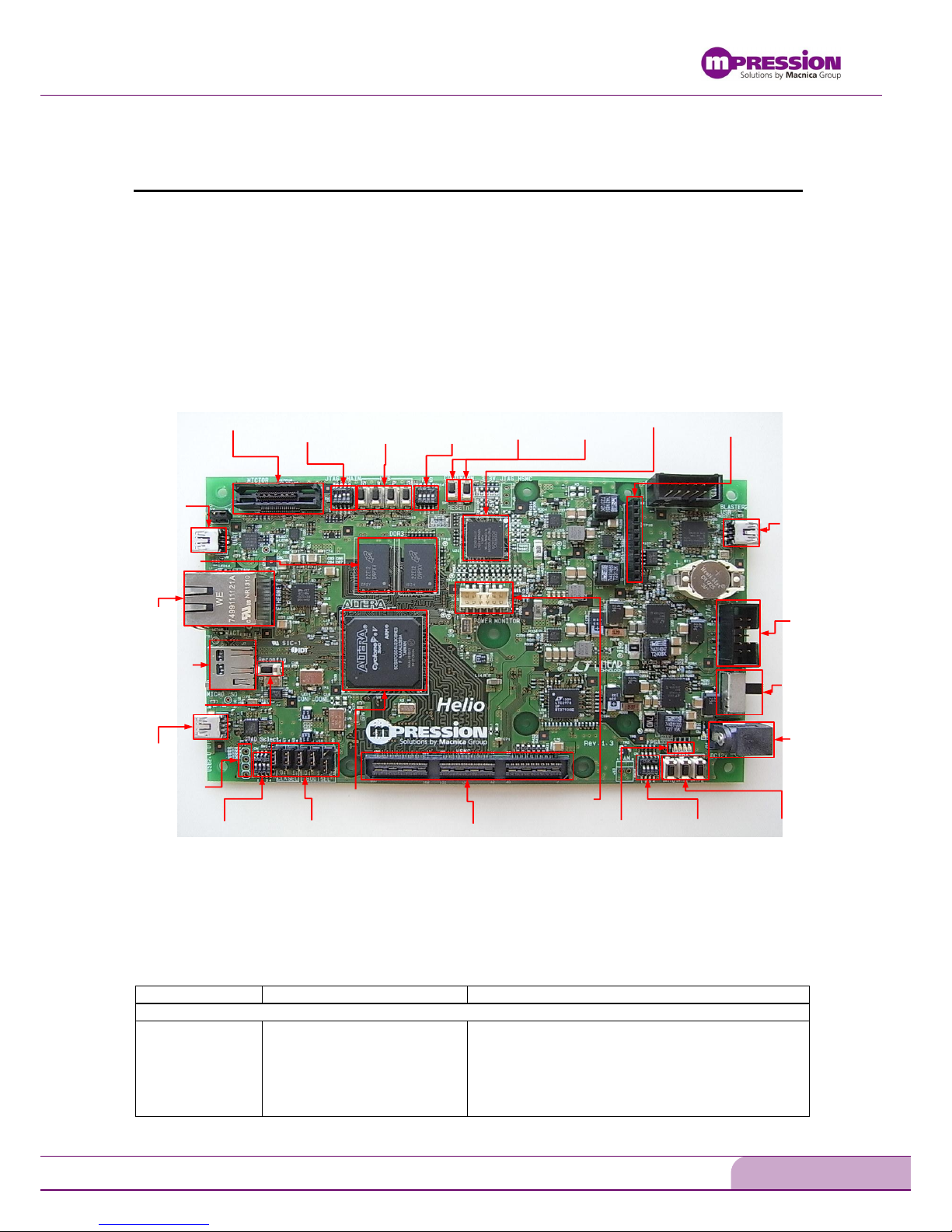
4.1 Board Overview
This section provides an overview of the Helio board Figure 4-1-1 shows a top view of the board.
Figure 4-1-1. Board top view
Table 4-1-1 describes the components and lists their corresponding board references.
Table 4-1-1. Board components
Board Reference
Type
Description
Featured Devices
U1
SoC
Cyclone V SoC, 5CSXFC6C6U23C8NES or
5CSXFC5C6U23C7N, 672-pin UBGA.
5CSXFC6C6U23C8NES was mounted in the
Helio board Rev1.3 or earlier.
5CSXFC5C6U23C7N is mounted in the Helio
board Rev1.4 or later.
Warm Reset
Push Button
(SW6)
MAXII CPLD
(U31)
Cold Reset
Push Button
(SW5)
User Defined
Dip Switch
For HPS
(SW14)
User Defined
Push Button
For HPS
(SW7-SW10)
JTAG Master
Select DIP Switch
(SW4)
JTAG 10pin
Header
(J2)
HSMC Port
(J4)
Cyclone V SX SoC (U1)
MICTOR_38P
Port (J1)
UART Port
(J9)
Gigabit
Ethernet
Port (J9)
Micro SD
Socket Port
(J7)
DDR3-SDRAM
(x32bit)
(U16, U17)
Character
LCD Port
(J8)
On Board USB
Blaster II Port
(J11)
USB 2.0 OTG
Port (J6)
User GPIO TH
(GPIO057,
58,59,61)
JTAG Chain Setting
DIP Switch (SW1)
Re-configuration
Push Button
(SW3)
HPS SettingJumper
(J16-J20)
User DIP Switch
For FPGA
(SW15)
User Push Button
For FPGA
(SW11-SW13)
DC Input Jack
(J14)
User LEDs
(LED3-LED6)
Power Monitor
Port (J15)
Power switch
(SW16)
*Power switch
is not mounted
in Rev1.2
Mpression Helio Board
12 Reference Manual - Mpression Helio Board
© Mpression by Macnica Group
U31
CPLD
MAX®II CPLD, EPM570GF100C5N, 100-pin FBGA
Configuration, Status, and Setup Elements
J2
JTAG 10pin header
Provides access to the JTAG chain and disables the
embedded USB-Blaster II when using an external
USB-Blaster cable.
SW1
JTAG chain control DIP
Switch
Remove or include devices in the active JTAG chain.
SW4
JTAG master select DIP
Switch
Select master I/F of JTAG chain, and master I/F for
HPS.
J11
USB type-B connector
USB interface for FPGA programming and debugging
thorough the embedded USB-Blaster II JTAG via a
type-B cable.
J16, J17, J18,
J19, J20
HPS setting Jumper switch
Selects for the HPS boot source, and the clock mode.
SW3
Re-configuration push button
FPGA reconfigured by the configuration ROM
(EPCQ) when pushed SW3.
SW5
Cold reset push button
Cold reset: HPS and Ethernet are reset when pushed
SW5.
SW6
Warm reset push button
Warm reset: Only HPS is reset when pushed SW6.
LED1
Configuration done LED
Illuminates when the FPGA is configured.
LED2
Cold reset LED
Illuminates when the HPS is Cold reset.
LED7
UART Transmit LED
Blink when there is UART data to transmit.
LED8
UART Receive LED
Blink when there is data on the UART receive buffer.
LED14
Ethernet LINK LED
Illuminates when the Ethernet linked.
LED15
Ethernet ACT LED
Illuminates when the Ethernet activity.
Clock Circuitry
U6
100-MHz oscillator
100.000-MHz crystal oscillator for the GXB reference
clock.
X1
50-MHz oscillator
50.000-MHz crystal oscillator for general purpose
logic.
X2
25-MHz oscillator
25.000-MHz crystal oscillator for the HPS primary
and secondary clock.
X3
100-MHz oscillator
100.000-MHz crystal oscillator for general purpose
logic.
X4
125-MHz oscillator
125.000-MHz crystal oscillator for general purpose
logic.
General User Input / Output
LED3, LED4,
LED5, LED6
User LEDs
Four user LEDs. Illuminates when driven low.
SW7, SW8, SW9,
SW10
User push button for HPS
Four user push buttons. Connected to the GPIO on
the HPS.
SW11, SW12,
SW13
User push button for FPGA
Three user push buttons. Connected to the IO of the
FPGA.
SW14
User DIP switch for HPS
Four-bit DIP switch. Connected to the GPIO of the
HPS.
SW15
User DIP switch for FPGA
Four-bit DIP switch. Connected to the IO of the
FPGA.
GPIO1, GPIO2,
GPIO3, GPIO4
User GPIO
Four GPIO through holes. Connected to the GPIO of
the HPS.
Memory Devices
U16, U17
DDR3-SDRAM
1GB DDR3-SDRAM (Two 512MB DDR3): Connected
to HPS with a 32-bit data bus.
U21
QSPI-Flash memory
64MB QSPI NOR Flash memory: Connected to HPS.
HPS support serial, Dual, Quad I/O SPI protocols.
Note: QSPI FlashROM was not mounted in the Helio
board.
U7
FPGA configuration ROM
Serial or quad-serial FPGA configuration in devices
that support active serial ASx1 or ASx4 configuration
schemes. 256-Mbit.
U19
EEPROM
32-kbit I2C Serial EEPROM. Connected to HPS
Communication Ports

Mpression Helio Board
Reference Manual - Mpression Helio Board 13
© Mpression by Macnica Group
J1
Mictor connector
The ARM DSTREM or third party debugger is able to
connect to Mictor connector.
J4
HSMC port
Provides 84CMOS or 17LVDS channels per the
HSMC specification.
J5
Gigabit Ethernet port
RJ-45 connector which provides a 10/100/1000
Ethernet connection via a Micrel KSZ9021RL and the
HPS-based Ethernet MAC in RGMII mode.
J6
USB 2.0 OTG port
USB mini-AB connector which provides a USB2.0
Hi-Speed and OTG protocol via a SMSC USB3300
and the HPS-based USB2.0 LINK in ULPI.
J7
Micro SD socket
Micro SD socket which provides a Micro SD via the
HPS-based SD/SDIO/MMC flash controller.
J9
UART port
USB mini-B connector which provides a USB-serial
via a Silicon Labs CP2103 and the HPS-based UART.
J11
On-Board USB-Blaster II port
USB mini-B connector which provides the FPGA
configuration via a Cypress CY7C68013A and an
Altera MAXII CPLD.
Display Interface
J16
Character LCD
Connector that interfaces to a provided 16character
x2 line LCD module along with two standoffs.
Power Supply
J14
DC input jack
Accepts a 12-V DC power supply.
SW16
Power switch
SW16 is the slide switch for power supply ON/OFF.
(However, SW16 is not mounted on the Helio Rev1.2
board. The power supply of the Helio Rev1.2 board is
supplied by connecting an AC adapter.)
Mpression Helio Board
14 Reference Manual - Mpression Helio Board
© Mpression by Macnica Group
4.2 Featured Device: Cyclone V SoC
Cyclone V SoC 5CSXFC6C6U23CNES and 5CSXFC5C6U23C7N device in a 672-pin UBGA
package is surface-mounted on the Helio board.
Table 4-2-1 describes the features of the Cyclone V SoC 5CSXFC6C6U23C and 5CSXFC5C6U23C
device.
Table 4-2-1. Cyclone V SoC Features
4.2.1 I/O Resources
The Cyclone V SoC 5CSXFC6C6U23CNES and 5CSXFC5C6U23C7N device has 342 user I/Os and
six transceiver channels. Table 4-2-2 lists the Cyclone V SoC device I/O pin count and usage by
function on this board.
Table 4-2-2. Cyclone V SoC Device I/O Pin Count
Function
I/O Standard
I/O
Count
Special Pins
DDR3-SDRAM
1.5-V SSTL
80
HPS, One differential x4 DQS pin
QSPI FlashROM
3.3-V CMOS
6
HPS
USB2.0 OTG port
3.3-V CMOS
12
HPS
UART
3.3-V CMOS
2
HPS
RTC & EEPROM
3.3-V CMOS
2
HPS (I2C)
Character LCD
3.3-V CMOS
4
HPS
Gigabit Ethernet port
3.3-V CMOS
15
HPS
Push buttons
3.3-V CMOS
2
HPS
Dip switches
3.3-V CMOS
4
HPS
GPIO
3.3-V CMOS
4
HPS
HSMC port
2.5-V CMOS + LVDS
91
17 LVDS, I2C
On-board USB-Blaster II
1.5-V
17
-
Push buttons
2.5-V CMOS
5
User defined, Re-config for FPGA
Dip switches
2.5-V CMOS
4
User defined
LEDs
2.5-V CMOS
4
User defined
Clock or Oscillators
2.5V CMOS + LVDS + PCML
16
Total I/O Used:
268
Device ALMs
Equivalent
LEs
M10K RAM
Blocks
Total RAM
(Kbits)
18-bit x 18-bit
multipliers
PLLs Transceivers
ARM
Cortex-A9
Pakage Type
5CSXFC6C6U23C 41,509 110,000 557 5,570 224
FPGA 6
HPS 3
6 Dual-core 672-pin UBGA
5CSXFC5C6U23C 32,075 85,000 397 3972 174
FPGA 6
HPS 3
6 Dual-core 672-pin UBGA

Mpression Helio Board
Reference Manual - Mpression Helio Board 15
© Mpression by Macnica Group
4.3 JTAG Configuration
This section describes configuration methods of FPGA and HPS supported by the Helio board. The
Helio board supports the following three configuration methods:
On-board USB-Blaster II is the default method for configuring the FPGA/HPS using the
Quartus®II Programmer/the ARM DS-5™Altera Edition in JTAG mode with the supplied
USB cable.
Mictor connector is the default method for debugging the HPS using the In-Circuit Emulator
in JTAG mode.
External USB-Blaster for configuring the FPGA/HPS using an external USB-Blaster that connects
to the JTAG chain header (J2).
4.3.1 HPS debugging and FPGA Programming over On-board
USB-Blaster II
This configuration method is implemented using USB-mini type-B connector (J11), a USB 2.0 PHY
device (U33), and an Altera MAX II CPLD EPM570GF100C5N (U31). Connect the USB cable
directly to the USB-Blaster II port of the Helio board.
HPS can be debugged via ARM DS-5 Altera Edition. And FPGA can be programmed via Quartus II
programmer. The On-board USB-Blaster II is normally masters of the JTAG chain. Figure 4-3-1
illustrates the JTAG chain.
Figure 4-3-1. JTAG Chain
The JTAG setting control DIP switch (SW1, SW4) controls the Analog Switch and the Multiplexer
shown in Figure 4-3-1. Refer to 4.5.1 JTAG settings DIP switch if you want to confirm detail
settings for JTAG setting DIP switches.
GPIO
On-Board
USB
-
BlasterII
GPIO
GPIO
GPIO
Cyclone V SoC
FPGA
TCK
TMS
TDI
TDO
JTAG Slave
JTAG Master
TCK
TMS
TDO
GPIO
TDI
HPS_TCK
HPS_TMS
HPS_TDI
HPS_TDO
HPS Side
Bank 7A
HPS_TRST
TCK
Mictor 38P
TMS
TDO
JTAG Master
TDI
TRST
TCK
JTAG 10P
TMS
TDO
JTAG Master
TDI
TRST
Disable
Enable
MUX
TCK
MUX
TMS
TDO
TDI
R
R
Ana log
Switch
TCK
TMS
TDO
TDI
DI P Swi tch
Enable
DI P Swi tch
MICTOR_TRST
MICTOR_TRST
JTAG_TRST
JTAG_TRST
3.3V
3.3V
3.3V
2.5V
VCCIO7A_HPS
3.3V
VCCPD3A
VCCIO3A
FPGA Side
Bank 3A
Analog Switch TS5A23157 supply
voltage = 3.3V
Ana log
Switch
Ana log
Switch
Anal og
Swi tch
3.3V
3.3V
GPIO
Mpression Helio Board
16 Reference Manual - Mpression Helio Board
© Mpression by Macnica Group
4.3.2 HPS debugging over Mictor connector for In-Circuit Emulator
Mictor connector (J1) is the connector that has JTAG and Trace data 8-bit bus for HPS debugging
with In-Circuit Emulator of ARM coretex-A9.
JTAG and Trace data 8-bit bus of HPS is connected to Mictor connector when JTAG setting DIP
switch SW1-[2] was OFF. Refer to 4.5.1 JTAG settings DIP switchif you want to confirm detail
settings for JTAG setting DIP switches.
Table 4-3-1 shows the Mictor connector pin assignments.
Table 4-3-1. Mictor Connector Pin Assignments
Board
Reference(J4)
Schematic
Signal Name
I/O Standard
Cyclone V SoC
Pin Number
Description
6
TRACE_CLK_MIC
3.3-V
C21
Trace Clock
9
MICTOR_RSTn
3.3-V
A23
HPS Reset
11
JTAG_MICTOR_TDI
3.3-V
D22
JTAG Data Input
15
JTAG_MICTOR_TCK
3.3-V
H22
JTAG Clock
16
TRACE_DATA7
3.3-V
C18
Trace Data Bit 7
17
JTAG_MICTOR_TMS
3.3-V
A29
JTAG Mode Select
18
TRACE_DATA6
3.3-V
A19
Trace Data Bit 6
19
JTAG_MICTOR_TDO
3.3-V
B23
JTAG Data Output
20
TRACE_DATA5
3.3-V
J18
Trace Data Bit 5
21
MICTOR_TRST
3.3-V
C22
JTAG Reset
22
TRACE_DATA4
3.3-V
A20
Trace Data Bit 4
24
TRACE_DATA3
3.3-V
K18
Trace Data Bit 3
26
TRACE_DATA2
3.3-V
A21
Trace Data Bit 2
28
TRACE_DATA1
3.3-V
B21
Trace Data Bit 1
38
TRACE_DATA0
3.3-V
A22
Trace Data Bit 0
4.3.3 FPGA Programming over External USB-Blaster
The JTAG header (J2) provides another method for configuring the FPGA using an external
USB-Blaster device with the Quartus II Programmer running on a PC. To prevent contention
between the JTAG masters, the On-board USB-Blaster II is automatically disabled when you
connect an external USB-Blaster to the JTAG chain through the JTAG header (J2). Table 4-3-2 lists
the JTAG header pin assignment.
Table 4-3-2. JTAG header Pin Assignments
Board
Reference
(J2)
Schematic
Signal Name
I/O Standard
Cyclone V
SoC
Pin Number
Description
1
JTAG_TCK
3.3-V
―
JTAG Clock
2
USB_DISABLEn
3.3-V
―
On-board USB-Blaster II disable
when JTAG header is used,
the On-board USB-Blaster II
JTAG interface cannot be used.
3
JTAG_BLASTER_TDI
3.3-V
―
JTAG Data from device
4
3.3V
―
―
3.3V Power
Mpression Helio Board
Reference Manual - Mpression Helio Board 17
© Mpression by Macnica Group
5
JTAG_TMS
3.3-V
―
JTAG Mode Select
6
MICTOR_RSTn
3.3-V
―
Mictor Reset Signal Input
7
8
JTAG_TRST
3.3-V
―
JTAG Reset
9
JTAG_BLASTER_TDO
3.3-V
―
JTAG Data to device
10
GND
―
―
Ground
Mpression Helio Board
18 Reference Manual - Mpression Helio Board
© Mpression by Macnica Group
4.4 Status Elements
The Helio board includes status LEDs. This section describes the status elements.
Table 4-4-1 lists the LED board references, name, and functional descriptions.
Table 4-4-1. Board-Specific LEDs
Board
Reference
Schematic
Signal Name
I/O Standard
Description
LED1
CONF_DONE(Inverted)
3.3-V
Green LED. Illuminates when FPGA
is successfully configured.
LED2
COLD_RESETn
3.3-V
Red LED.
Illuminates when cold_reset is asserted.
LED13
5.0V (Power)
5.0-V
Green LED.
Illuminates when 5.0V power is active.
Mpression Helio Board
Reference Manual - Mpression Helio Board 19
© Mpression by Macnica Group
4.5 Setup Elements
The Helio board includes some of setup elements. This section describes the following setup
elements:
JTAG settings DIP switch
HPS operation mode setting Jumper
HPS reset push button
Program configuration push button
MSEL pins settings
4.5.1 JTAG settings DIP switch
The JTAG setting control DIP switch (SW1, SW4) remove or include devices in the active JTAG
chain and select JTAG master interface. Table 4-5-1, Table 4-5-2 lists the switch controls and its
descriptions.
Table 4-5-1. JTAG Setting Control DIP Switch (SW1)
Board
Reference
Schematic
Signal Name
I/O Standard
Description
Default
SW1-1
JTAG_SEL
3.3-V
JTAG master interface select:
ON : Select On-board USB-Blaster II
or JTAG 10pin Header
OFF : Select MICTOR connector
ON
SW1-2
JTAG_HPS_SEL
3.3-V
Cyclone V SoC HPS JTAG Master Select:
ON : Select On-board USB-Blaster II
or JTAG 10pin Header
OFF : Select MICTOR connector
ON
SW1-[3:4]
-
-
This switch has to set ON when normal
operation.
ON
Table 4-5-2. JTAG Setting Control DIP Switch (SW4)
Board
Reference
Schematic
Signal Name
I/O Standard
Description
Default
SW4-1
HPS_JTAG_EN
3.3-V
Remove or include HPS side in the active JTAG
chain:
ON : Bypass Cyclone V SoC HPS Side
OFF : Cyclone V SoC HPS Side in-chain
OFF
SW4-2
FPGA_JTAG_EN
3.3-V
Remove or include FPGA side in the active JTAG
chain:
ON : Bypass Cyclone V SoC FPGA Side
OFF : Cyclone V SoC FPGA Side in-chain
OFF
SW4-[3:4]
-
-
This switch has to set ON when normal operation.
ON

Mpression Helio Board
20 Reference Manual - Mpression Helio Board
© Mpression by Macnica Group
4.5.2 HPS operation mode settings Jumper
The HPS operation mode setting Jumpers are Jumper for the Cyclone V SoC HPS side BSEL[2:0]
and CSEL[1:0]. Table 4-5-3 shows the HPS operation mode setting Jumper.
Table 4-5-3. HPS operation mode setting Jumper
Board
Reference
Schematic
Signal Name
I/O Standard
Description
J16
SPI_CSn
(BOOTSEL0)
3.3-V
boot select BSEL0:
Jumper setting
BSEL0
Default
1-2 short
High(1)
1-2 short
2-3 short
Low(0)
J18
QSPI_SS0
(BOOTSEL1)
3.3-V
boot select BSEL1:
Jumper setting
BSEL1
Default
1-2 short
High(1)
2-3 short
2-3 short
Low(0)
J20
BOOTSEL2
3.3-V
boot select BSEL2:
Jumper setting
BSEL2
Default
1-2 short
High(1)
1-2 short
2-3 short
Low(0)
J17
UART_TX
(CLKSEL0)
3.3-V
clock select CSEL0:
Jumper setting
CSEL0
Default
1-2 short
High(1)
2-3 short
2-3 short
Low(0)
J19
CLKSEL1
3.3-V
clock select CSEL1:
Jumper setting
CSEL1
Default
1-2 short
High(1)
2-3 short
2-3 short
Low(0)
For more information on the BSEL and CSEL of HPS, refer to the following document:
Booting and Configuration of Cyclone V SoC HPS, refer to the cv_5400A.
4.5.3 HPS reset push button
The HPS reset push button, COLD_RESETn (SW5) and WARM_RESETn (SW6), are input to the
Cyclone V SoC HPS_PORn and HPS_nRST pin. Table4-5-4 lists the button controls and its
descriptions.
Table of contents
Popular Motherboard manuals by other brands


VIA Technologies
VIA Technologies EPIA-N701 user manual

Renesas
Renesas RL78 Series user manual

Connect One
Connect One II-EVB-363MW user manual

Texas Instruments
Texas Instruments Stellaris EK-LM3S9B92 user manual

American Megatrends
American Megatrends Baby Screamer LC user guide

Biostar
Biostar U8788 Bios setup manual


