MSI MS-98J8 User manual

i
MS-98J8
(v1.x) Industrial Computer Board

ii
Preface MS-98J8
Copyright and Trademarks Notice
Copyright © Micro-Star Int’l Co., Ltd. All rights reserved. The MSI logo used is
a registered trademark of Micro-Star Int’l Co., Ltd. All other marks and names
mentioned may be trademarks of their respective owners. No warranty as to
accuracy or completeness is expressed or implied. MSI reserves the right to
make changes to this document without prior notice.
Revision History
Revision Date
V1.2 2020/09
Technical Support
If a problem arises with your product and no solution can be obtained from
the user’s manual, please contact your place of purchase or local distributor.
Alternatively, please visit https://www.msi.com/support/ for further guidance.

iii
Preface MS-98J8
Safety Instructions
■Always read the safety instructions carefully.
■Keep this User’s Manual for future reference.
■Keep this equipment away from humidity.
■Lay this equipment on a reliable at surface before setting it up.
■The openings on the enclosure are for air convection hence protects the
equipment from overheating. DO NOT COVER THE OPENINGS.
■Make sure the voltage of the power source and adjust properly 110/220V
before connecting the equipment to the power inlet.
■Place the power cord such a way that people can not step on it. Do not place
anything over the power cord.
■Always Unplug the Power Cord before inserting any add-on card or module.
■All cautions and warnings on the equipment should be noted.
■Never pour any liquid into the opening that could damage or cause electrical
shock.
■If any of the following situations arises, get the equipment checked by
service personnel:
▶The power cord or plug is damaged.
▶Liquid has penetrated into the equipment.
▶The equipment has been exposed to moisture.
▶The equipment does not work well or you can not get it work according
to User’s Manual.
▶The equipment has dropped and damaged.
▶The equipment has obvious sign of breakage.
■DO NOT LEAVE THIS EQUIPMENT IN AN ENVIRONMENT
UNCONDITIONED, STORAGE TEMPERATURE ABOVE 60oC, IT MAY
DAMAGE THE EQUIPMENT.

iv
Preface MS-98J8
Chemical Substances Information
In compliance with chemical substances regulations, such as the EU REACH
Regulation (Regulation EC No. 1907/2006 of the European Parliament and the
Council), MSI provides the information of chemical substances in products at:
https://www.msi.com/html/popup/csr/evmtprtt_pcm.html
Battery Information
European Union:
Batteries, battery packs, and accumulators should not be
disposed of as unsorted household waste. Please use the
public collection system to return, recycle, or treat them in
compliance with the local regulations.
廢電池請回收
Taiwan:
For better environmental protection, waste batteries should
be collected separately for recycling or special disposal.
California, USA:
The button cell battery may contain perchlorate material
and requires special handling when recycled or disposed
of in California.
For further information please visit:
https://www.dtsc.ca.gov/hazardouswaste/perchlorate/
Danger of explosion if battery is incorrectly replaced. Replace only with the
same or equivalent type recommended by the manufacturer.

v
Preface MS-98J8
CE Conformity
Hereby, Micro-Star International CO., LTD declares that this device
is in compliance with the essential safety requirements and other
relevant provisions set out in the European Directive.
FCC-B Radio Frequency
Interference Statement
This equipment has been tested and found to comply with
the limits for a Class B digital device, pursuant to Part 15 of the FCC Rules.
These limits are designed to provide reasonable protection against harmful
interference in a residential installation. This equipment generates, uses and can
radiate radio frequency energy and, if not installed and used in accordance with
the instruction manual, may cause harmful interference to radio communications.
However, there is no guarantee that interference will not occur in a particular
installation. If this equipment does cause harmful interference to radio or
television reception, which can be determined by turning the equipment o and
on, the user is encouraged to try to correct the interference by one or more of the
measures listed below:
■Reorient or relocate the receiving antenna.
■Increase the separation between the equipment and receiver.
■Connect the equipment into an outlet on a circuit dierent from that to
which the receiver is connected.
■Consult the dealer or an experienced radio/television technician for
help.
Notice 1
The changes or modications not expressly approved by the party responsible for
compliance could void the user’s authority to operate the equipment.
Notice 2
Shielded interface cables and AC power cord, if any, must be used in order to
comply with the emission limits.
This device complies with Part 15 of the FCC Rules. Operation is subject to the
following two conditions:
1) this device may not cause harmful interference, and
2) this device must accept any interference received, including interference that
may cause undesired operation.
WEEE Statement
Under the European Union (“EU”) Directive on Waste Electrical and
Electronic Equipment, Directive 2002/96/EC, which takes eect on
August 13, 2005, products of “electrical and electronic equipment”
cannot be discarded as municipal waste anymore and manufacturers
of covered electronic equipment will be obligated to take back such products at
the end of their useful life.

vi
Preface MS-98J8
CONTENTS
Copyright and Trademarks Notice................................................................. ii
Revision History ............................................................................................ ii
Technical Support.......................................................................................... ii
Safety Instructions.........................................................................................iii
Chemical Substances Information ............................................................... iv
Battery Information....................................................................................... iv
CE Conformity............................................................................................... v
FCC-B Radio Frequency Interference Statement ......................................... v
WEEE Statement .......................................................................................... v
1 Overview.......................................................................................1-1
Specications.............................................................................................1-2
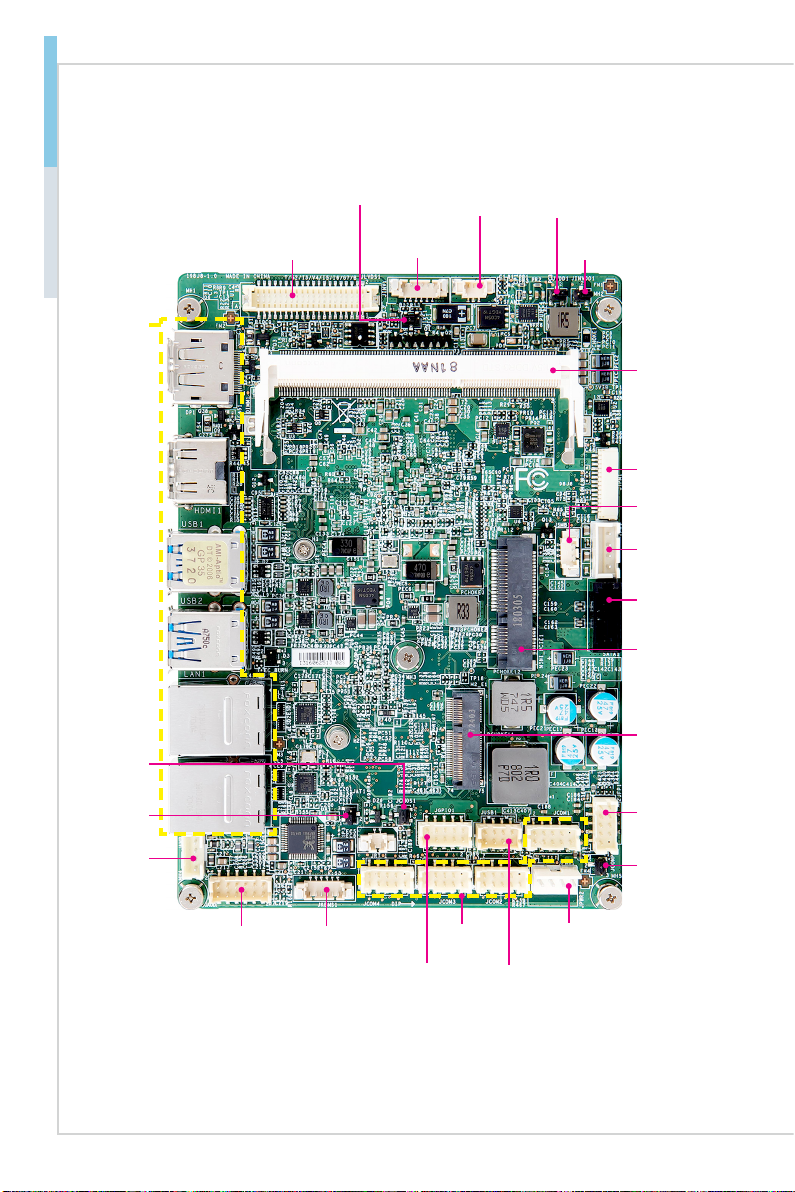
Layout ........................................................................................................1-4
2 Hardware Setup ...........................................................................2-1
Memory ......................................................................................................2-3
Power Supply.............................................................................................2-4
Rear Panel I/O ...........................................................................................2-5
Connector...................................................................................................2-6
Jumper .....................................................................................................2-12
Slot...........................................................................................................2-14
3 BIOS Setup...................................................................................3-1
Entering Setup ...........................................................................................3-2
The Menu Bar ............................................................................................3-4
Main ...........................................................................................................3-5
Advanced ...................................................................................................3-6
Boot..........................................................................................................3-12
Security ....................................................................................................3-13
Chipset.....................................................................................................3-18
Power .......................................................................................................3-19
Save & Exit...............................................................................................3-21
Appendix GPIO WDT BKL Programming ...................................... A-1
Abstract..................................................................................................... A-3
General Purposed IO ................................................................................ A-4
Watchdog Timer ........................................................................................ A-5
LVDS Backlight Brightness Control........................................................... A-6
SMBus Access .......................................................................................... A-7

1-1-1
Thank you for choosing the MS-98J8, an excellent industrial computer
board.
Based on the innovative Intel®Apollo Lake Series Processor, the MS-
98J8 is engineered to provide reliable performance for a wide variety of
industrial applications.
1Overview

1-2
Overview MS-98J8
Specications
Processor
■Intel® Celeron® J3455 QC 1.5/2.3GHz (Burst)
■Intel® Celeron® N3350 DC 1.1/2.4GHz (Burst)
■Intel® Atom™ X5-E3940 QC 1.6/1.8GHz (Burst)
Memory
■1x DDR3L 1866/1600 MHz SO-DIMM slot
■Up to 8GB
Network
■2 x Realtek RTL8111H GbE LAN (Co-lay RTL8111G)
Storage
■1x SATA 6Gb/s port
■1x mSATA slot (shared with Mini-PCIe slot)
Audio
■Realtek ALC887 audio codec, Co-lay ALC888S
■1 x front audio header
■1 x amplier header
Graphics
■Graphics integrated in Intel processor
-DisplayPort, HDMI, LVDS
Expansion Slot
■1 x Mini-PCIe slot (shared with mSATA )
■1 x M.2 E-Key 2230 slot (with USB2.0 signal)
Important
MS-98J8 only supports installing ONE WiFi / BT module. Please install your
WiFi / BT module to Mini-PCIe slot or M.2 E Key slot.
Rear Panel I/O
■1 x DisplayPort
■1 x HDMI port
■4 x USB 3.2 Gen 1 ports
■2 x RJ45 GbE LAN ports

1-3
Overview MS-98J8
Internal I/O
■1x DC power connector
■1x system fan connector
■1 x SATA 6Gb/s port
■1 x SATA power connector
■1 x USB2.0 connector
■1 x front panel connector
■1 x front audio connector
■1 x amplier connector
■1 x GPIO connector
■1 x keyboard/mouse connector
■1 x SMBus connector
■1 x LPC connector
■4 x serial port connectors
■1 x LVDS connector
■1 x LVDS inverter connector
■1 x LVDS power jumper
■1 x LVDS inverter power jumper
■1x clear CMOS jumper
■1 x serial port power jumper
■1 x AT/ATX jumper
■1 x TXE jumper
Form Factor
■Form Factor: 102mm x 146mm
Environment
■Operating Temperature: -10 ~ 60oC
■Storage Temperature: -20 ~ 80oC
■Humidity: 10 ~ 90% RH, non-condensing

1-4
Overview MS-98J8
Layout
Front Audio
Connector
Mini-PCIe/
mSATA Slot
Clear CMOS
Jumper
AT/ATX
Jumper
SO-DIMM Slot
COM Port
Connector
USB 2.0
Connector
LVDS Inverter
Connector
SATA 3.0
Connector
GPIO
Connector
System Fan
Connector
LVDS
Connector
COM Port
Power Jumper
LPC Connector
Front Panel
Connector
SATA Power
Connector
Amplier
Connector
LVDS Power
Jumper
Keyboard/Mouse
Connector
M.2 Slot
LVDS Inverter
Power Jumper
SMBus
Connector
DC Power
Connector
TXE Jumper
Rear Panel
I/O

2-2-1
This chapter provides you with the information about hardware
setup procedures. While doing the installation, be careful in holding
the components and follow the installation procedures. For some
components, if you install in the wrong orientation, the components will
not work properly.
Use a grounded wrist strap before handling computer components. Static
electricity may damage the components.
2Hardware Setup

2-2
Hardware Setup MS-98J8
Components Reference Guide
Memory..............................................................................................2-3
Power Supply....................................................................................2-4
DC Power Connector: JPWR1...................................................................2-4
SATA Power Connector: JPW1 ..................................................................2-4
Rear Panel I/O ...................................................................................2-5
Connector..........................................................................................2-6
Fan Power Connector: SYSFAN1 ..............................................................2-6
GPIO Connector: JGPIO1..........................................................................2-6
USB2.0 Connector: JUSB1........................................................................2-6
Front Panel Connector: JFP1.....................................................................2-7
LPC Debug Port Connector: JTPM1..........................................................2-7
Serial ATA Connector: SATA1 ....................................................................2-7
LVDS Inverter Connector: JINV1 ...............................................................2-8
LVDS Connector: JLVDS1 .........................................................................2-8
Serial Port Connector: JCOM1 ~ JCOM4 ..................................................2-9
Audio Amplier Pinheader: JAMP1 ..........................................................2-10
Front Audio Connector: JAUD1................................................................2-10
PS/2 Keyboard/Mouse Connector: JKBMS1............................................ 2-11
SMBus Connector: JSMB1 ...................................................................... 2-11
Jumper.............................................................................................2-12
Clear CMOS Jumper: JCMOS1 ...............................................................2-12
AT/ATX Jumper: JAT1..............................................................................2-12
Serial Port Power Jumper: JCOMP1........................................................2-13
TXE Jumper: JTXE1 ................................................................................2-13
LVDS Power Jumper: JVDD1 ..................................................................2-13
LVDS Inverter Power Jumper: JINVDD1..................................................2-13
Slot...................................................................................................2-14
Mini-PCIe (Peripheral Component Interconnect Express) Slot................2-14
M.2 Slot (Key E, 2230).............................................................................2-14

2-3
Hardware Setup MS-98J8
Memory
The SO-DIMM slot is intended for memory modules.
1. Locate the SO-DIMM slot. Align
the notch on the DIMM with the
key on the slot and insert the
DIMM into the slot.
2. Push the DIMM gently
downwards until the slot levers
click and lock the DIMM in
place.
3. To uninstall the DIMM, ip the slot levers outwards and the DIMM will be
released instantly.
Important
You can barely see the golden nger if the DIMM is properly inserted in the
DIMM slot.

2-4
Hardware Setup MS-98J8
Power Supply
DC Power Connector: JPWR1
This connector allows you to connect a 9~36V DC power adapter.
4.Ground
3.Ground
2.DC Power
1.DC P
ower
SATA Power Connector: JPW1
This connector is used to provide power to SATA devices.
Important
Make sure all power connectors are connected to the power supply to ensure
stable operation of the motherboard.

2-5
Hardware Setup MS-98J8
Rear Panel I/O
USB 3.2 Gen 1 Ports
DisplayPort GbE RJ45 Port
HDMI Port
hDisplayPort
DisplayPort is a digital display interface standard. This connector is used to
connect a monitor with DisplayPort inputs.
hHDMI Port
The High-Denition Multimedia Interface (HDMI) is an all-digital audio/video
interface capable of transmitting uncompressed streams. HDMI supports all TV
format, including standard, enhanced, or high-denition video, plus multi-channel
digital audio on a single cable.
hUSB 3.2 Gen 1 Port
The USB 3.2 Gen 1 port is backward-compatible with USB 2.0 devices and
supports data transfer rate up to 5 Gbit/s (SuperSpeed).
hGbE RJ45 Port
The standard single RJ45 LAN jack is provided for connection to the Local Area
Network (LAN). You can connect a network cable to it.
Speed LED Active
LED
LED LED Status Description
Active
LED
O No link
Yellow Linked
Blinking Data activity
Speed
LED
O 10 Mbps connection
Green 100 Mbps connection
Orange 1 Gbps connection

2-6
Hardware Setup MS-98J8
Connector
Fan Power Connector: SYSFAN1
The fan power connector supports system cooling fans with +12V. When
connecting the wire to the connectors, always note that the red wire is the positive
and should be connected to the +12V; the black wire is Ground and should be
connected to GND. If the motherboard has a System Hardware Monitor chipset
onboard, you must use a specially designed fan with speed sensor to take
advantage of the fan control.
GPIO Connector: JGPIO1
This connector is provided for the General-Purpose Input/Output (GPIO)
peripheral module.
USB2.0 Connector: JUSB1
This connector, compliant with Intel I/O Connectivity Design Guide, is ideal for
connecting high-speed USB interface peripherals such as USB HDD, digital
cameras, MP3 players, printers, modems and the like.
8.Power
3.USB-
1.Power
6.USB-
5.USB+
4.USB+
7.GND
2.GND
Important
Note that the pins of VCC and GND must be connected correctly to avoid possible
damage.

2-7
Hardware Setup MS-98J8
Front Panel Connector: JFP1
This front panel connector is provided for electrical connection to the front panel
switches & LEDs and is compliant with Intel Front Panel I/O Connectivity Design
Guide.
8.POWER SWITCH
3.HDD LED-
1.HDD LED+
6.POWER SWITCH
5.RESET SWIT CH
4.POWER LED-
7.RESET SWIT CH
2.POWER LED+
9.NC
LED(+) Voltage(V) Current(mA)
Power 5 18.51
HDD 5 18.51
LPC Debug Port Connector: JTPM1
This connector works as LPC debug port.
1.LPC_FRAME
#
2.LPC_AD3
3.LPC_AD2
4.LPC_AD1
5.LPC_AD0
6.L_LDRQ0#
7.TPM_CLK
8.SERIRQ_R
9.PLTRST_TPM#
10.VCC5
11.VCC3
12.GND
13.NA
14.GND
Serial ATA Connector: SATA1
This connector is a high-speed Serial ATA interface port. Each connector can
connect to one Serial ATA device.
Important
Please do not fold the SATA cable into a 90-degree angle. Otherwise, data loss
may occur during transmission.

2-8
Hardware Setup MS-98J8
LVDS Inverter Connector: JINV1
The connector is provided for LCD backlight options.
LVDS Connector: JLVDS1
The LVDS (Low Voltage Dierential Signal) connector provides a digital interface
typically used with at panels. After connecting an LVDS interface at panel to
the JLVDS1, be sure to check the panel datasheet and set the LVDS jumper to
proper power voltage.
39.LVDSB_CLK
#
27.LVDSB_DATA#1
25.LVDSB_DATA1
23.GND
21.LVDSA_DATA#3
19.LVDSA_DATA3
17.GND
15.LVDSA_DATA#1
13.LVDSA_DATA1
11.LVDS_BLON
9.L_BKLT_CTRL#
7.LVDS_DDC_CLK
5.LCD_VDD
3.LCD_VDD
1.+12V
40.
LVDSA_CLK#
28.LVDSB_DATA#0
26.
LVDSB_DATA0
24.GND
22.LVDSA_DATA#2
20.LVDSA_DATA2
18.GND
16.LVDSA_DATA#0
14.LVDSA_DATA0
12.LVDS_DETECT#_C
10.LVDS_VDD_EN
8.
LVDS_DDC_DATA
6.LCD_VDD
4.+12V
2.+12V
37.LVDSB_CLK
35.GND
33.LVDSB_DATA#3
31.LVDSB_DATA3
29.GND
38.LVDSA_CLK
36.GND
34.LVDSB_DATA#2
32.LVDSB_DATA2
30.GND
Important
Pin 12 is a detect pin. When using a customized LVDS cable, pin 12 should be a
signal ground with a low impedance. Otherwise, LVDS will not function.

2-9
Hardware Setup MS-98J8
Serial Port Connector: JCOM1 ~ JCOM4
This connector is a 16550A high speed communications port that sends/
receives 16 bytes FIFOs. You can attach a serial device to it. JCOM1 supports
RS232/422/485. JCOM2~4 support RS232.
hJCOM1
8
3
1
6
5
4
7
2
9
RS232
PIN SIGNAL DESCRIPTION
1
2
3
4
5
6
7
8
9
DCD
RXD
TXD
DTR
GND
DSR
RTS
CTS
POWER
Data Carrier Detect
Receive Data
Transmit Data
Data Terminal Ready
Ground
Data Set Ready
Request To Send
Clear To Send
5V or 12V selected by Jumper
RS422
PIN SIGNAL DESCRIPTION
1
2
3
4
5
6
7
8
9
TXD-
TXD+
RXD+
RXD-
GND
NC
NC
NC
NC
Transmit Data, Negative
Transmit Data, Positive
Receive Data, Positive
Receive Data, Negative
Ground
No Connection
No Connection
No Connection
No Connection
RS485
PIN SIGNAL DESCRIPTION
1
2
3
4
5
6
7
8
9
D-
D+
NC
NC
GND
NC
NC
NC
NC
Data, Negative
Data, Positive
No Connection
No Connection
Ground
No Connection
No Connection
No Connection
No Connection

2-10
Hardware Setup MS-98J8
hJCOM2~JCOM4
8
3
1
6
5
4
7
2
9
RS232
PIN SIGNAL DESCRIPTION
1
2
3
4
5
6
7
8
9
DCD
RXD
TXD
DTR
GND
DSR
RTS
CTS
RI
Data Carrier Detect
Receive Data
Transmit Data
Data Terminal Ready
Ground
Data Set Ready
Request To Send
Clear To Send
Ring Indicator
Audio Amplier Pinheader: JAMP1
The JAMP1 is used to connect audio ampliers to enhance audio performance.
Front Audio Connector: JAUD1
This connector allows you to connect the front panel audio and is compliant with
Intel Front Panel I/O Connectivity Design Guide.
Table of contents
Other MSI Motherboard manuals

MSI
MSI LPX ZX4 User manual

MSI
MSI K7T266Pro2-A User manual

MSI
MSI MAG B460M BAZOOKA User manual

MSI
MSI MS-6178E User manual

MSI
MSI MS-6151 User manual

MSI
MSI MS-6380 User manual

MSI
MSI Z87I User manual

MSI
MSI MAG B550M MORTAR WIFI User manual

MSI
MSI MPG B550 GAMING CARBON WIFI User manual

MSI
MSI H61M-P22 G3 Series User manual