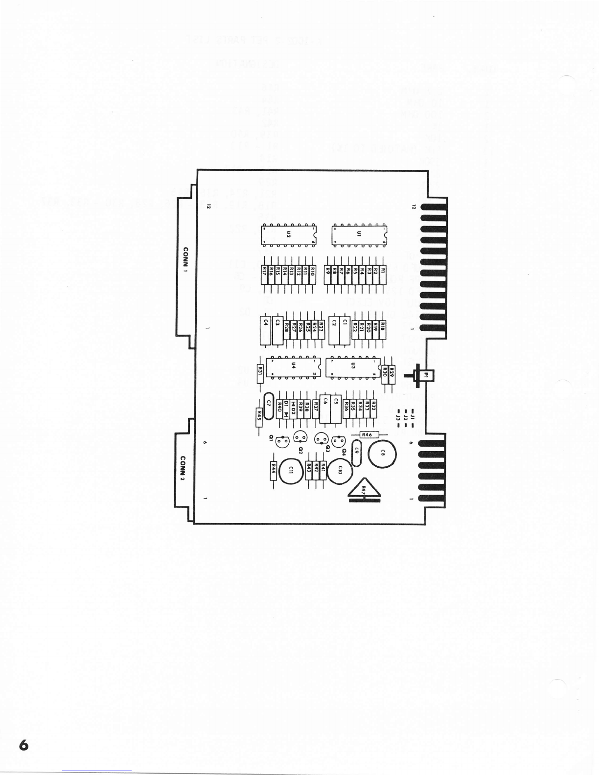
MTU K-1002-2 User manual

l|ioro
Teehnology
IInHmlted
K-1
002-2
8 Blr AUDIO
DIGITAL
TOANALOG
CONVERTER
FORCOMMODORE
PET.2OO1
HARDWARE
MANUAL
JULY
1979

coHrRIGlrT
rrcnrcE
197.9
This manual is crcpyrighted. Ttris includes the verbal description, PC artworK,
diagnostic programsi, cgnraLional prograns, and specification sheets. The custqner
rnay
make machine readable copies of the software routines for use only oT
corqr.rters cr'med directly by him or his scmpany. lftrey nay not be reproduced for
use with systems sold or rented.
Micro Techrnlogy Unlimited
841 Galaxy Way
POBox 4595
llanchester, NlI 03108

K.1002.2
UNPACKINGANDINSTALLATION
TheK-1002-2
8 Bit AudioSystem
for the PET
is a carefu'l'ly
engineered,
manufactured,
and
tested
product
that shouldoperate
perfectly whenhandled
and
installed accord'ingto the following instructions. SinceCMOSintegrated
circuits
are usedon the board, damagefrom
static discharge
is possjble. When
handling
the board,
always
pick it up
by
the output
jack whichis connectedto ground.
Before
plugging
it jnto or removing
it fromthe PET,
discharge
yourself to the PET
case
first.
Installation is quite simple,
merely
plug
the unjt onto
the user
port and
secondcassette
port of the PET. If other accessories
or a second
cassette
unit
are
to be
used,
p'lug
theseonto the edge
fingers of the K-1002-2.
Ourunit does
not load any
of the user
port signals
signifjcantly because
of the CMOSlogic
ut
jl ized. Any4, 8, or 16
ohm
speaker
maybe
p'lugged
into the RCA
phono
jack at
the rear of the board. Alternat'ive1y
an
aud'iocable
may
be
p'lugged
in andan
external anplifjer used
for more
volumesuchas at a club
meetjng
or show.
If the K-1002-2MusjcSoftware
package
has
been
purchased,
follow the
instructions includedwjth the cassette
to verify that the boardis working.
0therwise
enter the following
BASIC
program
andRUNit:
A=0:B=255:
C=59459
POKE
C,A:POKEC,B:G0T020
Theresulting soundshould
resemblethat of a
misfiring race car. Thevolure
control on the boardshouldhavea rangefrom
complete
s'ilence
to slightly above
the point of distortion.
Notethat the CB2s'igna1
from the 6522
UIA
is also connected
'into
the audjo
anpl
if ier circu'itry. Theref
ore any
game
programs
or simple
music
programs
that
use
thjs signal to generate
soundwill still be usablewith the K-1002-2. Oneof
these
prograns
could
also
be
usedto checkout the board.
This
completescheckoutof the I Bit AudjoSystem. If any
problsns
are
experienced,
see
the sectjon
on
troubleshootjng
beforereturning
the board
to the
factory.
10
20

SP
ECIF
ICATIONS
Phys'ica'lSjze: 5 incheswide
by 4 inchesdeepoverall by 1.13 inches
thick
Connections:
I 24
p'in
edge
connector,I 12
pin edgeconnector,1 set of 24
edge
fingers, andone
set of 12edge
f ingers. All s'ignalsare
fed through
frqn the edgeconnectorsto the corresponding
edge
fingers.
DACsection:
B bits, offset binary
encoded,
typ'ica11/4 LSBlinearity, guarenteed
monoton'ic,5 vol
t swi
ng, 6.25Koutput
impedance,5 vol
t supply
'is
filtered andusedas the
referencevoltage.
Fil ter section:
6 po1es,
0.5dBChebyshev
response,
cutoff f
requency
'is 3.5kHz.
Po,ver
anp
sect
j
on: power
output: 150MW
jnto 1.6ohms,
300MW
into 8 olms, 500fvlW
'into
4 ohms. Amp'l
if jer response
is flat wjthin 3dBfrqn 30to ZAkHz
wjth an
8 ohm
load. Distortjon at full power
output
into B
ohms
at lkHz
is less than &.
Porverrequ'irements:
Single
+5
volt supply. Ripple andnoisewithin the aud'io
rangeshouldbe
less than
2S4V.
PoverConsumption:
Quiescent
current
drain is less than 50MA.Worst
case
drain at
f
ul
I power,
4 ohr I
oad, an
d squarewaveoutput i s 30ft1A.
Signal
loading:Less
than L0uA
and
10pFload'ingon
the 8 b'inaryinputs. CBz
input
is loaded
by
240<
to ground.
PIN CONNEgTIONS
(
i ndustrystandardnumbering)
SIGNAL
CONNEffM
1
2
3
4
5
6
7
8
9
t0
11
I2
SIGNAL
F.T
.
F.T.
F.T
.
F.T
.
F.T
.
F.T.
F.T
.
F.T.
F.T
.
F.T.
GROI,FID
GROLT{D
SIS'IAL CONNETTOR SIS{AL
F.T.
F.T
.
DATABIT O
DATABIT 1
DATABIT 2
DATABIT 3
DATABIT 4
DATAB
IT 5
DATA
B
IT 6
DATAB
IT 7
cB2
F.T.
GR,OUN
D
+5 VOLTS
F
.T.
F
.T.
F.T.
F.T.
A
B
D
E
F
H
J
K
L
M
N
CONNE
ffOR
A
B
c
D
E
F
POWER
CONNECTOR
*** F.T.
*** N.C
.
S
IGNAL POWER
N.C.
N.C
.
N.C
.
N.C
.
N.C
.
N.C
.
1
I
2
3
4
5
6
2FeedThroughto correspondi
ngedge
f ingers,
no on-boardconnect'ion
Noconnection
to edge
fingers or anythingelse

PRINCIPLES
OFOPERATION
The
K-I002-Z
I Bit Aud'io
System
consists
of three dist'inct sections. The
8
bjt digital-to-analog
converter
(DAC)
acceptsan 8 b'it b'inaryinput from the user
port on
the PET
and
produces
a DCvoltage
d'irectly
proportional
to the unsigned
binary valueof the input. The
6-po1elowpassfilter blocks
all sanpling
di
stortion frequencjes
above
approx'imate'ly
3.5kHz. Thi
s f il ter j
s necessary
f
or
cleansounding
musicfrom the DAC. Theaudio
power
anp'lifier boosts
the filter
output signa'l
to the level required
for drjv'inga speaker. The
CB2
pin on
the PET
user
port is also tied'into the anplifier circuitry. A volume
control determines
the gain
of the amplifjer and
thus
the volumeof the soundreproduced'inthe
speaker. In order for the boardto operatesolely from
a s'ing1e5 volt power
supply,
several
jnnovative
circujt techn'iques
have
beenincorporated.
Lookingat the DAC
sectjon
first (1eft portjon
of the schematic
draw'ing),
it
is seen
that the weighted
resjstor methodof conversionis used. The
Clv1OS
buffers
in Ul and
U2make
very
good
analog
switches
whichswitchthejr outputsbetween
exactly
lfound
and
exactly
the supp'lyvoltage
(+5
volts) jn responseto the input
s'igna1.
The
only error in thjs switchingact'ion
is a f inite output impedanceof
approximatel
y 200ohms. Ctvl0Sbuff
ers, rather
than
i nverters, are usedbecause
the
two stagesof "gain" internally assurescompleteswitchingof the output
even
jf
the input swingsless than 5 volts. TheDACnetwork
produces
an output vo'ltage
d'irectly wi
th a source
impedance
of approximately
6.25K. tl'ith
al
I zeroes
input,
the output is zero
volts; with all ones
input, the output
is 5 volts. Loading
the
output
hasno
effect on
ljnearity but it will reducethe s'igna'lswing.
In order to insure
accurate,monotonic
performance
of the DAC,the most
si
gn'if
jcant bit js actually
f
our ClvlOS
gates
and
four 51Kres'istors in parallel
whjle
the next mostsign'ificant b'it is two in paralle'I. Theremain'ing
b'its are
single gates
sjnce
the ratio of the wejghtingresjstors to the gate
output
'impedance
is large
enough
to ignore. By
using
para'l'lel
andseries combinations
of
51K
resistors for the most
sjgnificant 5 bits, jt'is possible
to use
relatively
jnaccurate
res'istors
in the DAC
andstill achieve
1/4 LSBlinearity wh'ich
js about
.4. This'is dueto statistjcal averag'ing
among
the resistors, particularly the
critical most
significant b'it. Even
so, factory assembledunits have
hadthe 51K
resjstors matchedto w'ithin 1%. Althoughthe
morecommon
R-ZR
res'istor
ladder
networkcould have
been
used,moreresjstors wouldhavebeen
requiredto get the
sane
degnee
of statist'ical match'ing.
An integrated
circuit DAC
was
not practical
sjnce
all that are currently ava'ilablerequire a negative
supplyvoltage
for
either the DAC
itself or for a current-to-voltage
converter
operational
anplifier.
Note
that the 5 volt power
supp'ly
is fjltered andusedas a reference
for the DAC.
Wh'ilesmall anounts
of noise
are
fi'ltered out, 60Hzripp'le on
the 5 volt supply
is
I
jkely to result in hum
from the speaker.
Thefilter c'ircu'it is wherethings start getting
unconventional.
Thef ilter
actually consists of three.two-po1e
stagesconnected
'in
cascade.
Eachsection
js
a resonantlowpassfilter, 'i.e., the response
curve
may
peak
somewhat
just before
cutoff. t^lith
proper
selection of sectioncutoff frequencies and
Q
f
actors
(peaking),
a very nearly
flat passband
andsharp
cutoff is obtained. Passband
ri pple
'is less than .5dBand
the cutoff slope
is such
that 30dBattenuat
jon 'is
obta'ined
at just 1.35tjmes the cutoff frequencyof 3.5kHz. Note
that the 5
volt
sw'ingof the
DAC
'is
reduced
to about
2,5 volts through
the filter by virtue of the
22W,'input
resistor to the f irst fjlter stage.
Eachfilter sectjon'is implsnentedas a biquadratic
fjlter which
consjsts
of
an invertjng surnmingamplif
jern d leaky inteE"fEEb7i-ffi?an ideal integrator all
connected'ina 1oop. Althoughthree operationalanplifiers are
required
for the
ci
rcu'it, 'its advantagesare
many. In parti
cular, hi
gh
Q
f
actors are
possi
bl
e wi
th
modest
anpf
ifier gain. In addjtion, sensjtivity of the responsecurve
to
componenttolerance'is very
1ol. These
characteristicsallol the useof linearly
bjased
Cl{S
gates
as
jnverting
operationalanpf
if iers. Perf
ormance
of the f ilter
using
the CtflS
gates
'is
indist'inguishablefrom the performance
using
true op-anps
such
as
the 741. See
the NationalSemiconductor
CISS
data
bookfor more
jnformation
on
linear CIOSapplicat'ions. 3

. Ihg audio
power
arpliflef is-a spegia]
high
efficiency desigrr
that allo,'ls
a
significant power
output
with only a single 5 vo'lt power
supply-and
no output
transf
ormer. Three
para'l1e'l
connected
CiOS
gatesprovide
most
of the voltage
anplification in the circujt as
well as
presenting
a high input impedance
and
havinga moderately1or
output
impedance.
The
output
stageis fully comp'lenentary
and
incorporates
considerablelocal feedback
of its orn. The
voltage
gain
of the
outptt stageis approximately
18. 0verall feedback
from the output backto the
vo'ltageanplifier input comp'letes
the loop
and
gives
a closed
loop
gain
of about
3.5
with maximum
volume.
The92P1,01
(NPN)
and92PU51.
(Pl'lP)
output
transistors
actually contain a one-anpcapability transjstor chip
in a
modified
T0-92
plast'ic
case. Thjs is ttp sanechip as usedin the Motorola
MPSttrLand
MPStlSl
plast'ic
power
transistors. Wjthan 8 ohn
'load,
the anp'l
if ier outprt can
swing
to within
.3 volts of the 5
volt supplyor gnound
before
saturating. The
2.7
otm
resistor
and
.luF capacitor
(R46
andC9) accross
the outpt preventposs'ible
osci'llation
w'ith'induct'ive'loads.
R39,R40,01, and
D2form
a bjas network
wh'ichallols a
couple
of mjlliamps
to flol in the output trans'istorsat all times
to minimize
class-B
crossoverdistortion. R45
mixesthe CB2
s'igna1
fromthe connector
in with
the
filtered DAC
output
to allor continued
useof this s'igrra1with existing game
andsimple
music
prograns.
TROUB
LESHOOT
ING
D'iagnosing
problems
with the K-1002-2board
is fairly simp'lebecause
of the
un'id'irectional
s'igna1
flor and
minimal
interaction anongcircujt components.
If
the boardis completely'inoperative,first do a thorough
visual inspect'ion
of the
board. Lookon the sol
der si de of the boardfor component
I
eadsthat maybe bent
and
shorting out to adjacent
pads
or PC
runs. Checkfor loose
components
andthe
possj
bi1ity of a col
d sol
der
joi nt.
If careful inspectionfails to turn up anything,
enter and
run
the prognam
given
earl
ir. Then
usinga scopeor anpl
if ien/speaker
if a scope
is unavajl
ab]e,
find out where
the sigal is beinglost. Thefirst point to check
is the node
whereall of the DACresistors are
tied together. Thesignralshouldbe
a square
wave
modulatedat a 60Hzrate (ca'used
by
timr interrupts in the PET)
with ground
and
+5
voltage
levels. Next
check
the output of the first filter sectionwhich'is
U3-8. The
waveformshould
be
sorneylhatroundedwjth voltage
levels of about
L.25
and
3.75volts. The
next stageoutput
(U3{) should
be
ssns{hatless rounded
w'ith
a hint of ringing on
the squarewave
edges. Againthe signa'l
levels (1ess
ringing) should
be 1.25
snd 3.75volts. The
'last
stageoutput
(U4-6)
has
cons'iderable
ringing at a little over 3kHzbut still the sane
voltagelevels. If
the sigrtal js lost anylhere
jn the fjlter or the voltage
levels are
cons'iderably
offset (greater
than
.5 volt deviat'ion)
from thejr proper
valrcs first wiggle
all
associated components
to see
'if anythi
ng
changes. If thi
s f
a'i1s,the associ
ated
CD4069
(the 74C04
is an equivalent)should
be
replaced. Be
sure to usea CD4069
or a 7464; other varieties oF invertersmay
not be
suitable
f
or I
inear operation
or mayhavetoo h'igh
an
internal impedance.
If the problsn
is in the power
amp'l
'if
ier, first measurethe output
trans'istor
collector voltage
(tfte
little tabs
sticking out the top of the transistors are the
collectors)w'ith no sigrra'|. This voltage
should
be
within a quarter
volt of 2.5
volts. If it is off consjderably,oneof the 4 transistors in the output
stage
maybe shorted or openor the CttOSvoltage anpl
if ier maybe bad. Temporarily
cut
the l
jne running
from
U4€, 10, and
12to the junction of Dl and
D2
andmeasure
the col
I
ector voltage again. If it i
s now
centered,the CI'OSis bad;
otherw'ise
one
or moretransistors are
bad
or oneof the biming resistors (R38-R43)
'is open.
The
anplifier is only partially protected
fnomoutoutshorts so exercisecare
in
connecting
the speaker
and
don't run the unit with the volune
full up
whenthere
'is an obvious
probl
sn suchas a speakerl'ine short.
If the custoner
is unableto f ind the prob'lan,
return
the un'it to the factory
f
or servicing
a'longw'ith a descriptionof the malfunct'ion.
This is a
rel
at'ive1y
simple
boardand
factory repair canusually
be
accomplished
in a coupleof days.
4

qJAN.
1
1
2
1
2
t3
I
3
1
4
L2
1
2
L
1
2
6
2
1
2
1
1
1
1
2
2
I
1
t
1
PART
2.7 ff'tti
10 c}tM
100 fir{
1K
10K
51K
(MATfiED
T0
390K
820(
22W.
24U,
1Ofr
180K
13(X
680K
I.M
POT
220t.FD 6V ELEgt
47OPF
PO.Y
CAP
.lUFD
L?UZsU
1000r,F
10vELEcr
11,14148DIOIES
Ptu222
Pr{2S7
92
Pml
92
PU51
cD4050
cD4069
PHONOPLUG
PC
BOARD
CONNPC SINGLE
6
CONN
PC
DUAL
1.2
K-1002.2
PET
PARTS
LIST
DES
IGI{ATION
R46
R44
R41,R43
R42
R39,
R40
11) Rl - R13
Rt4
R15
- R17
R29
R21,
R34,R36,R45
R18,
R19,R23
- R26,
R28,R30
- R33,R37
R35
R20,R22
R27
R47
c1o,c1l
cl-c6
c7;ce
c8
01,D2
q2
Q1
Q3
Q4
ul, u2
u3,u4
.156SP
.156SP
5

nffiffiffi
[*'-] f-=-l
ffiffi
f-:"1
[Hffi
3ffiffi,ffi
i*,.,?Rr1b
Hoffi%
6

Rr9
tooK
t@K
R3+
z40K
R20
rhx
I
lhri
'3rDsr>Or2
lr/z
r
5lK
R3
5lK
I
h\
.,V
f--.F>
I t'/'
l--,1h.>
cw,t- L I Lt'
-----t-,,h>
W
+
-,lh>'
,ror*,
^ f, (
| ,|ib,
L"'
oco'Nt-r ,.S
coNNt-lt D'.-
o-'V
coNNt-F |u}\
o-'V'
COMN I, E
o-ll
oArA
ts,r
r S9!!l-tF"
t-.-
co&^ll-C luz\
-Jl@€1>'o WI
,-L
couil/ -n
ct
47OPF
R4
5tK
Rlt
5rK
Rra Rl3
stK slK
Rrl Rt6
azoK azo(
DATA 8 /f 7
pATt B/T 4
D/rt 8/T 5
2^T/l 8/7 |
2/T/4 B /T 3
DATA I /T 2
rloK
'F
f/tfFR ouT
+
| r ,lUO/o
R46
2.7 JL
l2v.
RAW DAC OUT
R44
lo4
DA.A a/7 95
c82 S/6MAt
crl
2?Orf
Rtz
R5
Rrg
RZ1
R23
loo^
t2
caNN/- //. /2
coNtu2- A
/Y[80 T
TC
HNOI06
Y U
NL
I
11IT
E
D
K-ICA2.Z
8
B/T
DAC
rOR PfT

Table of contents