CONTENTS
1.
2.
bd
VW.
GOTOF
AD
ss
5.06%,
aie
Shales
cele
race saya
laeyiat
bumps:
by
inca
BoB
acate
Kekied
Gea
yare
Javaliphere
©
elepdl
Guacatte
@ists
Sawicwteee
2
Wo 1,
Control
Functions
........
2
Va.
:2,
Voltage
Selector..........
3
1,
3.
Functions
..........-.-5
3
1.
4,
How
To
Read
Signals
5
1.°¢5.
Semiconductor
Switch
5
Removal
Procedures
..
1.2200.
eee
ee
cee
reer
cece
eee
eee
ee
eee
tee
tent
eee
e
renee
6
2.
12
Top
Cover
Ass’y,
Bottom
Cover
Ass’y
and
Synthesis
Mechanism
Ass’y
with
Power
Supply
Ass’y...
6
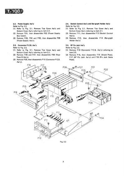
2.
2.
Power
SUPPIV
ASS
Vi?
5.22850
hissed
LORS
hs
ad
tate
See
teig
oe
Wit
eset
Ss
ent
Eee
Bee
Be
dk
ede
7
2
3.
Connector
P.C.B.
Ass’y
«0.
ee
ee
eee
eee
7
2.
4.
Switch
Control
Ass’y
and
Bar-graph
Holder
Ass’y
. .
7
2.
5.
GP
Pin
Jack
Ass’y
2...
eee
cee
eee
7
2
6.
Switch
P.C.B.
Ass’y
and
Votume
P.C.B.
Ass'y
2...
cee
cee
ee
ete
eee
en
neee
8
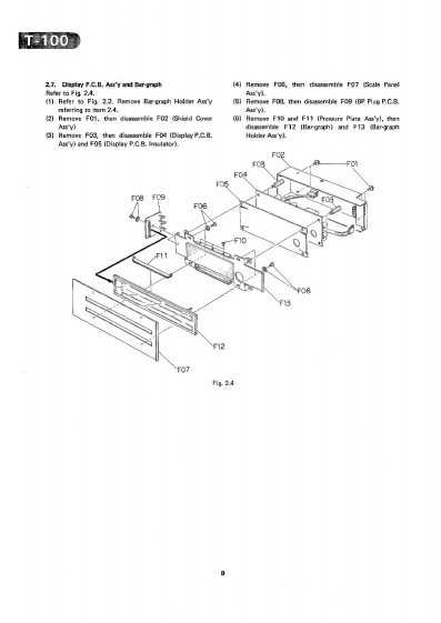
2
7.
Display
P.C.B.
Ass’y
and
Bar-graph
2...
ce
cee
eee
ett
eee
et
neee
9
2
8,
Power
Supply
P.C.B.
Ass‘y
and
Power
Transformer
.
10
2
9.
Rear
Panel
A
Ass'y,
Power
Switch
and
AC
Inlet...
10
Measurement
Instruments
..
20...
0000
v
eee eee
e
renee
10
Parts
Location
for
Electrical
Adjustment...............
11
44,
CUrrent
TY
Pe
accede
ee
See
eee
ee
ea
1
4.
2,
Previous
Type
........
2.
eee eee
eee
eens
11
Adjustment
and
Measurement
Instructions
..........-..,0000-
staat
12
5.
1.
Current
Type.............08
See
ODE
ae
tein
&
foe
Sab
Sande
diby
skater
ere
iececaueuhw
sara
rapsress
abate
cates
12
5,
2,
Previous
Type»...
eee
ee
eee
eee
eee
15
Mounting
Diagrams,
Circuit
Diagrams
and
Parts
List
18
6.
1
IC
Block
Diagrams
18
6
2
Connector
P.C.B.
Ass’y
19
6
3.
Power
Supply
P.C.B.
Ass’y
21
6
4,
Wow
&
Flutter
P.C.B.
Ass’y
..
23
6,
5,
Switch
P.CB.Ass’y..
ce
eee
cette
ee
ete
nent
cette
emcee
tense
tee
tn
nee
25
6.
6
Oscillator
'P.C:B.:Ass’yoss.i.3
eccd
ioe
de
ey
eee
bie
ea
ene
eee
ee
ne
25
6.
7.
Absolute
Rectifier
P.C.B.
Ass’y
..
2.22.20
0.05
:
esa
eh
6.
8
Linear/Log.
Converter
P.C.B.
Ass’y
Bila
ghd
29
6
9.
Distortion
P.C.B.
Ass’y
1...
eee
eee
eee
Setiexionpe:
2Ot
B20Os”
“Noltitne
PiC.B
Ass!
y
se
asscz-es
seis
as ee
setcatee
ceraeetarsactes
Sie
re
eran
el
natin
Zoe
Se
halon
Se
nl
tne
Se ed
“awd
arated
33
6.
11.
IHF-A
WTD
Network
P.C.B.
Assy
35
€
12.
Display
P.C.B,
Ass’y
37
6
13.
Analog
Multiplier
P.C.B.
Ass’y
39
Mechanism
Ass’y
and
Parts
List...
2.2...
0.
cece
eee
eee
ee
eee
eee
41
as
OV
SV
MUESIS
A350
cea
wand
rated
cas
int
Diese
ei
Mees
ne
ar
eles
slsdeeted
hap
aoe
aces
Bb
anata
Nay
Mian
ore
Sara
Macavauehas
anlar
raneea
41
7. 2.
Synthesis
Mechanism
Ass’'y
{(AO1)
2...
ce
ce
eee
eee
eee
nee
eee
42
7
3.
Power
Supply
Ass‘y
(A02)
43
7
4.
Switch
Control
Ass’y
(B01)
45
7
5.
Bar-graph
Holder:Ass’y:
(BOQ)?
seg
2-5,
e-v
ecesce
womeeees
dasha
veteraereeraye
re
wos
oe
tebe
validy
dae
Ae
46
7.
6.
Connector
Ass’y
(B03)
47
Block
Diagram
.......,
48
Wiring
Diagram
........
49
Troubleshooting:
ca
teen
he
ie
a
eye
eee
ee
Baik
ea
ce
aresw
ddd
eased
da
febalra
te
1a
Ja
Ranaehareialayalniinadereoe
end
ae
lo
50
10.
1.
Notes
50
10.
2.
Troubleshooting
.
50
Specifications
53