Newport Electronics P6000A User manual

P6000A/P5000
OUTPUT OPTIONS
ISOLATED PARALLEL BCD
DUAL 8 A RELAY
ISOLATED ANALOG OUTPUT
11361ML-01
NOTE: Refer to 10627ML-XX for P6000 Output Options Manual.
© Copyright 1995, NEWPORT ELECTRONICS, INC. ALL RIGHTS RESERVED.
This documentation may not be copied, photocopied, reproduced, translated, or
reduced to any electronic medium or machine-readable form, in whole or in part,
without prior written consent of NEWPORT ELECTRONICS, INC.


i
TABLE OF CONTENTS
ISOLATED PARALLEL BCD OPTION PAGE
1.0 GENERAL INFORMATION ..............................................................................1
2.0 MECHANICAL INSTALLATION.........................................................................1
3.0 ELECTRICAL CONNECTIONS .........................................................................1
3.1 Power ................................................................................................1
3.2 BCD Outputs ...........................................................................................2
3.3 Polarity Output.........................................................................................4
3.4 Decimal Point Binary Address...................................................................4
3.5 Overflow Output........................................................................................4
3.6 Alarm Outputs .........................................................................................5
3.7 DATA READY Output...............................................................................5
3.8 Instrument Select Inputs ...........................................................................5
3.9 HOLD Input .............................................................................................5
4.0 JUMPER SELECTION.....................................................................................6
5.0 CONTROLLER INTERCONNECTIONS..............................................................7
5.1 Interconnections with a Parallel BCD Printer ...............................................7
5.2 Interface with Programmable Controllers.....................................................9
6.0 PARALLEL BCD DRAWINGS........................................................................ 10
ILLUSTRATIONS
Figure 5-1 Connections with a Parallel BCD Printer
Using Right-hand Decimal Point ..................................................7
Figure 5-2 Connections with a Parallel BCD Printer
Using Left-hand Decimal Point.....................................................8
Figure 6-1 Parallel BCD Board Assembly Diagram...................................... 10
Figure 6-2 Parallel BCD Board Schematic Diagram..................................... 11
Table 3-1 Required Address to Enable Outputs ...........................................3
Table 3-2 Decimal Point Binary Address.....................................................4
CHG ECO NO DATE BY CHK
B 9261 21 JAN 98 ML

ii
DUAL 8 A RELAY OPTION PAGE
1.0 GENERAL INFORMATION .............................................................................. 12
2.0 MECHANICAL INSTALLATION......................................................................... 12
3.0 ELECTRICAL CONNECTIONS AND JUMPER SELECTION ................................ 12
3.1 Relay Outputs.......................................................................................... 12
3.2 S3 of the Relay Board............................................................................... 13
4.0 RELAY BOARD DRAWINGS........................................................................... 14
ILLUSTRATIONS
Figure 3-1 TB4 Connector with Electrical Connections................................... 12
Figure 3-2 Relay Board Pin Groups ............................................................. 13
Figure 4-1 Relay Board Assembly Diagram .................................................. 14
Figure 4-2 Relay Board Schematic Diagram ................................................. 15

iii
ISOLATED ANALOG OUTPUT OPTION PAGE
1.0 GENERAL INFORMATION .............................................................................. 16
2.0 SPECIFICATIONS .......................................................................................... 16
2.1 Power and Signals ................................................................................... 16
2.2 Environment............................................................................................. 16
2.3 Output Control ......................................................................................... 16
3.0 ELECTRICAL CONNECTIONS & ADJUSTMENT LOCATIONS ............................ 17
4.0 CONFIGURATION PROCEDURE ..................................................................... 17
4.1 Output Range Selection............................................................................ 18
4.2 Display Range Selection........................................................................... 18
4.3 Span Range Selection .............................................................................. 18
4.4 Offset Range Selection ............................................................................. 19
5.0 MECHANICAL INSTALLATION......................................................................... 20
6.0 FRONT PANEL SETUP................................................................................... 20
7.0 CALIBRATION................................................................................................ 21
7.1 Voltage Output (V01)................................................................................ 21
7.2 Current Output (I01, I02)............................................................................ 21
7.3 Current Output (I02).................................................................................. 22
7.4 Preamp Zero Adjust (R7)........................................................................... 23
8.0 ISOLATED ANALOG OUTPUT DRAWINGS ...................................................... 24
ILLUSTRATIONS
Figure 3-1 Isolated Analog Output Option Rear View ..................................... 17
Figure 8-1 Isolated Analog Output Assembly Diagram................................... 24
Figure 8-2 Isolated Analog Output Schematic Diagram.................................. 25
Table 4-1 Output Ranges........................................................................... 18
Table 4-2 Display Ranges.......................................................................... 18
Table 4-3 Span Ranges............................................................................. 19
Table 4-4 Offset Ranges............................................................................ 20

iv

1
ISOLATED PARALLEL BCD OPTION
1.0 GENERAL INFORMATION
The optional parallel BCD board works concurrently in two output modes: 6-digit
parallel BCD (24 lines) and addressable 3-digit. In addition to the 6-digit BCD, this
board outputs the alarm condition (High, Low and Go), polarity, overflow, and
decimal point binary address signals. The outputs are three-state and electrically
isolated from the main board. They are active when the appropriate address is
applied on connector P4, pins L24, U24, L23, and U23. The inputs are internally
connected to the main board via the interconnection of P5 with J5.
Outputs are available on P4, a 50-pin dual-row header at the rear of the board. The
P4 mates with a standard, 50-pin mass-terminated connector. The P4 outputs can
be frozen by making the HOLD input (P4-U21) low. Although the BCD outputs are
always valid, the DATA READY signal goes active low for approximately 0.2
millisecond when BCD data is updated.
2.0 MECHANICAL INSTALLATION
The parallel BCD board is positioned as an upper board in the P6000A/P5000.
Refer to the exploded view in the main board manual.
To avoid electrical shock be sure to disconnect the unit from its power supply.
To install:
1. Hold the board upside-down with components facing the main board.
2. Position the P5 pins to mate with the J5 connector on the power supply
board.
3. Push the board downward until it rests on the upper rear panel and the
display board.
3.0 ELECTRICAL CONNECTIONS
NOTE: The software switch SS3 of Configuration 2 must be set (XXX1XX)
to activate the parallel BCD board. For more information, refer to
Section 4.1 of the P6000A/P5000 main board manual.
3.1 POWER
A n is olat ed + 5 V ±10% ext ernal power supply is required and s hould be c onnect ed t o pi n
P4-L21 (+5 V) and pin P4-L19 (ISO GND). If isolation is not required, S5A, S5B, S6A, and
S6B may be installed to power the parallel BCD option by the main board.

2
3.2 BCD OUTPUTS
The board is factory-set as 6-digit parallel BCD. Outputs are enabled when the
binary address on the instrument select lines, pins L24, U24, L23, and U23, match
the board address (set by pin group S1). The output polarity is normally positive
true (reversible by S4) and each output can drive 10 LSTTL loads.
(N/C) ALARM LOW L1 U1 ALARM HIGH (N/C)
(N/C) N/C 2 2 ALARM GO (N/C)
(N/C) N/C 3 3 N/C (N/C)
(N/C) N/C 4 4 N/C (N/C)
(N/C) BCD 400 k 5 5 BCD 800 k (N/C)
(N/C) BCD 100 k 6 6 BCD 200 k (N/C)
(ISO GND) ISO GND 7 7 N/C (N/C)
(N/C) BCD 40 k 8 8 BCD 80 k (N/C)
(N/C) BCD 10 k 9 9 BCD 20 k (N/C)
(N/C) BCD 4 k 10 10 BCD 8 k (N/C)
(N/C) BCD 1 k 11 11 BCD 2 k (N/C)
(ALARM HIGH) D P 2 12 12 D P 4 (ALARM LOW)
(BCD 400 k) BCD 400 13 13 BCD 800 (BCD 800 k)
(BCD 100 k) BCD 100 14 14 BCD 200 (BCD 200 k)
(BCD 40 k) BCD 40 15 15 BCD 80 (BCD 80 k)
(BCD 10 k) BCD 10 16 16 BCD 20 (BCD 20 k)
(BCD 4 k) BCD 4 17 17 BCD 8 (BCD 8 k)
(BCD 1 k) BCD 1 18 18 BCD 2 (BCD 2 k)
(ISO GND) ISO GND 19 19 D P 1 (OVERFLOW)
(DATA READY) DATA READY 20 20 POLARITY (ALARM GO)
*ISO V+, 4 5 TO 5 5 V 21 21 *HOLD (HOLD)
(N/C) N/C 22 2 2 OVERFLOW (N/C)
*BOARD ADDR B4 23 23 *BOARD ADDR B8
*(BCD 1-800 ENABLE) BD ADDR B1 24 24 *BD ADDR B2(BCD 1-800k ENABLE)
(N/C) N/C L25 U25 N/C (N/C)
( ) Output in addressable 3-digit-at-a-time mode
* An input
N/C No internal connection

3
To enable the outputs, install jumpers on the pin groups and apply the proper address
on the instrument select lines as indicated below:
6-Digit
Parallel BCD S1 Positions Connector P4 with
Instrument Select Lines
U23 L23 U24 L24
Install jumpers on B8, B4, B2, B1* 0000
S2-A and S3-A; U5A B8, B4, B2, B1 0001
and U6A on XU5A B8, B4, B2, B1 0010
and XU6A sockets. B8, B4, B2, B1 0011
B8, B4, B2, B1 0100
B8, B4, B2, B1 0101
B8, B4, B2, B1 0110
B8, B4, B2, B1 0111
B8, B4, B2, B1 1000
B8, B4, B2, B1 1001
B8, B4, B2, B1 1010
B8, B4, B2, B1 1011
B8, B4, B2, B1 1100
B8, B4, B2, B1 1101
B8, B4, B2, B1 1110
B8, B4, B2, B1 1111
Addressable 3-Digit
Parallel BCD S1 Positions Connector P4 with
Instrument Select Lines
U23 L23 U24 L24
ENABLES ENABLES
BCD 1 - 800 BCD 1k - 800k
OVRFLW, HI,LO,GO D.P. 1,2,4, POL
Install a jumper on
S2-B and S3-B. X, X, B2, B1 X, X, X, 0 X, X, 0, 1
U5A and U6A on X, X, B2, B1 X, X, X, 1 X, X, 0, 0
XU5B and XU6B X, X, B2, B1 X, X, X, 0 X, X, 1, 1
sockets. X, X, B2, B1 X, X, X, 1 X, X, 1, 0
0 = Open or TTL High level (more than 2.0 V) X = Don't Care
1 = Ground or TTL Low level (less than .8 V) * = Default Setting
Table 3-1 Required Address to Enable Outputs

4
3.3 POLARITY OUTPUT
This three-state output is active when Digits 1, 2 and 3 are enabled. Signal
polarity can be reversed by a push-on jumper at S4. With a jumper on S4-A, a
high level corresponds to a positive display value.
3.4 DECIMAL POINT BINARY ADDRESS (D.P. 1, 2 AND 4)
These three-state outputs are enabled with Digits 1, 2 and 3. Signal polarity can be
reversed by a push-on jumper at S4. With a jumper on S4-A, the outputs represent
positive true binary address of a right-hand decimal point (see Table 3-2).
Decimal Point Position D.P. 4 D.P. 2 D.P. 1
FFFFFF. 001
FFFFF.F 0 1 0
FFFF.FF 0 1 1
FFF.FFF 1 0 0
FF.FFFF 1 0 1
F.FFFFF 1 1 0
Table 3-2 Decimal Point Binary Address
3.5 OVERFLOW OUTPUT
This three-state output is active when Digits 4, 5 and 6 are enabled. S4 reverses
the polarity. When a jumper is installed on S4-A, an overflow condition makes this
output go high. In this case, all of the digits of the parallel BCD board
represent a "9" (BCD 1001). The decimal point address corresponds to the
point selected as Fixed Range decimal point. S7 connects this output to
pin U22 of the P4 connector.

5
3.6 ALARM OUTPUTS (HI, LO, GO)
These three-state outputs are enabled with Digits 4, 5 and 6. S8, S9, and S10
connect HI, LO, and GO to P4-U1, L1 and U2, respectively. The polarity is positive
true (high level corresponds to an alarm condition) when a jumper is installed on
S4-A.
3.7 DATA READY OUTPUT
The output is always valid because the parallel BCD data updates synchronously
with a single clock pulse. A negative true DATA READY signal goes high,
however, for about 0.2 milliseconds when the parallel BCD data is updated.
3.8 INSTRUMENT SELECT INPUTS (P4-U23, L23, U24 AND L24)
These are TTL-compatible inputs with 47 k Ohms pull-up resistors. When the input
logic levels match the instrument address (set by S1), the outputs are enabled.
When the logic levels do not match, they are in high impedance. Refer to Table 3-1.
3.9 HOLD INPUT
When low, this input freezes the outputs and makes the DATA READY low true.
The internal BCD data continues to update. The updated data replaces the
outputs when HOLD goes high.*
* If the HOLD input goes high during transmission, the output update is postponed in
order to prevent erroneous output. Each transmission requires approximately 10
milliseconds.

6
4.0 JUMPER SELECTION
Pin Group Function
S1 Selects the binary address (Table 3-1).
S2 Jumper installed on A:* Board can be selected by four
address lines on connector P4, pins L24, U24, L23 and U23.
Jumper installed on B: A high or low level on L24 selects
the board when S1-B1 or S1-B1 are installed respectively.
S3 Controls the DATA READY output.
Jumper installed on A:* DATA READY is active low when
the input address matches the board address.
Jumper installed on B: DATA READY is active when P4-L24
matches S1-B1 or P4-U24 matches S1-B2.
S4 Inverts all output logics except DATA READY. S4-A*
corresponds to positive true logic.
S5, S6 Jumpers installed on A and B of S5 and S6: The main board
powers the parallel BCD board. The outputs are not isolated
from the main board. Default setting of these jumpers is open.
S7, S8, S9, S10 Connects Overflow, High, Low and Go signals to connector
P4, pins U22, U1, L1 and U2, respectively. Default setting
of these jumpers is open.
*Default Setting.

7
5.0 CONTROLLER INTERCONNECTIONS
5.1 INTERCONNECTION WITH A PARALLEL BCD PRINTER
If printing the decimal point is not required or if the printer recognizes a positive
true binary address for the decimal point, simply connect the 24 line BCD outputs
(6 digits x 4) to the corresponding inputs of the printer. For negative true BCD and
decimal point address, install S4-B. If the parallel BCD printer accepts more than
6Êdigits, tie the unused inputs (digits 7, 8, etc.) to GND or high level, as required,
to print a BLANK on those positions.
Some printers or data acquisition systems can only accept a binary address of a
left-hand decimal point (001 corresponds to XXXXX.X instead of XXXXXX.). For
interconnection to such a system, connect each digit (4 BCD lines) to the next
more significant digit input of the printer (e.g., D1→D2, D3→D4, . . . D6→D7).
With this method, all of the digits are printed one position to the left;
therefore, the decimal point prints in the correct position. Digit 1 input and
other unused inputs of the printer should be tied to the appropriate level
to print a BLANK or zero.
P6000A/P5000 Parallel BCD Parallel BCD Printer
ISO GND L7 GND
BCD 1 L18 BCD 1
DIGIT 1 BCD 2 U18 BCD 2 DIGIT 1
BCD 4 L17 BCD 4
BCD 8 U17 BCD 8
DIGIT 2 DIGIT 2
DIGIT 3 DIGIT 3
DIGIT 4 DIGIT 4
DIGIT 5 DIGIT 5
BCD 100 k L5 BCD 100 k
DIGIT 6 BCD 200 k U5 BCD 200 k DIGIT 6
BCD 400 k L5 BCD 400 k
BCD 800 k U5 BCD 800 k
d.p. 1 U19 d.p. B1 Decimal point
d.p. 2 L12 d.p. B2 binary address
d.p. 4 U12 d.p. B4 (right-hand
decimal point)
Figure 5-1 Connections with a Parallel BCD Printer
Using Right-hand Decimal Point
1
8
P6000A/P5000 Parallel BCD Parallel BCD Printer
To appro- BCD 1
priate level BCD 2 DIGIT 1
to print BCD 4
BLANK BCD 8
BCD 1 L18 BCD 10
DIGIT 1 BCD 2 U18 BCD 20 DIGIT 2
BCD 4 L17 BCD 40
BCD 8 U17 BCD 80
BCD 10 L16 BCD 100
DIGIT 2 BCD 20 U16 BCD 200 DIGIT 3
BCD 40 L15 BCD 400
BCD 80 U15 BCD 800
BCD 100 L14 BCD 1 k
DIGIT 3 BCD 200 U14 BCD 2 k DIGIT 4
BCD 400 L13 BCD 4 k
BCD 800 U13 BCD 8 k
BCD 1 k L11 BCD 10 k
DIGIT 4 BCD 2 k U11 BCD 20 k DIGIT 5
BCD 4 k L10 BCD 40 k
BCD 8 k U10 BCD 80 k
BCD 10 k L9 BCD 100 k
DIGIT 5 BCD 20 k U9 BCD 200 k DIGIT 6
BCD 40 k L8 BCD 400 k
BCD 80 k U8 BCD 800 k
BCD 100 k L6 BCD 1 M
DIGIT 6 BCD 200 k U6 BCD 2 M DIGIT 7
BCD 400 k L5 BCD 4 M
BCD 800 k U5 BCD 8 M
d.p. 1 U19 d.p. B1 Decimal point
d.p. 2 L12 d.p. B2 binary address
d.p. 4 U12 d.p. B4 (left-hand
decimal point)
Figure 5-2 Connections with a Parallel BCD Printer
Using Left-hand Decimal Point

9
5.2 INTERFACE WITH PROGRAMMABLE CONTROLLERS
If the controller can accept 24 bits of BCD data (32 bits if other data is also
required), the 6-digit parallel BCD mode can be used.
In addressable 3-digit-at-a-time mode, only half of the I/O lines are required. In this
mode, digits 4, 5, and 6, Overflow, High, Low, and Go signals can be accessed on
the same lines of Digits 1, 2, and 3, D.P. 1, D.P.2, D.P. 4 and Polarity signals.
Parallel BCD board can be configured as an addressable 3-digit-at-a-time BCD as
follows:
1. Move U5A and U5B integrated circuits (IC) to U5B and U6B sockets.
2. Install a jumper on S2-B and S3-B.
The outputs can be enabled by an appropriate logic level on U24 and L24 pins of
P4 (see Table 3-1).
10
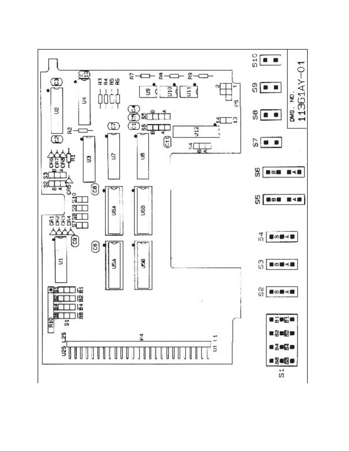
6.0 PARALLEL BCD DRAWINGS
Figure 6-1 Parallel BCD Board Assembly Diagram
11

12
DUAL 8 A RELAY OPTION
1.0 GENERAL INFORMATION
The relay option provides two Form-C relays corresponding with LO and HI
setpoints of the P6000A/P5000. The inputs are internally connected and the
outputs are available on TB4, a 6-position barrier. TB4J, a mating screw-
clamp connector, is standard.
2.0 MECHANICAL INSTALLATION
The relay board is positioned as an upper board in the P6000A/P5000. Refer
to the exploded view in the main board manual.
To avoid electrical shock be sure to disconnect the unit from its power supply.
To install:
1. Hold the relay board upside-down with components facing the main
board.
2. Position the P5 pins to mate with the J5 connector on the power supply
board.
3. Push the board downward until it rests on the upper rear panel and the
display board.
3.0 ELECTRICAL CONNECTIONS AND JUMPER SELECTION
3.1 RELAY OUTPUTS
These outputs are available on the TB4 connector (Figure 3-1). The relay
board is rated for 8 A current with resistive and 3 A with inductive loads.
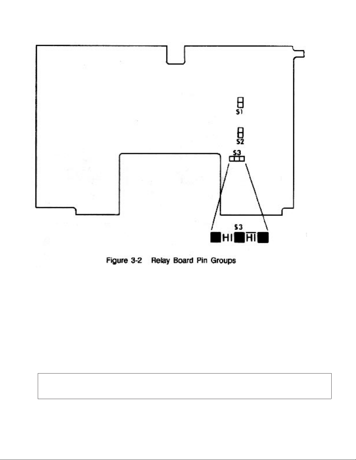
Push-on jumpers must be removed from pin groups S1 and S2 (Figure 3-2)
when the P6000A/P5000 is powered by an external battery (connected to
V+ of P2) with a voltage higher than 9 volts.
12345 6
COMMON
NORMALLY
OPEN
NORMALLY
CLOSED
COMMON
NORMALLY
OPEN
NORMALLY
CLOSED
HIGH ALARM LOW ALARM
Figure 3-1 TB4 Connector with Electrical Connections
13
3.2 S3 OF THE RELAY BOARD
If a jumper is installed on the HI position, high relay is energized when high alarm
is active.
If a jumper is installed on HI, the relay is energized when high alarm is not active
(LO or GO active). Also, with the jumper on HI, the high setpoint should be higher
than the low setpoint.
NOTE: Refer to the P6000A/P5000 main board owner's manual for low alarm
polarity reversal.

14
4.0 RELAY BOARD DRAWINGS
Figure 4-1 Relay Board Assembly Diagram
This manual suits for next models
1
Table of contents


