Newport New Focus 8712 User manual
Model 8712 Picomotor Driver
Model 8703 System Driver
User’s Manual
Single-Axis Picomotor Driver

ii Preface
EU27 DECLARATION OF CONFORMITY
Application of Council Directive(s):
☒Electromagnetic Compatibility Directive (EMCD) – 2014/30/EU
☒Low Voltage Directive (LVD) – 2014/35/EU
☒Restriction of Hazardous Substances Directive (RoHS2) – 2011/65/EU (2)
☒Restriction of Hazardous Substances Directive (RoHS3) – (EU) 2015/863 (2)
☒Waste Electrical and Electronic Equipment – Directive 2012/19/EU
Standard(s) to which conformity is declared:
☒EN 61326-1:2013 – (EMC)
☒EN 61010-1:2010 + AMD 1:2016 (Ed 3) – (Safety)
Emissions:
☒CISPR 11:2015 Industrial, Scientific and Medical Equipment Radio-Frequency Disturbance Characteristics -
Limits and Methods of Measurement
☒IEC 61000-3-2:2018 EMC/Limits for Harmonic Current Emission (1)
☒IEC 61000-3-3:2013 + AMD1:2017 EMC/Limitations of Voltage Fluctuations and Flicker in Low-Voltage
Supply Systems (1)
Immunity:
☒IEC 61000-4-2:2008 EMC/Electrostatic Discharge Immunity Test
☒IEC 61000-4-3:2006+AMD1:2007+AMD2:2010 EMC/Radiated Radio - Frequency Electromagnetic Field
Immunity Test
☒IEC 61000-4-4:2012 EMC/Electrical Fast Transient/Burst Immunity Test
☒IEC 61000-4-5:2014 + AMD 1:2017 EMC/Surge Immunity Test (1)
☒IEC 61000-4-6:2013 EMC/Conducted Disturbances induced by Radio Frequency Fields Immunity Test
☒IEC 61000-4-8:2009 EMC/Power Frequency Magnetic Field Immunity Test
☒IEC 61000-4-11:2004 + AMD 1:2017 EMC/Voltage Dips, Short Interruptions and Variations Immunity Test (1)
Manufacturer’s Name: MKS Instruments, Inc., 2 Tech Drive, Andover, MA 01810 USA
Authorized Representative’s Name & Location: MICRO-CONTROLE Spectra-Physics S.A.S., Zone
Industrielle, 45340 Beaune la Rolande, France
Equipment Type/Description: Electrical equipment for measurement, control and laboratory use
Model Number(s) (1): 8712, 8703, 8745-PS
The object of the declaration described above is in conformity with the relevant Community harmonization
legislation. MKS product conforms to the above Directive(s) and Standard(s) only when installed in accordance with
manufacturer’s specifications. This declaration has been issued under the sole responsibility of the manufacturer.
Date: 2/3/2021 Signature:
Full Name: Le Cointe Hervé
Title: Quality director
==========================================================================================================================================
1) Compliance of the above model numbers requires the use of a braided shielded cable properly terminated at both ends – if so noted in the MKS
Instruction Manual.
2) RoHS Directive has to be checked for in scope products; cannot CE mark without compliance to RoHS. RoHS Directive can be unchecked
only for systems which MKS sells which qualify for “Large Scale Industrial Tool” exclusion.

Preface iii
iii
UK Declaration of Conformity
Application of Council Directive(s):
☒Electromagnetic Compatibility Directive (EMCD) – 2014/30/EU
☒Low Voltage Directive (LVD) – 2014/35/EU
☒Restriction of Hazardous Substances Directive (RoHS2) – 2011/65/EU (2)
☒Restriction of Hazardous Substances Directive (RoHS3) – (EU) 2015/863 (2)
☒Waste Electrical and Electronic Equipment – Directive 2012/19/EU
Standard(s) to which conformity is declared:
☒BS EN 61326-1:2013 – (EMC)
☒BS EN 61010-1:2010 + AMD 1:2016 (Ed 3) – (Safety)
Emissions:
☒CISPR 11:2015 Industrial, Scientific and Medical Equipment Radio-Frequency Disturbance Characteristics -
Limits and Methods of Measurement
☒IEC 61000-3-2:2018 EMC/Limits for Harmonic Current Emission (1)
☒IEC 61000-3-3:2013 + AMD1:2017 EMC/Limitations of Voltage Fluctuations and Flicker in Low-Voltage
Supply Systems (1)
Immunity:
☒IEC 61000-4-2:2008 EMC/Electrostatic Discharge Immunity Test
☒IEC 61000-4-3:2006+AMD1:2007+AMD2:2010 EMC/Radiated Radio - Frequency Electromagnetic Field
Immunity Test
☒IEC 61000-4-4:2012 EMC/Electrical Fast Transient/Burst Immunity Test
☒IEC 61000-4-5:2014 + AMD 1:2017 EMC/Surge Immunity Test (1)
☒IEC 61000-4-6:2013 EMC/Conducted Disturbances induced by Radio Frequency Fields Immunity Test
☒IEC 61000-4-8:2009 EMC/Power Frequency Magnetic Field Immunity Test
☒IEC 61000-4-11:2004 + AMD 1:2017 EMC/Voltage Dips, Short Interruptions and Variations Immunity Test (1)
Manufacturer’s Name: MKS Instruments, Inc., 2 Tech Drive, Andover, MA 01810 USA
Authorized Representative’s Name & Location: MICRO-CONTROLE Spectra-Physics S.A.S., Zone
Industrielle, 45340 Beaune la Rolande, France
Equipment Type/Description: Electrical equipment for measurement, control and laboratory use
Model Number(s) (1): 8712, 8703, 8745-PS
The object of the declaration described above is in conformity with the relevant Community harmonization
legislation. MKS product conforms to the above Directive(s) and Standard(s) only when installed in accordance with
manufacturer’s specifications. This declaration has been issued under the sole responsibility of the manufacturer.
Date: 2/3/2021 Signature:
Full Name: Le Cointe Hervé
Title: Quality director
==========================================================================================================================================
1) Compliance of the above model numbers requires the use of a braided shielded cable properly terminated at both ends – if so noted in the
MKS Instruction Manual.
2) RoHS Directive has to be checked for in scope products; cannot UKCA mark without compliance to RoHS. RoHS Directive can be
unchecked only for systems which MKS sells which qualify for “Large Scale Industrial Tool” exclusion.

iv Preface
Warranty
New Focus warrants that this product will be free from defects in material
and workmanship and will comply with Newport’s published specifications
at the time of sale for a period of one year from date of shipment. If found to
be defective during the warranty period, the product will either be repaired or
replaced at Newport's option.
To exercise this warranty, write or call your local Newport office or
representative, or contact Newport headquarters in Irvine, California. You
will be given prompt assistance and return instructions. Send the product,
freight prepaid, to the indicated service facility. Repairs will be made and the
instrument returned freight prepaid. Repaired products are warranted for the
remainder of the original warranty period or 90 days, whichever first occurs.
Limitation of Warranty
The above warranties do not apply to products which have been repaired or
modified without Newport’s written approval, or products subjected to
unusual physical, thermal or electrical stress, improper installation, misuse,
abuse, accident or negligence in use, storage, transportation or handling. This
warranty also does not apply to fuses, batteries, or damage from battery
leakage.
THIS WARRANTY IS IN LIEU OF ALL OTHER WARRANTIES,
EXPRESSED OR IMPLIED, INCLUDING ANY IMPLIED WARRANTY
OF MERCHANTABILITY OR FITNESS FOR A PARTICULAR USE.
NEW FOCUS SHALL NOT BE LIABLE FOR ANY INDIRECT, SPECIAL,
OR CONSEQUENTIAL DAMAGES RESULTING FROM THE
PURCHASE OR USE OF ITS PRODUCTS.
First printing 2021
© 2021 by New Focus, Santa Clara, CA. All rights reserved. No part of this
manual may be reproduced or copied without the prior written approval of
New Focus.
This manual has been provided for information only and product
specifications are subject to change without notice. Any change will be
reflected in future printings.
New Focus
3635 Peterson Way
Santa Clara, CA, 95054
USA
Part No. 90051552 Rev G

Preface v
v
Confidentiality & Proprietary Rights
Reservation of Title
The New Focus programs and all materials furnished or produced in
connection with them ("Related Materials") contain trade secrets of New
Focus and are for use only in the manner expressly permitted. New Focus
claims and reserves all rights and benefits afforded under law in the Programs
provided by New Focus.
New Focus shall retain full ownership of Intellectual Property Rights in and
to all development, process, align or assembly technologies developed and
other derivative work that may be developed by New Focus. Customer shall
not challenge, or cause any third party to challenge the rights of New Focus.
Preservation of Secrecy and Confidentiality and Restrictions to Access
Customer shall protect the New Focus Programs and Related Materials as
trade secrets of New Focus, and shall devote its best efforts to ensure that all
its personnel protect the New Focus Programs as trade secrets of New Focus.
Customer shall not at any time disclose New Focus's trade secrets to any
other person, firm, organization, or employee that does not need (consistent
with Customer's right of use hereunder) to obtain access to the New Focus
Programs and Related Materials. These restrictions shall not apply to
information (1) generally known to the public or obtainable from public
sources; (2) readily apparent from the keyboard operations, visual display, or
output reports of the Programs; 3) previously in the possession of Customer
or subsequently developed or acquired without reliance on the New Focus
Programs; or (4) approved by New Focus for release without restriction.
Trademarks
The New Focus logo and name are registered trademarks of Newport
Corporation in Mexico, Israel, Singapore, European Union, Taiwan, Hong
Kong, China, Japan, Korea, Canada, Australia, and the United States.
Service Information
This section contains information regarding factory service for the source.
The user should not attempt any maintenance or service of the system or
optional equipment beyond the procedures outlined in this manual. Any
problem that cannot be resolved should be referred to New Focus.

vi Preface
Technical Support Contacts
North America Europe
New Focus
3635 Peterson Way, Santa Clara, CA
95054
Telephone: (866) 683-6287
Telephone: (408) 919-1500
Newport/MICRO-CONTROLE S.A.
Zone Industrielle
45340 Beaune la Rolande,
FRANCE
Telephone: (33) 02 38 40 51 56
Asia
Newport Opto-Electronics Technologies
中国 上海市 爱都路 253号 第3号楼 3层
C部位, 邮编 200131
253 Aidu Road, Bld #3, Flr 3, Sec C,
Shanghai 200131, China
Telephone: +86-21-5046 2300
Fax: +86-21-5046 2323
Newport Corporation Calling Procedure
If there are any defects in material or workmanship or a failure to meet
specifications, promptly notify Newport's Returns Department by calling 1-800-222-
6440 or by visiting our website at www.newport.com/returns within the warranty
period to obtain a Return Material Authorization Number (RMA#). Return the
product to Newport Corporation, freight prepaid, clearly marked with the RMA# and
we will either repair or replace it at our discretion. Newport is not responsible for
damage occurring in transit and is not obligated to accept products returned without
an RMA#.
E-mail: rma.service@newport.com
When calling Newport Corporation, please provide the customer care representative
with the following information:
•Your Contact Information
•Serial number or original order number
•Description of problem (i.e., hardware or software)
To help our Technical Support Representatives diagnose your problem, please note
the following conditions:
•Is the system used for manufacturing or research and development?
•What was the state of the system right before the problem?
•Have you seen this problem before? If so, how often?
•Can the system continue to operate with this problem? Or is the system non-
operational?
•Can you identify anything that was different before this problem occurred?

Preface vii
vii
Table Of Contents
EU27 DECLARATION OF CONFORMITY ....................................... ii
UK Declaration of Conformity .............................................................iii
Warranty................................................................................................ iv
Technical Support Contacts .................................................................. vi
Table Of Contents................................................................................ vii
List of Figures....................................................................................... ix
1Introduction 1
1.1 Introduction ...................................................................................1
1.2 Safety.............................................................................................1
1.3 Operating Limits*..........................................................................2
2Specifications 3
2.1 Electrical Specifications................................................................3
2.2 Model 8712 pin Descriptions ........................................................4
2.3 Typical Characteristics..................................................................7
2.4 MODEL 8712 DRAWINGS .........................................................8
3Theory of Operation 9
3.1 Block Diagram...............................................................................9
3.2 Input Mode Control Bits..............................................................10
3.2.1 Step/Direction Mode .......................................................10
3.2.2 Quadrature Mode.............................................................10
3.2.3 Linear Voltage Input........................................................11
3.2.4 Bang-Bang Voltage Input................................................12
3.3 Status Indicators ..........................................................................12
3.4 Power Supply...............................................................................13
3.4.1 Fault Protection ...............................................................13
3.4.2 Power Connections..........................................................14
3.5 Control Interface..........................................................................15
3.6 Output Connections.....................................................................16
3.7 Sockets.........................................................................................16
3.8 EMC Considerations ...................................................................17

viii Preface
4MODEL 8703 SYSTEM 18
4.1 Model 8703 System Hook Up.....................................................18
4.1.1 I/O Connector Descriptions.............................................18
4.1.2 I/O Connector Terminal Functions (Connectors J100 &
J101)................................................................................19
4.1.3 Setting the Control Mode ................................................19
4.1.4 Power Input .....................................................................20
4.1.5 Analog Control................................................................20
4.1.6 Digital Control.................................................................20
4.1.7 LIDLE..............................................................................21
4.1.8 LFAULT..........................................................................21
4.1.9 Temperature Sensor.........................................................22
4.2 Picomotor Connections ...............................................................22
4.2.1 Isolation...........................................................................23
4.3 Model 8703 System Board Layout..............................................24
5Safety Precautions 26
5.1 Definitions and Symbols .............................................................26
5.1.1 General Warning or Caution ...........................................26
5.1.2 Electric Shock..................................................................26
5.1.3 European Union CE Mark...............................................26
5.1.4 UKCA Mark....................................................................27
5.1.5 Waste Electrical and Electronic Equipment (WEEE).....27
5.1.6 Control of Hazardous Substances....................................27
5.2 Warnings and Cautions................................................................28
5.2.1 General Warnings............................................................28
5.2.2 General Cautions.............................................................29
5.2.3 Summary of Warnings and Cautions...............................29

Preface ix
ix
List of Figures
Printed Circuit Board Mounting Pattern (Top View)..................... 8
Dimensions of the 8712 Module ([mm] inches)............................. 8
Block Diagram................................................................................ 9
Quadrature-Mode Operation......................................................... 11
Pulse Rate vs. Input Voltage for Linear Voltage Input Mode ...... 11
Detailed View of Pulse Rate vs. Input Voltage around the dead-
band for Linear Voltage Input Mode .......................................... 12
Status Indicators position.............................................................. 13
Heatsink mounting holes............................................................... 14
Schematic of Model 8703 System Board...................................... 21
System Board (Upper Layer, Top View)...................................... 24
System Board (Bottom Layer, Top View).................................... 25
Dimensions of Model 8703........................................................... 25
General Warning or Caution Symbol ........................................... 26
Electrical Shock Symbol............................................................... 26
CE Mark........................................................................................ 26
UKCA Mark.................................................................................. 27
WEEE Directive Symbol.............................................................. 27
RoHS Compliant Symbol ............................................................. 27


1 Introduction
1.1 Introduction
The Model 8712 & Model 8703 Picomotor drive modules are ideal drivers
for OEM Picomotor systems. Model 8712 is designed to be mounted on a
printed circuit board (PCB). Model 8703 incorporates the Model 8712 with a
PCB for quick and easy integration into your system. Key features and
specifications are:
•12V nominal power supply.
•Choice of 4 industry-standard analog and optically coupled digital
motion-control interfaces.
•Idle control input for reduced power consumption and interlock.
•No motion caused by turn on/off transients.
•Instantaneous direction reversal.
•Continuous operation at up to 1 kHz in a still-air 55 ºC environment.
•2 kHz maximum pulse rate at 25 ºC, intermittent operation at higher
temperatures.
•Over-temperature auto protection
•Threaded holes on top and lateral sides for easy mounting
Step/direction, quadrature, and ±10V linear or bang-bang voltage control
interfaces set the velocity and direction of a Picomotor connected to the drive
module. Two mode inputs are used to select one of the four control interfaces
when power is applied to the module. An optically isolated LIDLE input
turns off the high-power circuits to reduce power consumption to 0.8 W
(typical). The LIDLE input also disables Picomotor pulse generation.
1.2 Safety
Voltages of up to 130 V are accessible inside the driver chassis, mounts,
Picomotors, and the interface board. DO NOT operate the units with the
driver or mount covers removed. If the wire of a mount or Picomotor is
damaged, discontinue use and return it for repair. If the device is used in a
manner not specified by New Focus, the protection provided by the device
may be impaired.

2 Introduction
1.3 Operating Limits*
PARAMETER
MIN.
MAX.
Model 8712 Power input voltage (+V IN) 10 V 16 V
Model 8703 Power input voltage (+V IN) 10 V 12 V
Continuous pulse rate in 55 ºC still air 9.5 Hz 1 kHz
Ambient still-air operating temperature 0 °C 65 °C
Storage temperature (non-operating) -40 °C 95 °C
Voltage on optically coupled output 0 V 5 V
Input voltage on optically isolated inputs 0 V 6.0V
Analog input voltage**
(ANALOG IN–, ANALOG IN+) -10 V +10 V
Current into optically coupled input 10 mA
*Operating outside the operating limits may damage the unit.
**The magnitude of the analog input voltage must be less than the power supply input
voltage.

2 Specifications
2.1 Electrical Specifications
All specifications assume a 1 kHz pulse rate, 12 V power input, 25° C still-air
ambient, and TTL step/direction input, unless otherwise indicated.
PARAMETER
MINMUM
TYPICAL
MAXIMUM
Power Supply Voltage 10 V 16 V
Inrush Current at Power On 600 mA
Idle Current Draw 75 mA
Pulse Rates
Step/Direction Mode
Quadrature Mode
Linear Voltage Mode
Bang-Bang Voltage Mode
0
0
0
0
2 kHz
2 kHz
2 kHz
2 kHz
Minimum Non-Zero Pulse Rate in
Linear Voltage Mode 9.5 Hz
Linear Voltage Mode Step Size refer to Figure 11 and Figure 12
Analog Threshold ±1 V
ANALOG IN Input Impedance 14.1 kΩ
Optically Coupled Input Series
Resistance 470Ω
/0.06W
Package Thermal Time Constant 7 minutes
Over-temperature LFAULT Trip Point at
Temperature Monitor Output 4.00 V
Over-temperature Shut-Down Trip at
Temperature Monitor Output Point 4.12 V
Weight 5.76 oz (163 g)

4 Specifications
Dimensions
(L x W x H including standoffs)
3.75 in x 2.53 in x 1.26 in
95 mm x 64 mm x 32 mm
2.2 Model 8712 pin Descriptions
Pin
Name
Description
1 SYSTEM
GROUND Power return
2 +V IN Input power, 10–16 V
3 +V IN Input power, 10–16 V (same as pin 2)
4 SYSTEM
GROUND Power return (same as pin 1)
5 SYSTEM
GROUND Power return (same as pin 1)
6 SYSTEM
GROUND Power return (same as pin 1)
7 +5V OUT Logic-supply output connected to a 1-kΩresistor. Used for
manufacturing test and mode configuration. Typical output voltage
range is 4.8 to 5.2Volts DC (no load).
8 ANALOG IN– Voltage-controlled rate input. Connect to analog common.
9 ANALOG IN+ Voltage-controlled rate input. Connecting to analog voltage ±10 V
gives full-scale rate of 2 kHz. The input impedance is 14.1 kΩto
ground. Enabled by MODE 0,1 or 1,1 inputs.
10 DGROUND Opto-coupler return. Connect to digital ground close to control logic.
11 DIR+/A Opto-coupled TTL control input enabled by MODE 0,0 or 1,0 inputs.
In Step/Direction mode, controls direction: high=clockwise,
low=counterclockwise. In Quadrature mode, acts as quadrature A.
12 PULSE+/B Opto-coupled TTL control input enabled by MODE 0,0 or 1,0 inputs.
In Step/Direction mode, each falling edge initiates a step. In
Quadrature mode, acts as quadrature B.

Specifications 5
13
14
MODE0
MODE1
The MODE0 and MODE1 pins control the mode of the unit as
follows:
MODE0 MODE1 Description
0 0 Step/Direction Mode: Digital mode
where DIR+/A controls direction
(high=clockwise, low=counterclockwise)
and the falling edge of PULSE/B initiates
each step.
1 0 Quadrature Mode: Digital mode where
pulses are generated from edge
transitions of both the A-phase (DIR+/A)
and B-phase (PULSE/B) inputs.
0 1 Linear Voltage Input Mode: Analog
mode where ANALOG IN+ controls pulse
direction and rate. Negative voltage
results in counter-clockwise motion:
positive results in clockwise. See Figure
11 for the frequency-to-voltage
correlation.
1 1 Bang-Bang Voltage Input Mode:
Analog mode where voltage on ANALOG
IN+ above the threshold results in
maximum analog pulse rate. Polarity
controls direction.
Mode bits are only read when power is turned on. They are not
optically isolated. Tie them to +5V OUT or SYS GROUND.
15 LIDLE Opto-coupled TTL input. Low input disables pulse generation and
reduces power consumption. Can also be used as system interlock.
16 LFAULT Open-collector opto-coupler output pulled low when output amplifier
temperature limit is exceeded. On start-up, firmware version
number is present on this pin in the form of on/off pulses.
17 N/C Not connected pin.
18 +5V REF Reserved. Test point for manufacturing reference only.
19 LV PULSE Reserved. Test point for manufacturing reference only.
20 -15V Reserved. Test point for manufacturing reference only.
21 TEMP MONITOR Voltage proportional to the output-amplifier case temperature. If it
goes above 4 V pulls LFAULT low.

6 Specifications
22 GROUND Ground reference for pin 21. Do not tie to SYS GROUND (pins 1, 4,
5 & 6).
23 +130V Reserved. Test point for manufacturing reference only. Typical
output voltage range is 120 to 138 Volts DC (no load).
24 PULSE RETURN
Drive pulse return
.
Note: PULSE RETURN and PULSE OUTPUT should be routed in
close proximity. Other signal traces should be kept away from
PULSE RETURN and PULSE OUTPUT.
25 PULSE OUTPUT
Drive pulse.
Note: PULSE RETURN and PULSE OUTPUT should be routed in
close proximity. Other signal traces should be kept away from
PULSE RETURN and PULSE OUTPUT.
26 PULSE RETURN Drive pulse return. (same as pins 24)
27 FRAME GROUND Return for EMI T-filter on PULSE RETURN and PULSE OUTPUT.
28 FRAME GROUND Return for EMI T-filter on PULSE RETURN and PULSE OUTPUT.
29 FRAME GROUND Return for EMI T-filter on PULSE RETURN and PULSE OUTPUT.

Specifications 7
2.3 Typical Characteristics
Operating Current vs. Pulse Rate
Idle Current as a Function of Input Voltage
Temperature Rise vs. Pulse Rate
Temperature Sensor Output vs. Case
Temperature
Quadrature Mode, Counter-Clockwise
Motion
Quadrature Mode, Clockwise Motion

8 Specifications
2.4 MODEL 8712 DRAWINGS
Printed Circuit Board Mounting Pattern (Top View)
Dimensions of the 8712 Module ([mm] inches)
3 Theory of Operation
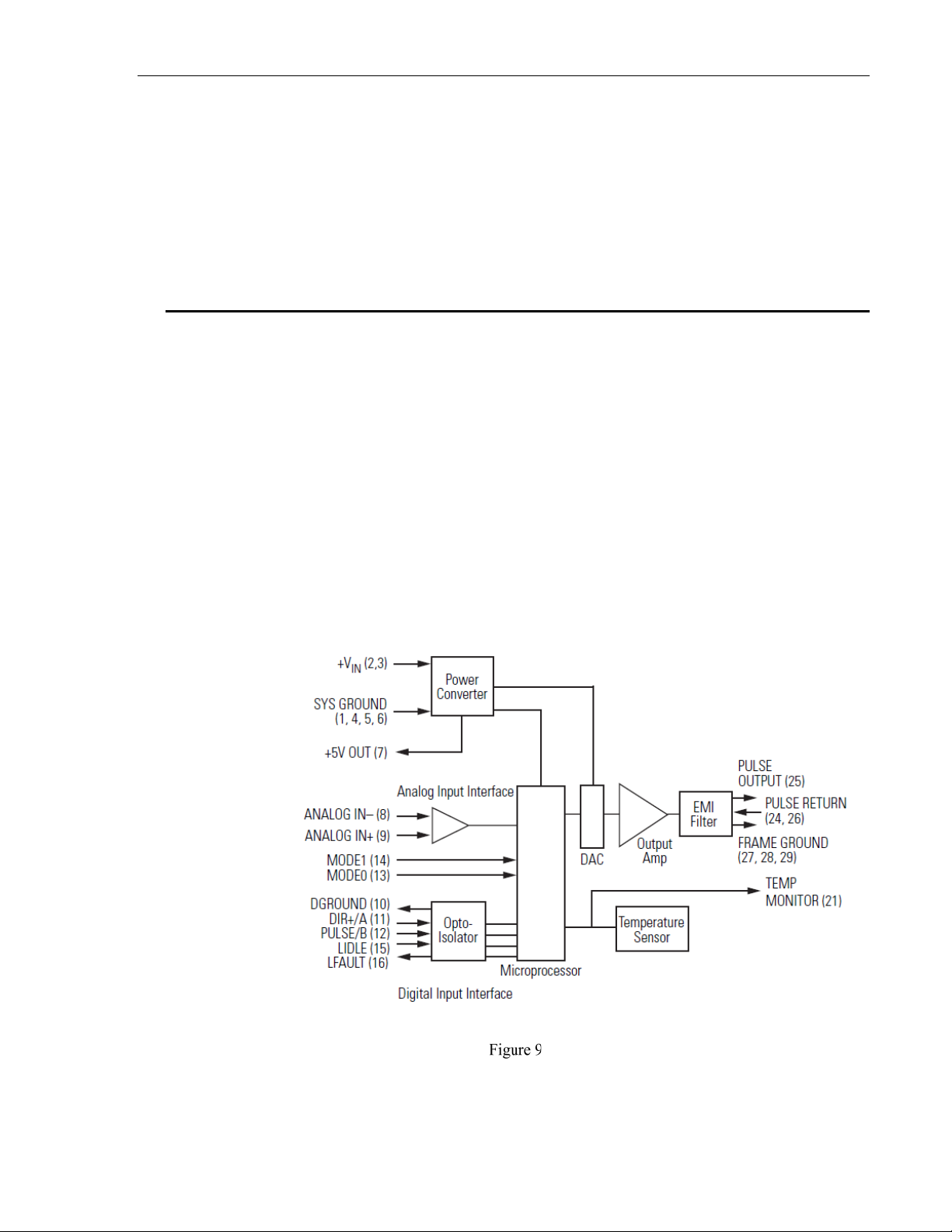
3.1 Block Diagram
The block diagram shows the basic design of the 8712. The microprocessor
reads the input mode bits when power is turned on and selects the input
interface. It also flashes the firmware version number on the internal red
LFAULT indicator. To check the firmware version, one has to count the
number of led flashes. There is a longer pause between the significant
number and the decimal number. For example, version 1.5 will flash the
LED once, followed by a pause, then will flash the LED five times.
Pulse and direction inputs (voltage or logic edge) from the selected interface
cause the microprocessor to generate low voltage Picomotor drive
waveforms. The output amplifier increases the amplitude of the drive
waveform sufficiently to drive the Picomotor. An internal power supply
generates the high voltage power for the output amplifier as well as other
supply voltages.
Block Diagram

10 Theory of Operation
When LIDLE is pulled low, the microprocessor shuts down the power supply
and stops generating Picomotor drive pulses. The response to this input is
rapid enough to prevent the generation of more than one pico pulse after
LIDLE goes low. Normal operation resumes after LIDLE is brought high.
3.2 Input Mode Control Bits
MODE0 and MODE1 are decoded when the power is applied. The interface
mode can only be changed by removing power to the 8712, then changing the
mode bits and applying power again. MODE0 and MODE1 define the control
interface as follows:
3.2.1 Step/Direction Mode
In this mode, DIR+/A is the direction input. PULSE+/B is the pulse
command input. TTL inputs to the control interface determine pulse
generation and the direction of motion. One Picomotor pulse is generated for
each falling edge of PULSE+/B. PULSE+/B can be left in either a high or
low state because it is edge sensitive. The low state is preferred because the
opto-coupler input diode will be off.
DIR+/A causes clockwise motion when high, and counter-clockwise motion
when low. It is checked before each pulse is made to allow instantaneous
direction reversal. DIR+/A is level sensitive, so it must be in the desired state
when PULSE+/B goes low and remain in that state for a minimum of 100 μs
after PULSE+/B goes low. The pulse rate can be between 0 and 2 kHz. Faster
pulse rates will not result in increased response.
3.2.2 Quadrature Mode
In this mode, DIR+/A is the A-phase input and the PULSE+/B is the B-phase
input. Like the step/direction mode, quadrature mode uses the digital control
interface. In this mode a pulse is generated for every edge transition of both
the A-phase and B-phase control inputs. The direction of motion is
determined by the phase of A with respect to B:
MODE0 MODE1 Description
0 0 Step/Direction Mode
1 0 Quadrature Mode
0 1 Line Voltage Input
1 1 Bang-Bang Voltage Input
This manual suits for next models
1
Table of contents
Other Newport DC Drive manuals


Popular DC Drive manuals by other brands


Danfoss
Danfoss VLT CDS 803 Design guide

Raymarine
Raymarine Mk II installation guide

KSB
KSB PumpDrive 2 Eco Application guide

SEW-Eurodrive
SEW-Eurodrive MOVIMOT MM D Series Compact operating instructions

Siemens
Siemens simovert masterdrives operating instructions

TR-Electronic
TR-Electronic MP-200 user manual