Nexite NXE-I945V(Versace) User manual

Hardware Document
nxtrdhw-001 R & D Team
Nexite, Inc. 1 /17 Revision 1.3
NXE-I945V(Versace) MotherBoard
Hardware Document
Apr 16. 2010
Written by SC Kim
Revision 1.3

Hardware Document
nxtrdhw-001 R & D Team
Nexite, Inc. 2 /17 Revision 1.3
Document Revision History
Released date Revision Description
Mar 21, 2008 Rev. 0.90 First prepared for this document.
This document describes the major specification of the NXE-
I945V(Versace) motherboard and the functional feature to be
extended by the customer.
The motherboard revision number is DVT
Mar 25, 2008 Rev. 0.91 Modified main title, general description and system overview
Modified a printed board name : Versace ÆNXE-I945V(Versace)
May 20, 2008 Rev. 1.00 Modified the rear port layout & configuration
Added 3Pin header for BIOS selection to board
Modified LVDS Pin Description (Added switched 12V)
Jun 30, 2008 Rev. 1.10 Modified LVDS Pin Description for Rev.C board
Nov 06, 2008 Rev. 1.20 GPIO pin 정의에 추가 보완.
Apr 16, 2010 Rev. 1.30 Modified PCB revision (C to D)
Some component has been changed ( CMOS Clear/IDE DOM Power)
User’s Notice
No part of this product, including the schematics and BIOS may be reproduced, transmitted, transcribed,
stored in a retrieval system, or translated into any language in any form by any means without the
express written permission of NEXITE Inc. except the document kept by the purchaser for backup
purposes.
© Copyright 2005 NEXITE Inc. All rights reserved

Hardware Document
nxtrdhw-001 R & D Team
Nexite, Inc. 3 /17 Revision 1.3
Contents of Table
I. Introduction
1. General Description ------------------------------------------------------------------------ 4
2. Functional Block Diagram ------------------------------------------------------------ 7
II. System Overview
1. NXE-I945V(Versace) Motherboard ------------------------------------------------- 7
2. Upgrade ability
2-1. Processor ----------------------------------------------------------------------------- 10
2-2. Memory -------------------------------------------------------------------------------- 10
2-3. BIOS ------------------------------------------------------------------------------------ 10
III. Jumpers , Connectors & Ports Descriptions
1. Board Jumpers Settings
1-1. Jumper description --------------------------------------------------------------- 11
2. I/O Headers , Slots & Connector Descriptions
2-1. Motherboard Internal Connectors ----------------------------------------- 12
2-1-1. Main connector, Slot & DIMM ------------------------------------------- 12
2-1-2. I/O Header & Connectors ------------------------------------------------ 13
3. Rear Ports Description ------------------------------------------------------------------- 16

Hardware Document
nxtrdhw-001 R & D Team
Nexite, Inc. 4 /17 Revision 1.3
I. Introduction
The NXE-I945V(Versace) motherboard offers a time-to-market consumer application solution featuring the Intel
Core2Duo and Conroe-L processor with the 1066/800/533 MHz system bus and Intel 945G & ICH7R Chipset.
Additional H/W platform features include integrated graphics controller core, DDR2 667/533/400 System memory,
Ultra ATA100, SATA2(3Gbps), Low Pin Count (LPC) interface, Universal Serial Bus 2.0, PCI, PCI audio solution
with HD audio CODEC, 4UART(RS-232C) port and controller, DVI and LVDS transmitters and ports(Rear and
Header) and Realtek Gigabit PCI Express Ethernet.
1. General description
θMain board
•PCB size in the special form factor
- 170mm * 170mm * 1.6T (10 Layers)
θProcessors
•LGA775 type processor and Standard heatsink.
•FSB 533/800/1066 supported
•Intel Core2Duo , Conroe-L processor
•Intel Pentium-4 / -D/ Celeron processor
θMain Chipset
•Graphic Memory Control Hub (GMCH) : Intel 945G
•I/O Control Hub (ICH) : Intel ICH7R (with RAID Function)
•LPC Controller : ITE8712F
•Ethernet controller : Realtek 8111B Gigabit PCI Ex Ethernet
•DVI Transmitter (SDVO to DVI) : Chrontel 7307C (QFP48P, SDVO-B)
•LVDS Transmitter (SDVO to LVDS) : Chrontel 7308B (QFP64P, SDVO-C)
•AudioSubsystem :RealTek ALC662 HD CODEC
•DC-DCSubsystem :Intersil ISL6326CRZ + ISL6612AECBZ (VRD11.0)
•ClockGenerator :ICS954101DGLF (TSSOP / CK410) + IDT2305 + ICS9DB603
•LPC to 4 UART controller : F81216D (48-LQFP)
θMemory Subsystem
•System Memory
- DDR2 667/533/400 memory types
- 3GB Maximum memory
- Bandwidth up to 10.7GB/s (DDR2 667) in dual channel Interleaved mode.
- Non-ECC memory only
- 256-Mb, 512-Mb and 1-Gb DDR2 technologies
•Flash Memory (SPI) : programmable 8 Mb Flash memory for BIOS
θIntegrated Graphics Device
•Core frequency of 400 MHz / 1.6 GP/s pixel rate
•Supports 8/16/32/64MB Frame Buffer sizes
•High-Quality 3D Setup and Render Engine
•High-Quality Texture Engine
•VLD/iDCT for enabling dual Intel High Definition streams for MPEG playback
θLPC to 4 UART Device
•Supports LPC interface
•Totally provides 4 UART (16550 asynchronous) ports
•Powered by 3Vcc
•48-LQFP(7mm x 7mm)
θAnalog Display Support
•400 MHz Integrated 24-bit RAMDAC
•Up to 2048x1536 @ 75 Hz refresh
•Hardware Color Cursor Support
•DDC2B Compliant Interface

Hardware Document
nxtrdhw-001 R & D Team
Nexite, Inc. 5 /17 Revision 1.3
θDVI Transmitter (Chrontel CH7307C)
•DVI (Digital Visual Interface) Transmitter up to 165M pixels/sec
•DVI Hot Plug detection
•Configuration through Intel Opcodes
•Onboard Integrated
•SDVO Port B Used
•DFP display at a pixel rate of up to 165MHz
•Supporting UXGA (1600x1200) resolution display
•DVI – I Connector used ( Integrated RGB + DVI output)
θLVDS Transmitter
•LVDS 18-bit and 24-bit outpus
•2D dither engine
•Panel protection and power sequencing
•High-speed SDVO serial AC-coupled differential RGB inputs
•Programmable power management
•SDVO Port C Used
•Single/Dual LVDS Transmitter up to 165Mpixels/s
•Panel fitting scalar, up-scale to a maximum resolution of 1920x1080
•Support OpenLDI and SPWG panel
•32Pin Header (2mm Pitch) for LVDS LCD Pannel Interface
θPCI Bus Interface
•Supports PCI Rev 2.3 Specification at 33 MHz
θFour LED display for POST progress
•User indicated Post progress & Error code
θIntegrated Serial ATA Host Controller
•Four ports
•Data transfer rates up to 3.0 Gb/s (SATA II)
•Integrated AHCI controller
θIntegrated IDE Controller
•Independent timing of up to two drives
•Ultra ATA/100/66/33, BMIDE and PIO modes
θUSB2.0
•Includes four UHCI Host Controllers, supporting eight external ports (USB 1.1 ports)
•Includes one EHCI Host Controller that supports all eight ports (USB 2.0 ports)
•Supports legacy Keyboard/Mouse software
θEthernet Subsystem (LAN – Realtek RTL8111B)
•Supports PCI Express 1.0a
•Integrated 10/100/1000 transceiver
•Auto-Negotiation with Next Page capability
•Supports Full Duplex flow control (IEEE 802.3x)
•Fully compliant with IEEE 802.3, IEEE 802.3u, IEEE 802.3ab
•Serial EEPROM
•Supports IEEE 802.1P Layer 2 Priority Encoding
•Transmit/Receive on-chip buffer (48KB) support

Hardware Document
nxtrdhw-001 R & D Team
Nexite, Inc. 6 /17 Revision 1.3
θSuper I/O Subsystem
•LPC Interface
•Motherboard GLUE Logic
•Keyboard Controller
- 8042 compatible for PS/2 keyboard and mouse
- Hardware KBC
- GateA20 and Keyboard reset output
•Extend GPIO Header
•Fan Speed controller
- Provides fan on-off and PWM control
- 128 steps of PWM modes
- Two Fan tachometer inputs
θAudio Subsystem
•RealTek ALC662 CODEC
- 5.1 Channel High Definition Audio Codec
- SPDIF out
- Three stereo DACs / Two stereo ADSs / Legacy analog input
- Six channel DAC supports 16/20/24-bit PCM format for 5.1 channel audio solution
- All DAC support independent 44.1k/48k/96kHz sample rate
- All ADC support independent 44.1k/48k/96kHz sample rate

Hardware Document
nxtrdhw-001 R & D Team
Nexite, Inc. 7 /17 Revision 1.3
2. Functional Block Diagram

Hardware Document
nxtrdhw-001 R & D Team
Nexite, Inc. 8 /17 Revision 1.3
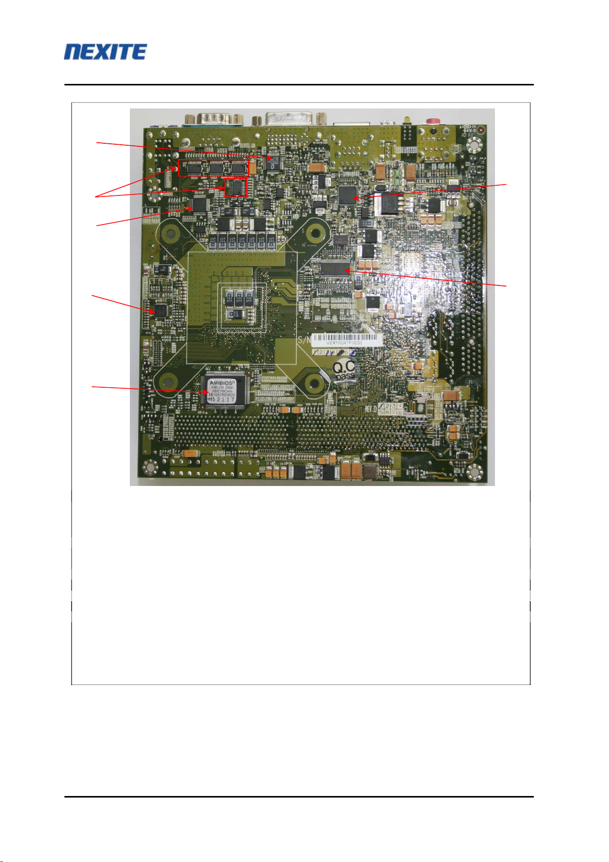
II. System Overview
1. NXE-I945V(Versace) Mother-Board
< NXE-I945V board Top side View >
1. HD Audio Codec : Realtek ALC662
2. SDVO to LVDS Transmitter : Chrontel CH7308B
3. Intel IO Control Hub : Intel NH82801GR ICH7R BGA-652
4. SPI Flash ROM(Socket) : MX25L8005M2C
5. ACPI Vol. Controller : Intersil ACPI Controller
6. CPU Core Vol. PWM FET : Fairchild FET
7. CPU Socket : LGA775 Core2Duo / Conroe-L
8. Graphic Memory Control Hub : Intel QG82945G GMCH BGA
1
2
7
4
3
8
6
5
Hardware Document
nxtrdhw-001 R & D Team
Nexite, Inc. 9 /17 Revision 1.3
< NXE-I945V board Bottom side View >
1. SDVO to DVI Transmitter : Chrontel CH7307C DVI Transmitter
2. RS-232C Line Drivers : TI GD75232
3. LPC to 4 UART : Fintek F81216D
4. 4-Phase PWM controller : Intersil ISL6326CRZ
5. LPC Super IO : ITE IT8712F-S
6. Gigabit Ethernet : RealTek RTL8111B
7. Clock Generator : ICS 954101DGLF
2
3
5
4 7
1
6

Hardware Document
nxtrdhw-001 R & D Team
Nexite, Inc. 10 /17 Revision 1.3
2. Upgradeability
2-1. Processor
User can upgrade CPU
- Core2Due / Conroe / Conroe-L / Pentium-4 / Pentium D / Celeron-D
2-2. Memory
The NXE-I945V(Versace) motherboard has two Dual Inline Memory Module (DIMM), minimum 256MB to
maximum 3GB memory size. The BIOS detects the memory type, size, and speed through SMBUS interface
between the core chipset and DIMM module automatically.
The motherboard supports the following memory features
•Maximum memory size : 3GB
•Directly supports one or two channels of memory (each channel consisting of 64 data lines)
•Supports DDR2 400, DDR2 533, and DDR2 667
•Available bandwidth up to 5.3 GB/s (DDR2 667) for single-channel mode or dual-channel asymmetric mode
and 10.7 GB/s (DDR2 667) in dual-channel Interleaved mode.
•Supports DDR2 memory DIMM frequencies of 400MHz, 533MHz, and 667MHz. The speed used in all
channels is the speed of the slowest DIMM in the system.
•Supports 256-Mb, 512Mb, and 1-Gb DDR2 technologies for x8 and x16 devices.
•Supports four banks for all DDR2 devices up to 512-Mbit density.
•DDR2-667 4-4-4 is Not supported
•Supports only unbuffered DIMMs.
•SPD (Serial Presence Detect) scheme for DIMM detection support.
•Supports configurations defined in the JEDEC DDR DIMM specification only
2-3 BIOS
θSPI Flash memory organization
The NXE-I945V(Versace) motherboard uses a AMI BIOS, which is stored in the flash memory and can be
upgraded using a disk-based or Windows-based program. An old version of the BIOS can be updated to the
newer version using the Flash Memory Update utility in a floppy diskette or HDD.

Hardware Document
nxtrdhw-001 R & D Team
Nexite, Inc. 11 /17 Revision 1.3
III. Jumpers , Connectors & Ports Descriptions
1. Board Jumpers Settings
1-1. Jumper Descriptions (2.54mm Pitch 3Pin Header)
* Note : Should be set the J4 jumper to 1-2 if it need to be supported LVDS Panel function.
Switch Function ◀▬(Left) ▬▶(Right) Remarks
SW1-2
CMOS Clear Function CMOS Clear Normal Default value :
▬▶(Right)
SW1-1 DOM Power supply CN24 IDE Connector
Pin 20 +5V Supplying Remove DOM
Power Default value :
▬▶(Right)
Jumper Function 1-2 2-3 Remarks
J4 LVDS Support
Option Supported the LVDS
Function Only DVI or RGB
(Not supported the
LVDS function)
Default value :
2-3(DVI)
J4
1
SW1
2
1
Hardware Document
nxtrdhw-001 R & D Team
Nexite, Inc. 12 /17 Revision 1.3
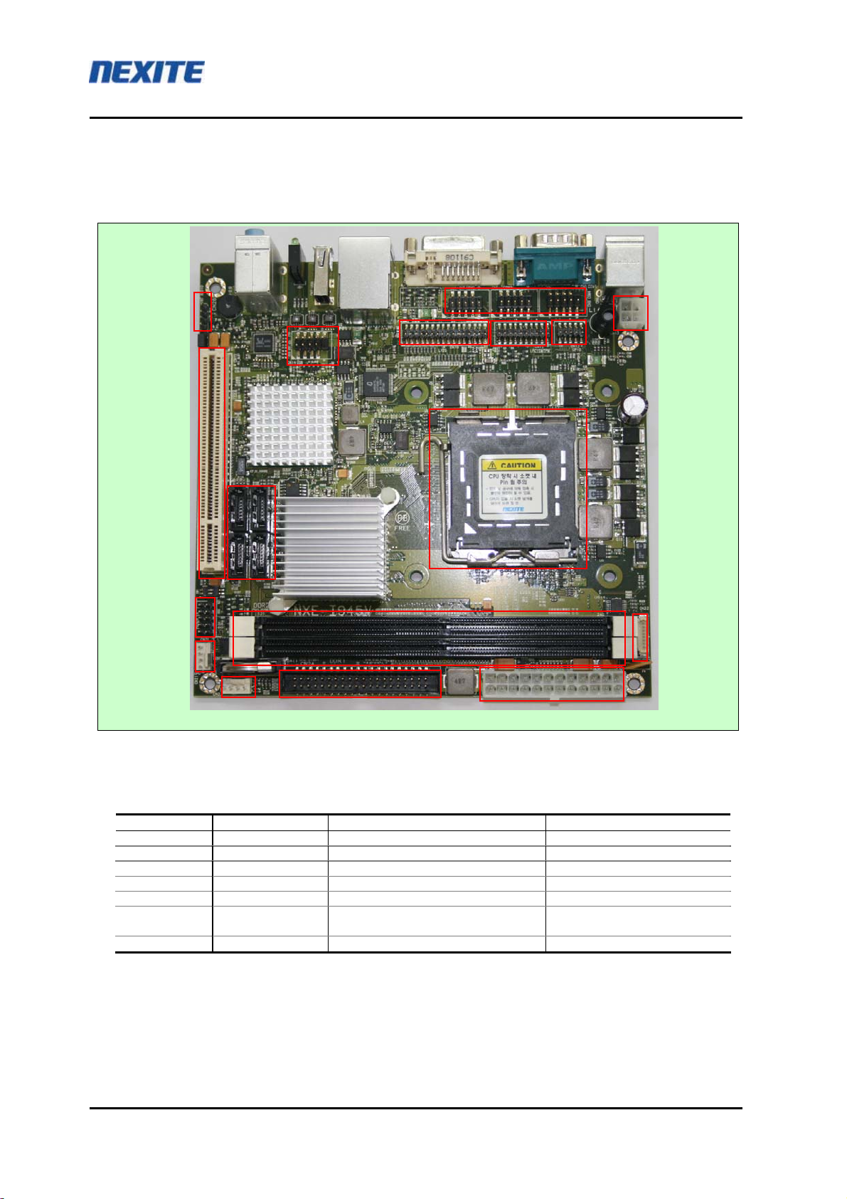
2. I/O Headers , Slots & Connectors Descriptions
2-1. Motherboard Internal Connectors
2-1-1. Main Connector, Slot & DIMM
No. Ref No. Description 1 Description 2
(06) CN13 4Pin 12V Power for CPU CPU Power 4 pin
(10) CPU1 LGA775 LGA775 CPU socket
(16) CN25 24Pin Main Power Main Power 24 pin
(12) DDR1 / DDR2 U : DDR2 == DDR1 : D DDR2 DIMM slots
(15) CN24 Pin20 : DOM Power (VCC) IDE connector
(09) CN16 ~ 19 L : CN16(Port0) || CN17(Port2) : R
L : CN18(Port1) || CN19(Port3) : R SATA II Connectors
(08) CN15 PCI slot PCI Slots
(02)
(08) (03) (05)
(04)
(07)
(01) (06)
(10)
(09)
(11)
(13)
(12)
(14) (15) (16)
(17)

Hardware Document
nxtrdhw-001 R & D Team
Nexite, Inc. 13 /17 Revision 1.3
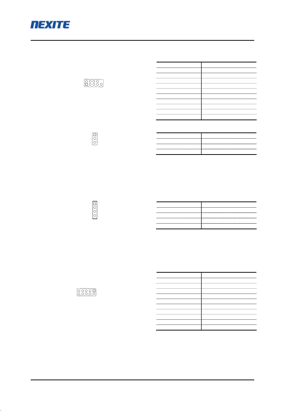
2-1-2. I/O Header & connectors
θ(13)/(14) : FAN connector (CN21:CPU FAN / CN23:SYSTEM FAN)
Pin number Signal description
1 GND
2 +12V
3 Encoder signal
4 PWM control signal
* Note : Should be connect the CPU FAN to CN21(CPU FAN Connector) if you want to exact FAN control
θ(11) : Front IO connector (CN20) – 2.54mm Pitch 10Pin Header
<Front IO Pin Header schematic>
θ(07) : USB2.0 interface connector(CN14) – 2.54mm Pitch 9Pin Header
Pin number Signal description
1 HDD LED +
3 HDD LED -
2 Power LED +
4 Power LED -
5 Power BT(-)
7 Power BT
6 System Reset(-)
8 System Reset
9 Ground
10 N.C
Pin number Signal description
1 VCC1
3 USB1-
5 USB1+
7 GND1
2 VCC2
4 USB2-
6 USB2+
8 GND2
9 Key PIN (NC)
10 GND
1 2 3 4
CN21/CN23
1
Æ
9
Æ
Å
2
Å
10
1
Æ
Å
10
2
Æ
Hardware Document
nxtrdhw-001 R & D Team
Nexite, Inc. 14 /17 Revision 1.3
θ(02) : Internal Serial(RS-232) Pin Header (CN7 / CN8 / CN9) – 2.54mm Pitch 9Pin Header
θ(01) : SPDIF Pin Header (J1) – 2.54mm Pitch 3Pin Header (~up to PCB Rev.C)
* Note : To use the SPDIF function , needed a external Optical or Coaxial connector for SPDIF output
θ(01) : Internal Line-out Pin Header (CN26) – 2.54mm Pitch 4Pin Header
This pin header had supported at the PCB Rev.D.
The SPDIF header had no more supported on the PCB Rev.D
Note: The analog audio signal of CN26 had shared with Line-out signal of CN1(3-stack audio)
θ(05) : General Purpose Input / Output (GPIO) Pin Header (CN12) – 2mm Pitch 10Pin Header
Pin number Signal description
1 -DCD
3 RXD
5 TXD
7 -DTR
9 GND
2 -DSR
4 -RTS
6 -CTS
8 -RI
10 KEY
Pin number Signal description
1 VCC (5V)
2 SPDIF OUT
3 Ground
Pin number Signal description
1 Line-out Right Audio
2 Ground
3 Ground
4 Line-out Left Audio
Pin number Signal description
1 VCC3 (+3.3 Volt)
2 SIO GP24 (Input)
3 SIO GP20 (Output)
4 SIO GP25 (Input)
5 SIO GP21 (Output)
6 SIO GP26 (Input)
7 SIO GP22 (Output)
8 SIO GP27 (Input)
9 SIO GP23 (Output)
10 Ground (GND)
2
Æ
Å
9
1
Æ
1
Æ
9
Æ
10
Æ
Å
1
Å
2
[Note]
GPI[Input]
를
사용하기
위해서는
,
상대
시스템
의
Output
단은
Open-drain output
특성을
갖는
pin
을
사용하면
,
반드시
Output
단에
Pull-up
되어
있어
야
합니다
1
Æ

Hardware Document
nxtrdhw-001 R & D Team
Nexite, Inc. 15 /17 Revision 1.3
θ(04) : TPM and LPC Extension Header (CN11) – 2mm Pitch 20Pin Header
Pin number Signal description
1 VCC3 (+3.3 Volt)
2 VCC3 (+3.3 Volt)
3 -LPC FRAME (LPC IF)
4 VCC (+5 Volt)
5 LPC AD3 (LPC IF)
6 VCC (+5 Volt)
7 LPC AD2 (LPC IF)
8 +12V
9 LPC AD1 (LPC IF)
10 -12V
11 LPC AD0 (LPC IF)
12 TPM GPIO0
13 -PLTRST (PCI Reset)
14 PCLK3 (33MHz clock)
15 SER IRQ (Serial IRQ)
16 Ground (GND)
17 PCLK2 (33MHz clock)
18 CLK48_ETC (48MHz clock)
19 Ground (GND)
20 Ground (GND)
19
Æ
20
Æ
Å
1
Å
2

Hardware Document
nxtrdhw-001 R & D Team
Nexite, Inc. 16 /17 Revision 1.3
θ(03) : LVDS Interface PIN Header (CN10) – 2mm Pitch 32Pin Header
θ(17) : LCD Backlight Control connector (CN22)
Pin number Signal description
1 +12V
2 +12V
3 +12V
4 Enable Backlight
5 (note2) Control (VCC or GND)
6 Ground
7 Ground
8 Ground
* Note1 : Connector Part No. Æ12505WS – 08A00
* Note2 : Pin 5(Default 10Kohm pull-up to VCC(5V))
Pin number Signal description
1 LVDS Data0 N
2 LVDS Data0 P
3 LVDS Data1 N
4 LVDS Data1 P
5 LVDS Data2 N
6 LVDS Data2 P
7 Ground (GND)
8 LVDS Clock Channel1 N
9 LVDS Clock Channel1 P
10 LVDS Data3 N
11 LVDS Data3 P
12 LVDS Data4 N
13 LVDS Data4 P
14 Ground (GND)
15 LVDS Data5 N
16 LVDS Data5 P
17 Ground (GND)
18 LVDS Data6 N
19 LVDS Data6 P
20 LVDS Data7 N
21 LVDS Data7 P
22 LVDS Clock Channel2 N
23 LVDS Clock Channel2 P
24 Ground (GND)
25 +3.3V (LCD Panel Power)
26 4.7Kohm to Ground
27 +5V(LCD Panel Power)
28 +5V (LCD Panel Power)
29 +3.3V (LCD Panel Power)
30 +3.3V (LCD Panel Power)
31 +12V (LCD Panel Power)
32 +12V (LCD Panel Power)
2
Æ
1
Æ
Å
32
Å
31
1 Æ
[Note]
The LVDS pair signals should be twisted with
ground shield for EMI Radiation & Signal
quality.
Hardware Document
nxtrdhw-001 R & D Team
Nexite, Inc. 17 /17 Revision 1.3
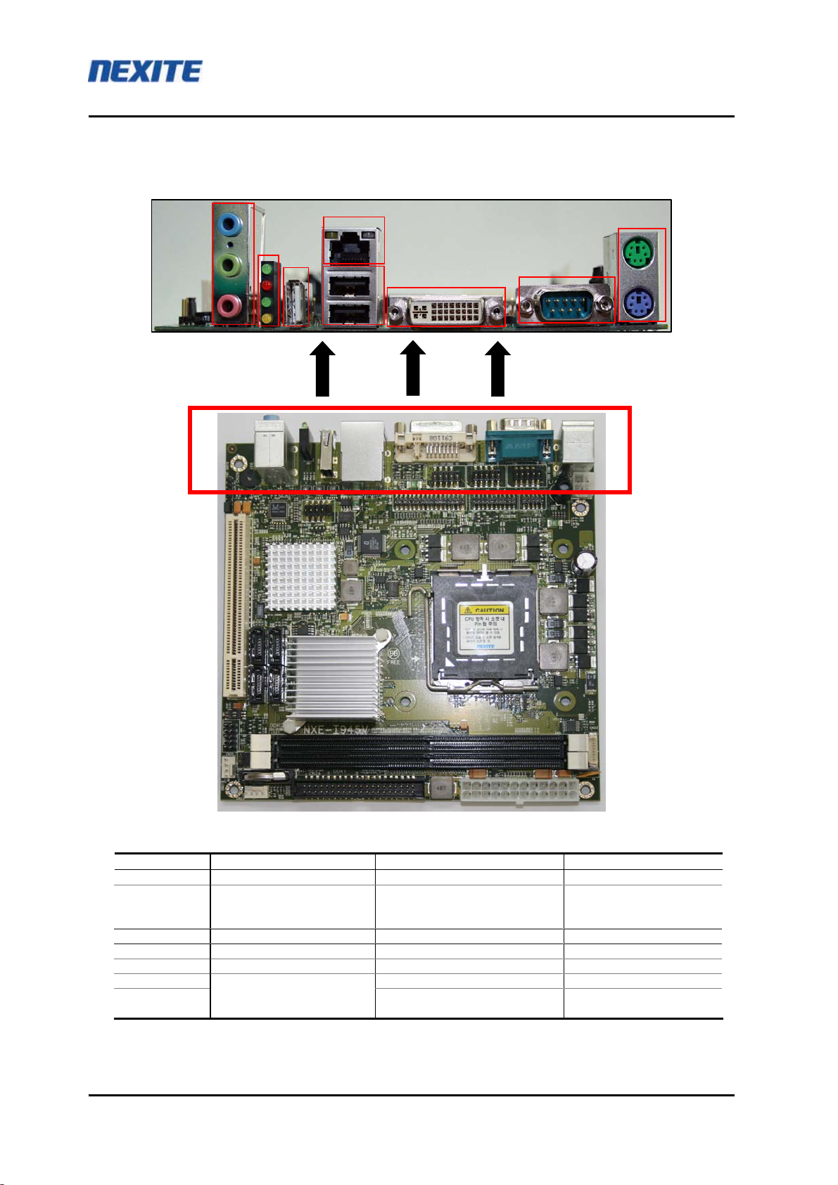
3. Rear Ports Description
No. Functions Description 1 Description 2
(1) POST LED Display POST Sequence LED1
(2) HD Audio Port Blue : Line In
Green : Line Out
Pink : Microphone
Blue : Surround out R/L
Green : Front out R/L
Pink : Center / LFE out
(3) (5) USB 2.0 Ports USB 2.0 3Ports CN2 / CN3
(4) RJ45 Ethernet connector Gigabit Ethernet Connector CN3
(6) DVI-I Graphic Port DVI + Analog RGB CN4
(7) RS-232 Serial Port 9Pin D-sub serial port CN5
(8) PS/2 Keyboard / Mouse
Port Green : Mouse Port
Violet : Keyboard Port CN6
(1)
(2)
(3)
(5)
(4)
(6) (7)
(8)
Table of contents
Other Nexite Motherboard manuals


