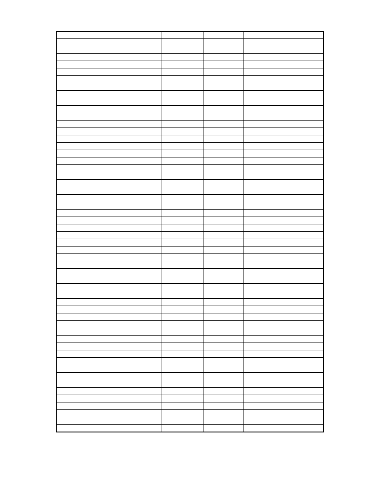
Nokia 447ZiPlus User manual

ZB1730
01.00
When re---ordering manuals, please quote the model name and part number.
xx
Nokia Display Products Oy
P. O . B o x 1 4
FIN---24101 Salo, Finland
17” Colour Monitor 447ZiPlus

447R
2

1
TABLE OF CONTENTS
PAGE
1. Precautions and notices------------------------------------------ 2
2. Specification----------------------------------------------------------4
3. Control Location and Functions---------------------------------5
4. Disassembly instructions----------------------------------------- 7
5. General Connections & applications---------------------------9
6. Electronic Circuit Description------------------------------------10
7. Adjustment----------------------------------------------------------- 21
8. Troubleshooting follow Chart------------------------------------ 27
9. Block Diagram-------------------------------------------------------34
11. Circuit Diagram-----------------------------------------------------35
10. PCB Layout----------------------------------------------------------37
12. Mechanical Disassembly-----------------------------------------39
13. Mechanical Parts List---------------------------------------------40
14. Electrical Parts List------------------------------------------------41

2
1. PRECAUTIONS AND NOTICES
1-1 SAFETY PRECAUTIONS
1) Observe all cautions and safety related notes located inside the display cabinet and on the display
chassis.
2) Operation of these displays with the cabinet removed involves a safety hazard from electric shock.
Work on the display should not be attempted by anyone who is not thoroughly familiar with
precautions necessary when working on high voltage equipment.
3) Do not install remove or handle the picture tube in any manner unless shatter-proof goggles are
worn. People not so equipped should be kept away while handing picture tube. Keep picture tube
away from the body while handing.
4) The picture tube is constructed to limit X-RADIATION to 0.5MR/HR.at 300 mA anode current. For
continued protection, use the recommended replacement tube only, and adjust the voltages so that
the designated maximum rating at the anode will not be exceeded.
5) Before returning a serviced display to the customer a thorough safety test must be performed to
verify that the display is safe to operate without danger or shock. Always perform an AC leakage
current check on the exposed metallic parts of the cabinet. Proceed as follows.
Connect the monitor power lead to the mains supply, via an isolation transformer, and switch on,
Using the test circuit shown in Fig1-1 measure the AC leakage current between each pole (L and
N) of the supply and all accessible metal parts. The earth leakage current must not exceed 3.5mA
(Fig 1-1)

3
1-2 product safety notice
Many electrical and mechanical parts in this chassis provide special visual safety protection. The
protection afforded by them cannot necessarily be obtained by using replacement components rated
for higher voltage. wattage. etc..
Before replacing any of these components. read the parts list in this manual carefully. The use of
substitute replacement parts which do not have the same safety characteristics as specified in the
parts list may create shock, fire.
X-RAY radiation or other hazards.
1-3 service notes
1) When replacing parts or circuit boards. wrap the wires around terminals before soldering.
2) When replacing a high wattage resistor (more than 1/2W) on a circuit board keep the resistor
about 10mm (1/2 in ) away from circuit board.
3) Keep wires away from high voltage or high temperature components.
4) Keep wires in their original position so as to reduce interference.
Specifically for the cancellation wires of the TCO electric field emissions reduction purpose. This
black cancellation wire is taken and connected from the maim chassis connector P500 through a
wire clip which fixed on the heat sink of flyback transformer. Then get this wire underneath the round
rotation coil, soldering on the left-hand side of the copper pad which fitted around the red circle of the
anode connection on the tube back.
Also, care must be taken for the I2C wires from P903A(on the main Board) to P904(on the CDT drive
Board).
This white color and red color wires combined flat wire are used for I2C communication.
It should be fixed on the left side and rear side of FBT heat-sink by clip wires in order to keep away
from the Deflection wires. High Voltage wire (red) and two focus wires (red and white) from FBT,
because I2C are very easy to pick up noise from those wires and caused wrong color or wrong
contrast.

4
Time Table For Sync. Signal
Mode No. 1 2 3 4 Unit
Resolution 720 x 400 640 x 480 640 x 480 800 x 600
Horizontal Frequency 31.468 31.469 43.269 37.879 KHz
(A)Horizontal 31.774 31.778 23.11 26.4 usec
(B ) Horizontal Pulse 3.813 3.813 1.556 3.2 usec
(C ) Horizontal Back Porch 1.907 1.907 2.222 2.2 usec
(D) Horizontal Active Area 25.423 25.422 17.778 20 usec
(E) Horizontal Front Porch 0.325 0.636 1.554 1 usec
(F) H. Sync. Polarity - - - +
Vertical Frequency 70 59.94 85.008 60.317 Hz
(O) Vertical Period 14.286 16.683 11.764 16.570 msec
(P) Vertical Pulse Width 0.063 0.064 0.069 0.106 msec
(Q) Vertical Back Porch 1.143 1.049 0.578 0.607 msec
(R )Vertical Active Area 12.698 15.253 11.093 15.840 msec
(S) Vertical Front Porch 0.382 0.317 0.024 0.026 msec
(T) V. Sync. Polarity + - - +
(U) Interlaced No No No No
Mode No. 5 6 7 8 Unit
Resolution 800 x 600 832 x 624 1024 x 768 1024 x 768
Horizontal Frequency 53.674 49.725 48.363 68.677 KHz
(A)Horizontal 18.631 20.113 20.677 14.561 usec
(B) Horizontal Pulse Width 1,138 1.117 2.092 1.016 usec
(C) Horizontal Back Porch 2.702 3.911 2.462 2.201 usec
(D) Horizontal Active Area 14.222 14.522 15.754 10.836 usec
(E) Horizontal Front Porch 0.569 0.558 0.561 0.508 usec
(F) H. Sync. Polarity + - - +
Vertical Frequency 85.061 74.5 60.024 84.989 Hz
(O) Vertical Period 11.756 13.416 16.660 11.765 Msec
(P) Vertical Pulse Width 0.056 0.060 0.124 0.044 Msec
(Q) Vertical Back Porch 0.503 0.784 0.600 0.524 Msec
(R ) Vertical Active Area 11.199 12.551 15.880 11.183 Msec
(S) Vertical Front Porch 0.019 0.021 0.062 0.014 Msec
(T) V. Sync. Polarity + - - +
(U) Interlaced No No No No No
Mode No. 9 10 Unit
Resolution 1152 x 864 1280 x 1024
Horizontal Frequency 67.5 69.095 KHz
(A)Horizontal 14.815 14.473 usec
(B) Horizontal Pulse Width 1.185 1.160 usec
( C) Horizontal Back Porch 2.370 2.219 usec
(D) Horizontal Active Area 10.667 10.758 usec
(E) Horizontal Front Porch 0.593 0.33 usec
(F) H. Sync. Polarity + +
Vertical Frequency 75 65 Hz
(O) Vertical Period 13.333 15.385 msec
(P) Vertical Pulse Width 0.044 0.043 msec
(Q) Vertical Back Porch 0.474 0.567 msec
(R ) Vertical Active Area 12.8 14.82 msec
(S) Vertical Front Porch 0.015 0.041 msec
(T) V. Sync. Polarity + +
(U) Interlaced No No

5
3. Control Location and Functions
FRONT
Down/Brightness Key
Select Key
Up/contrast key
Power LED
Power Switch

6
Controls on front panel Function
1. Power LED
This indicator will light when the power cord is properly connected and the power switch is ON.
The state of the LED is dependent on the Power State of the monitor. When the LED is green, the
monitor is in the normal state. When it is yellow or amber, it indicates a power saving state.
2. Power Switch
Press to power on the monitor; press again to power off.
We recommend to power your system on first, then the monitor.
3. Select
Press MENU key to reveal the OSD menu which include the sub-menu of the arrow headed item in the
lower half part of the OSD window.
The arrow headed item can be selected by pressing either of + key or - key to move the yellow shadow
bar to the function item which to be selected.
When the yellow shadow bar move to the function of submenu, press the select key, OSD will address
to the adjustment of that certain function, by pressing and hold down either of the + key to increase or –
key to decrease the function setting.
4. +/- Key
Other than above functions, + key can also be direct access for the contrast adjustment, whereas – key
is direct access for the brightness adjustment.

7
4. Disassembly Instructions
Disassembly Instructions
1. Face Down The Monitor (Fig 4-1).
2. Back Cover Removal
a) Use small flat bladed screwdriver suitably protected against cabinet damage insert into the four
respective crevices Fig 4-2 ”A” where located on the crevices lateral side of the unit in the seam of
the back & front cover, hold and push the clip down to ease the snap – on lock.
b) Remove the back cover.
c) Unplug the DY connector, AC connector, Degaussing coil connector and the CRT grounding
connector from
the FBT shield.
d) Discharge the remaining static electricity by shorting CRT anode to ground. Then remove the FBT
anode connector (Fig.4-3).
e) Remove the PC main board form sliders of the
front cover (Fig.4-4).
3. PCB Assembly Remove
Caution : When servicing or replacing the CRT Disconnect the Anode and Discharge the Anode
shield completely. As high voltage (26kV) may remain on the Anode for an extended time
after power off.
Fig 4-1 Fig 4-2
A
A
A
A

8
Fig.4-3
Fig.4-4

9
5. General Connection & Applications
Procedure for installing and using this model of ultra Super-VGA color display.
1. Set up the display at the desired operation location , on top of or beside your personal computer. Plug the
power cord into the monitor and then connect the other end of the power cord into an AC outlet. The
three-wire power cord is provided as a Safety Precautions to ensure proper electrical grounding.
2. Signal cable 15 pin D sub connector pin assignment:
Pin assignment Description
1Red
2 Green
3Blue
4 Ground
5 Ground
6 Red Ground
7 Green Ground
8 Blue Ground
9 NOT Connected
10 Ground
11 ID O(tie to LG)
12 SDA
13 H.Sync
14 V.Sync
15 SCL
3. First turn the PC power switch ON. Then apply power to the display by pressing the power ON/OFF
switch to power on monitor. The power indicator light will illuminate. Allow about thirty seconds for the
display tube to warm up , data will be displayed on screen.
4. Adjust the BRIGHTNESS and CONTRAST controls for the best readability. Adjust the H.Width and
H.Position control as necessary for proper horizontal display.
5. V. Height can be adjusted to give you a proportional vertical display.
NOTE :1. If your extended VGA color display requires service. Refer to the control and adjustment
information in this publication and verify that all controls and adjustment of the display are
properly set.
2. If your display does require service it must be returned with the power cord.

10
6. ELECTRONIC CIRCUIT DESCRIPTION
6-1. Switching Mode Power Supply (SMPS)
The switching mode power supply for this monitor is a full range type.
Universal power input of ac 100V … 240V is compatible.
The AC input is supplied through the slow blow fuse F801, the first line filter T802, the second line filter
T803 to the rectifier D811 …D814.
The rectified DC voltage is about 125V … 335V and is fed to the switching transformer T801 via R808.
Prior to start, small current flows to C866A via R849, R850, Q850.I862 is to operate immediately
when the voltage across C866A reaches 16V. At the same time, Q868 is on, the rectified current
flows through the primary winding of T801 and the energy is stored in it.
When Q868 is off, the energy is transferred to the secondary winding, the auxiliary winding is close -
coupled and in phase with the secondary winding, it will provide a holding voltage on C866A and fed to
pin 7 of I862 via R831 , D831,D870 I862 will keep working provided that voltage across C866A is over
10V.
The oscillating frequency of the switching mode power supply is around 30KHz, which is determined by
the timing components R861, C863.
Capacitor C863 is charged to 2.8V via the 5V reference voltage on pin8 of I862 and discharge to 1.2V,
during the discharge time interval, the oscillator generates a series of blanking pulses which cause the
output at pin6 of I862 to go low.
The fly-back pulse from T440 is buffered by R864 and differentiated by C864, R863. A sharp pulse is thus
obtained to force C863 to discharge, so that the oscillating frequency is synchronized and kept in phase
with that of horizontal frequency to avoid interference on the display screen.
Should the voltage vary due to the charge of input AC or output loading, the auxiliary winding will reflect
these variation to pin2 of I862 via D831, R831, R835. The voltage at pin2 of I862 is compared with the
internal 2.5V reference voltage to produce an error voltage which is limited to 1V by internal zener diode.
The comparator output is then compared with the voltage at pin3 of I862 which is supplied from the
voltage detected across R867, while Q868 is on. Q868 is off only when the voltage drop across R867 has
reached that of the error voltage, or1 V p-p maximum.
The error voltage controls the duty cycle of the pulse width modulator to regulate the output
voltage.
If over-load or short circuit occurs at the secondary, the voltage across R867 reaches 1 V p-p rapidly,

11
thereby blocking the power output, the voltage at pin7 of I862 then decrease to below 10V, I862 is forced off.
However, in order to allow auto-recovery from power saving off state, the SMPS circuit is designed as an
unlatched type, the DC current flows via R849 Q850, R850 to charge C866A again, when the voltage across
C866A has reached 16V, I862 is turned on again. Once the peak voltage across R867 is over 1Vp-p, I862
will be forced off again.
Consequently, when short circuit or overload occurred, I862 is turned on and off repeatedly, and the power
will not be switched off, Q868 and R808 may be over stressed and fail.
6-2 Power Management Circuit
There are three modes of indicator in this power LED described as below, the first mode, “green-
indicator “ indicates the normal state; “yellow-indicator“ indicates the stand-by and the suspend
state. The third mode, “ amber-indicator “ indicates the power saving off state. Both H. sync and V.
sync are off.
I501
MODE
#40
V
#39
H
#31 #29 D862
LED
NORMAL 1111GREEN
STANDBY 1001YELLOW
SUSPEND 0101YELLOW
OFF 0000AMBER
When the display signal enters the “suspend “ state of power saving, which is V. sync off, the voltage at
pin31 of I501 is low, Q821 is OFF, and Q820 is OFF too. this will shut down the oscillation of the horizontal
and vertical deflection , the power saving is then achieved.

12
When the display signal enters the “ off ” state of power saving which both H. sync and V. sync off,
the voltage at pin31& pin 29 of I501 are low, then Q820 is off and Q822 is off too, there is no 8V &
14V Voltage for the circuit.
The overall power dissipation is significantly reduced to less than 5 watts.
To recover from off state to normal state is automatic since the recoved H. sync and V. sync will
trigger I501 via Q550 &Q556, The voltage on pin 29 & 31 will go to high again and turn on Q822,
Q820 via Q823, Q821.
Heater voltage
The heater element in the CRT is supplied with 6.3+0.3V during normal operation of the monitor and
5.0+0.5v during suspend mode. To achieve the goal, Q851, D871 and associate circuit are introduced
when at normal state, a Horizontal pulse is fed to D871 via P807, Q851 is on, the feedback voltage on pin
2 of I862 is normal, the output voltage of the secondary side of T801 is normal the heater voltage is 6.3V +
0.3V.
Horizontal output is shut down by making Q820 off during suspend state. There is no Horizontal pulse
then Q851 is OFF. The feedback voltage is higher than the normal state. this will force the output voltage
of the secondary side of T801 drop down. With the right value of R800, R832, R833, the heater voltage
will be 5.0+0.5V
6-3. Automatic and Manual Degaussing Circuit
When power switch getting started, MCU #38 will send out a "high" signal to turn on Q801. Simultaneously
a current flows from B+(14V) via R807 and SR801 to make the relay on, the posistor R806 and the
degaussing coil L901 constitutes an automatic degaussing circuit to demagnetize the shadow mask and
the internal shield of the CRT in order to protect the display screen from color impurity.
The resistance value of the posistor is as low as 14 ohm during power off.
Immediately after the display turned on, a large AC current flows through the resistor into the degaussing
coil for demagnetization.
AT the same time, the resistor value of the posistor increase rapidly due to
the rise of its temperature, the degaussing current thus decreases to less than 100mAp-p in a few
seconds so that the display screen settles quickly, when the degaussing function is finished.

13
To manually degauss, it can be operated by selecting " " from the OSD
Menu and pressing MENU select key , it is similar to auto-degaussing.
MCU will be signaling a "high" level to Q801 , hence the manual degaussing is activated.
OSD lock / unlock function
When the degauss icon “ “ is pressing more then 10 seconds, the OSD menu will be forced to enter
OSD lock mode and will not allow function setting.
When OSD is at lock mode, selecting “ “icon from OSD and then press it more than 10 seconds
again, the lock mode will be forced to release and back to the normal.
6-4. Micro-Control Circuit
The monitor uses an advanced CPU (I501) to control the H. center; V. center V. height , pincushion,
trapezoid and so on by I2C BUS.
The horizontal sync and vertical sync are buffered by Q550, Q556 and fed to pin39, pin40 of I501, the
output sync signals are fed to pin1, and pin2 of deflection processor I401 via pin33, pin32 of I501.
With the H. size control signal, the PWM control signal is derived from pin2 of I501 which is fed into a
integration circuit R503, C503 and pull-up resistor R502 and amplifier Q502 to give a DC control voltage
on the collector of Q502.
The CPU is reset when the power cable is re-plug in. The components R506, D506 and C506 on pin4 of
I501 ensure correct start.
The +5V voltage is fed into I501 via pin5, a 8MHz resonator is connected on pin7, pin8 of I501 to generate
the CPU clock for the software execution. There are four input keypads S00 to S04. When a key is
pressed, the corresponding input port will be shorted.
The linearity control signal of horizontal circuit are derived from pin16, pin17, pin20, and pin22 which are
fed to Q402; Q404; Q480 for CS correction and Q489 for linearity C correction.

14
The table below describes the relationship between CS logic and horizontal frequency.
hf <33khz 34 to 39 khz 40 to 44 khz 45 to 51khz 52 to 61 khz Hf > 62 khz
Cs0
(Linearity S
correction)
L H L H L H
Cs1
(Linearity S
correction)
L H L L H H
Cs2
(Linearity S
correction)
L L H H H H
Cs3
(Linearity C
correction)
H H L L L L
There is a low power override pin on pin30 of I501 this pin is pulled-up to 12V by R984, R986 on drive board
PWB-0170 and connected to pin5 of the signal cable. When the signal cable is disconnected from the
computer, this pin is high and the Self-test pattern will work as described below
When you disconnect the signal cable from the PC, and power on the monitor, the display will produce a
moving square self-test pattern. The self-test function is useful to confirm the monitor is working correctly.
When the signal cable is connected to the unpowered computer, this pin is low and the power saving circuit
will be operated, the CPU will generate a power saving signal on pin29 & pin31 of I501
The monitor is design to have the DDC 1/2b functions, communication between |the monitor and computer
for DDC is via pins24, 25 of I501 which are defined as SDA, SCL signals. The computer will read out the
EDID data from the EEPROM I502 via I2C data lines. The EDID data is written into the EEPROM in the
factory during production.
The memory size for EDID data is 128 bytes shared from EEPROM I502 which has 8K bytes memory size.
6-5. How to enter into the factory setting:
The monitor includes 10 sets of factory preset timings although only some of the timings are fine-tuned by
auto alignment during production.
Switch off the monitor, push and hold down the "select" key and power on again, wait 1.0 second then
release the "select" key, the monitor should now be in the factory setting mode. (OSD in blue background) ,
All adjustment data will be stored automatically , then power on again , the monitor will revert to normal
operating state.

15
6-6. Deflection Processor
I401 TDA9111 is an SGS monolithic integrated circuit assembled in a 32 pins shrunk dual in line plastic
package.
I401 controls all the function related to the horizontal and vertical deflection in a multi-sync monitor.
As can be seen in the block diagram, I401 includes the following function:
Auto-sync and auto-processing for positive or negative H. /V. sync polarities on pin 1-2.
East/West pincushion signal processing on pin 24.
B+control, on pin14-17, 28.
H.PLL lock/unlock identification on pin 8 and safety blanking output on pin12.
X-ray protection is on pin 25.
I401 combined with I330 (TDA8172)which is a vertical booster to drive the vertical deflection yoke.
6-7. Pin -Out Description for SGS TDA9109 (I401)
Pin
No
Name Function
1 H-SYNC TTL Horizontal Sync Input
2 V-SYNC TTL Vertical Sync Input
3 HLOCKOUT First PLL Lock/Unlock Output (0V unlock -5V locked)
4 PLL2C Second PLL Loop Filter
5 Co Horizontal Oscillator Capacitor
6 Ro Horizontal Oscillator Resistor
7 PLL1-F First PLL Loop Filter
8 HLOCK-CAP First PLL Lock /Unlock Time Constant Capacitor
9 HFOCUSCAP Horizontal Dynamic Focus Oscillator Capacitor
10 FOCUSOUT Mixed Horizontal and Vertical Dynamic Focus Output
If this Pin is Ground, the H. and V. Output are Inhibited.
11 H-GND Horizontal Section Ground
12 H-FLY Horizontal Fly-back Input ( Positive Polarity )
13 H-REF Horizontal Section Reference Voltage ,8V
14 COMP B+ Error Amplifier Output for Frequency Compensation & Gain Setting
15 REGIN Regulation Input of B+ Control Loop
16 I-SENSE Sensing of External B+ Switching MOSFET Q440 Source Current
17 B+GND Ground(related to B+ reference adjustment)
18 BREATH DC Breathing Input Control
19 V-GND Vertical Selection Signal Ground
20 VAGC-CAP Memory Capacitor for Vertical AUTO-GAIN Control Loop in Vertical
Ramp Generator

16
21 VREF Vertical Section Reference Voltage (to be filtered)
22 V-CAP Vertical Saw-tooth Generator Capacitor
23 V-OUT Vertical Ramp Output ( With frequency independent amplitude and S or
C Corrections if any) It is mixed with vertical position reference voltage
output and vertical moiré)
24 E/W-OUT East/West Pincushion Correction Parabola Output
25 X-RAY X-RAY Protection Input(With Internal Latch Function
26 H-OUT Horizontal Drive Output (Collector of internal Transistor )
27 GND General Ground (reference to Vcc)
28 B+ OUT B+ PWM Regulator Output
29 Vcc Supply Voltage( 12V )
30 SCL I2C Clock Input
31 SDL I2C Data Input
32 5V Supply Voltage (5V)
6-8. Vertical Deflection Circuit
The power amplifier driving the vertical yoke assembly is a DC design-based on power amplifier I330
TDA8172.
The vertical deflection coil is connected to pin5 of I330 via P440. The saw-tooth signal is derived from
pin23 of I401 and fed to pin1 of I330 via R330 / C330. The DC bias voltage is derived from pin21 of I401
and fed to pin7 of I330 via derived R347 / R348 to optimize the vertical position. R335 /C336 is to
stabilize the power amplifier output.
There are two supply voltage for I330, -9V is applied at pin4 via R334, +14V DC voltage is applied at
pin2 and pin6 via D344 for the output stage during the retrace time. The supply voltage for the output
stage during the retrace time is derived from the fly-back generator output on pin3 of I330 and applied
through C343 to pin6 of I330.

17
6-9. Horizontal Deflection Circuit
Q429 is switched by the horizontal drive signal from pin26 of I401 via level-shift components R424,
C427, and D428. This produces a sufficient voltage to drive T430, Snubber network R429, C429
compensates for leakage inductance in T430 and shapes the base drive waveform.
The drive signal is fed to Q433 via D431, R431. When Q433 is at the “ off “ state, the changes stored
on the base and collector of Q433 will discharge via D431.By this way, switching loss will be reduced.
The drive signal controls Q433 to switch on and off, so that saw-tooth waveform current through the
horizontal deflection coil is obtained.
The positive horizontal fly-back pulse signal taken from pin6 of T440 feedback to pin 12 of I401 via
R405, R408. This fly-back signal not only provides proper timing reference for horizontal drive output
but also supply necessary blanking for video output.
The basic deflection circuit comprises switching transistor Q433; transformer T440; damper diode
D435; tuning capacitors C434/C435; S correction capacitors C405/C472/C477 and linear coil
L483/L454. The frequency table is for CS function as shown on page 13.
6-10. Horizontal Width Control
The monitor uses a diode modulation circuit. For the control of width, it is achieved by changing
the base voltage of Q467. The control voltage (0V …5V) is derived from pin2 of CPU I501 via
Q502, any change of DC voltage on the base of Q470 will vary the DC resistance between the
collector and emitter of Q470. Low DC resistance on Q470 will cause large width control current
flows into Q470 via L471 and then the horizontal width is increased.
6-11. Pincushion Control
Pincushion control signal is derived from pin24 of I401. This pincushion control signal is AC coupled
to the base of Q467 via C464 and divider R463/R464. Also this same pincushion control signal will
be amplified by Q466 and coupled via C404A to the collector of Q468,Q467,Q468 act as differential
amplifier. Output at base of Q470 modulation current flow in parabola shape, thus side pincushion is
corrected.

18
6-12. Video Circuit
There are three the ICs applied for the video circuit.
I901 is a three channel pre-amplifier IC; I903 is OSD display IC.
I904 is for video output amplifier IC.
The analog R. G. B. video input signal are supplied through the cable, which is terminated at P901, these
input signal are approximately 0.7Vp-p in amplitude.
R901/R931/R961 give a resistance of 75 ohm for impedance match. The R, G, B video signal are AC
coupled via C901/C931/C961 then fed into the video pre-amplifier I901 at pin11, pin6 and pin2
respectively.
After being pre-amplified, the R, G, B video signals are output from pin35, pin32, and pin29 of I901
respectively. The amplitude of the signal at theses output are about 3 … 4 V p-p. Those video signals are
connected the I904 at pin 11, 8, 9 respectively.
The I904 is video output amplifier to amplify the mixed R, G, and B signal. They offer about 40 V p-p
signals output in amplitude to drive the cathodes of CRT.
L912, L942, L972, are the peaking coils, for the compensation of high frequency response.
The contrast adjustment is controlled by SCL and SDA which fed into the pin20, 21 of the I901 through
the internal D/A converter to control the subcontract and the main contrast, so that we can have different
output in amplitude on pin35 (R), pin32 (G), pin29 (B).
The beam currents limit circuit that is composed of D941 and its peripheral components automatically
responds to the dynamic or static variation of beam current of the CRT. The ABL voltage is fed into pin15
of the I901. If this voltage is lower enough, it will activate the limitation to the internal main contrast to
prevent the picture from being too bright.
The DC brightness bias voltage derived from R902, R903 is applied to pin30 of I901 to give a constant DC
bias for the video pre-amplifier outputs.
The cathode cut-off setting voltage required for white balance is obtained from pin23(R), pin25 (G), pin26
(B) respectively. These output magnitude control the degree of transistor conducting (Q903, Q933, Q963)
individually so that the DC bias of the cathode are then varied to optimize the color temperature of back
ground.
Table of contents
Other Nokia Monitor manuals