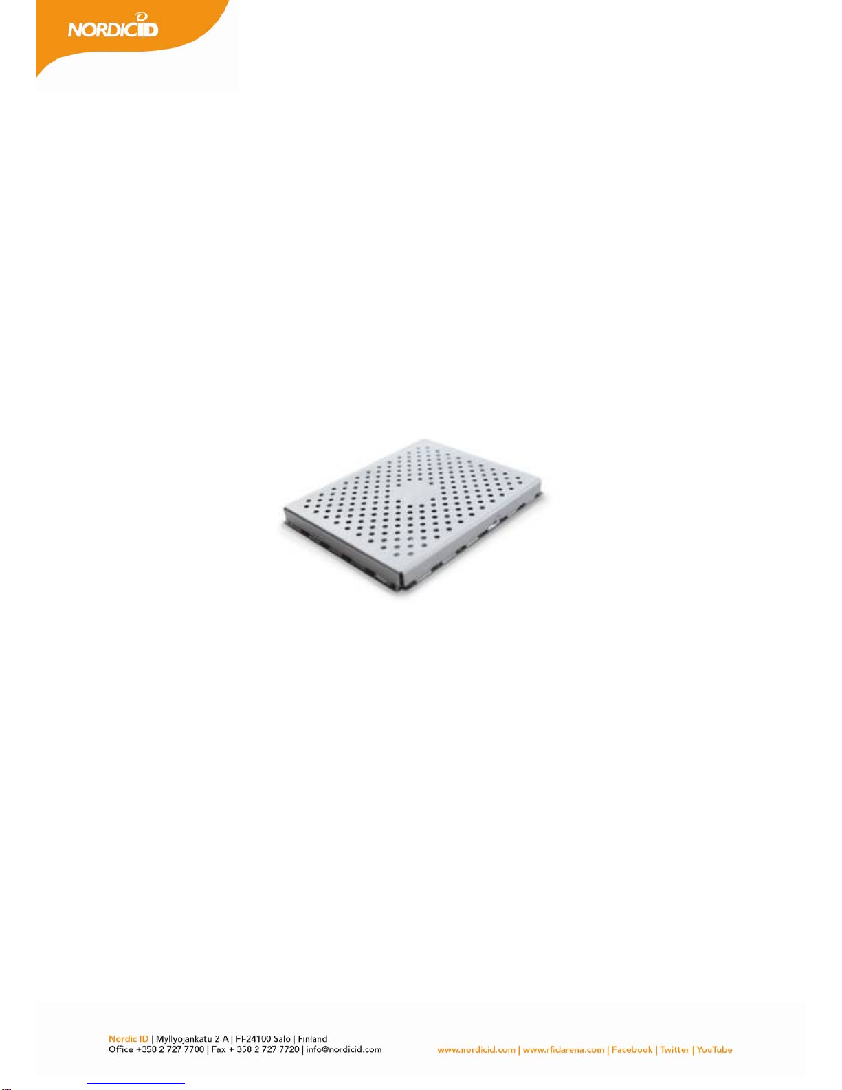
Nordic ID NUR-05WL2 User manual
2013‐09‐27
NUR‐05WL2ImplementationGuidev1.1
NUR‐05WL2IMPLEMENTATIONGUIDE
2013‐09‐27
NUR‐05WL2ImplementationGuidev1.1
Changehistory
VersionDateAuthorRemarks
0.12.1.2013ToniHeijariinitialversion
0.26.3.2013ToniHeijariminoradditions
0.34.4.2013ToniHeijarichangedsections1.3and4.1
1.012.6.2013ToniHeijarifirstreleasedversion
1.12.9.2013ToniHeijariChangedsection11.2and11.3

2013‐09‐27
NUR‐05WL2ImplementationGuidev1.1
Tableofcontents
1GENERAL DESCRIPTION ......................................................................................................................... 5
1.1 Block diagram.................................................................................................................................... 5
1.2 Key features ...................................................................................................................................... 5
1.3 Typical application schematics.......................................................................................................... 6
2ELECTRICALCHARACTERISTICS........................................................................................................................ 7
2.1 Absolute maximum ratings................................................................................................................ 7
2.2 DC characteristics ............................................................................................................................. 7
2.3 RF characteristics.............................................................................................................................. 7
2.4 Performance characteristics.............................................................................................................. 8
3PINASSIGNMENTS......................................................................................................................................... 9
3.1 Pin designation.................................................................................................................................. 9
3.2 Pin mapping....................................................................................................................................... 9
3.3 Signal description............................................................................................................................ 10
4OEMDESIGNCONSIDERATIONS.................................................................................................................... 12
4.1 RF output and antenna requirements ............................................................................................. 12
4.2 Power supply................................................................................................................................... 12
4.3 USB device port .............................................................................................................................. 13
5RFPARAMETERS.......................................................................................................................................... 14
5.1 TX level............................................................................................................................................ 14
5.2 Receiver sensitivity.......................................................................................................................... 14
5.3 Leakage cancellation....................................................................................................................... 14
5.4 Modulation....................................................................................................................................... 15
5.5 Link frequency................................................................................................................................. 15
5.6 RX encoding (Miller encoding)........................................................................................................ 15
5.7 Region............................................................................................................................................. 16
6READINGPARAMETERS................................................................................................................................18
6.1 Q-value............................................................................................................................................ 18
6.2 Session............................................................................................................................................ 18
6.3 Rounds............................................................................................................................................ 19
6.4 Selecting the right reading parameters........................................................................................... 19
7GPIOCONFIGURATIONS ............................................................................................................................... 21
7.1 Input / output.................................................................................................................................... 21
7.2 Predefined functions........................................................................................................................ 21
8DIAGNOSTICFUNCTIONS.............................................................................................................................. 24
8.1 Reflected power measurements...................................................................................................... 24

2013‐09‐27
NUR‐05WL2ImplementationGuidev1.1
8.2 Channel scanner............................................................................................................................. 24
8.3 Received signal strength (RSSI)..................................................................................................... 24
9DIMENSIONS ............................................................................................................................................... 25
9.1 Mechanical dimensions................................................................................................................... 25
9.2 Land pattern .................................................................................................................................... 27
9.3 Paste stencil.................................................................................................................................... 28
9.4 Packing tray dimensions ................................................................................................................. 29
10 SMTASSEMBLYPROCESSANDTHERMALPROCESSING ................................................................................... 31
10.1 Storage conditions........................................................................................................................... 31
10.2 Soldering process............................................................................................................................ 32
11 REGULATORYAGENCIESINFORMATION ........................................................................................................ 34
11.1 European Union and EFTA countries ............................................................................................. 34
User’sGuideRequirements ................................................................................................................ 34
LabelingRequirements....................................................................................................................... 37
ApprovedAntennas ........................................................................................................................... 37
11.2 FCC................................................................................................................................................. 38
User’sGuideRequirements ................................................................................................................ 39
LabelingRequirements....................................................................................................................... 39
ApprovedAntennas ........................................................................................................................... 40
11.3 Industry Canada.............................................................................................................................. 40
LabellingRequirementsfortheHostdevice ......................................................................................... 41
CertifiedAntennas ............................................................................................................................. 41
11.4 Industrie Canada............................................................................................................................. 42
Exigencesapplicablesauxappareilshôtes............................................................................................ 42
Typesd'antennesacceptables............................................................................................................. 42
2013‐09‐27
NUR‐05WL2ImplementationGuidev1.1
1GENERAL DESCRIPTION
NUR‐05WL2isanextgenerationcompactUHFRFIDreader/writermodule.Itiscompatiblewith
ISO18000‐6C(EPCC1G2)standard.ModulefulfillsETSI,FCCandICradioregulations.Itisalso
compatiblewithDRM(densereadermode)requirements.Maximumoutputpoweris+27dBmandit
canbeadjustedviaSWAPIwith1dBsteps.Maximumsensitivityis‐80dBm.
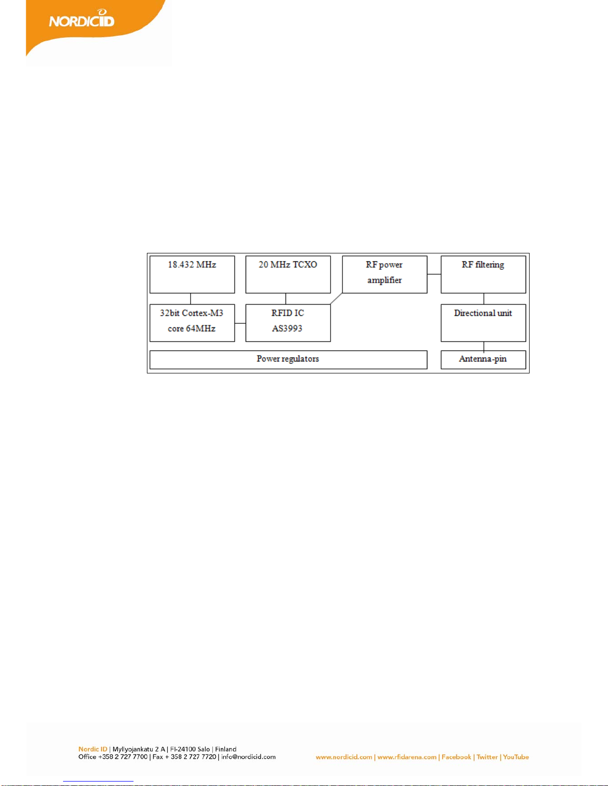
1.1 BLOCKDIAGRAM
1.2 KEYFEATURES
•SMTcompatiblemodulewithextremelysmallfootprint
•ISO18000‐6C(EPCC1G2)fullprotocolsupport+customcommands
•Lowpowerconsumptionwithhighnoiserejection
•DRMcompatible
•Highperformancewith+27dBmoutputpower,adjustableby1dBsteps
•ApprovedbyETSI,FCCandICtelecommunicationorganizations
•SelectableRFparameters;RXcoding,linkfrequencyandmodulation
•UARTandUSB2.0communication
•5programmableGPIOwitheventtrigger
•Autosensinginventoryparametersupport
•Increasedsensitivitywithautomaticleakagecancelation

2013‐09‐27
NUR‐05WL2ImplementationGuidev1.1
1.3 TYPICALAPPLICATIONSCHEMATICS
Typicalapplicationschematicincluding:USBconnectionwithESDprotectioncircuitry,2GPIOoutputs
forLEDindicators,GPIOtriggerinput,NUR‐05WL2moduleandMMCXantennaconnector.
Asimpleapplicationschematic.

2013‐09‐27
NUR‐05WL2ImplementationGuidev1.1
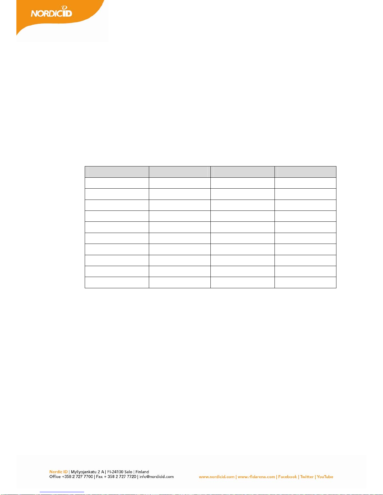
2ELECTRICALCHARACTERISTICS
2.1 ABSOLUTEMAXIMUMRATINGS
Violatingthesevaluesmaycausedamagetothemodule.Alsocorrectoperationisnotguaranteedif
operatingoutsidethesevalues.NUR‐05WL2isESDsensitivecomponentsoitmustbehandledwithcare.
AbsolutemaximumratingsValue
Operatingtemperature‐20°Cto+55°C
Storagetemperature(packageunopened)‐30°Cto+85°C
Supplyvoltageandenable+6.0V
GPIOpins+4.0V
Otherpins+4.0V
2.2 DCCHARACTERISTICS
Typicalvalues(VCC_3V6_IN=3.6V@+25°C)
SymbolParameterMinTypMaxUnits
Vext Supplyvoltage3.43.65.5V
Iext Supplycurrent‐0.8A1AmA
Isource GPIOsourcecurrent‐‐3mA
Isink GPIOsinkcurrent‐‐6mA
Vlow GPIOinputlow‐levelvoltage‐‐0.8V
Vhigh GPIOinputhigh‐levelvoltage 2.0‐ ‐ V
Ven Moduleenablevoltage1.2‐ SupplyV
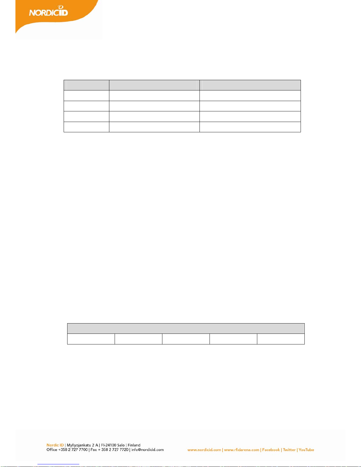
2.3 RFCHARACTERISTICS
Typicalvalues(VCC_3V6_IN=3.6V@+25°C)
SymbolParameterMinTypMaxUnits
Sens Receiversensitivity(datasensitivity
PER=0.1%/LBTsensitivity)‐ ‐ ‐70/‐80dBm
Pout Outputpower8±2‐ 27±2dBm
Padj Poweradjustmentstep‐1‐ dB
S11 VSWRrequirement‐‐1,5:1@50Ω
DrÆtReadertotagdatarates ‐ 40/80‐ kbps
DtÆrTagtoreaderdatarates2064320kbps

2013‐09‐27
NUR‐05WL2ImplementationGuidev1.1
2.4 PERFORMANCECHARACTERISTICS
Theperformanceofthereadermoduleishighlydependentonthetestenvironment,readerantennaand
tagperformance.Interferencesfromotherradiosourcesoperatinginthesamefrequencymaydecreasethe
performance.AlsothetagantennaandthetagICmayhavesignificanteffectonthevaluespresented
below.Alsoselectedradioandinventoryparametershavegotabiginfluencetoreadingperformance.
Typicalvalues(VCC_3V6_IN=3.6V@+25°C)
SymbolParameterMinTypMaxUnits
Rdist Typicalreadingdistancewith5dBiantenna‐ 5‐ m
Rrate Typicalreadingrate‐200‐ tags/s
Otemp Operationtemperature‐20‐ +55°C
Hrel Relativehumidity 10‐ 95%
2013‐09‐27
NUR‐05WL2ImplementationGuidev1.1
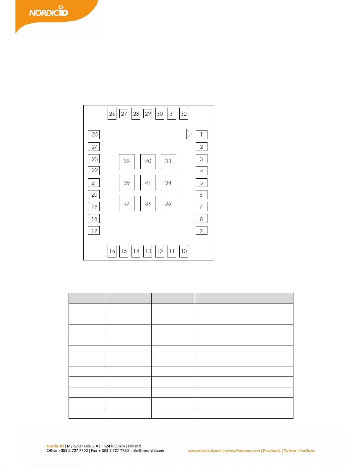
3PINASSIGNMENTS
3.1 PINDESIGNATION
Throughtopview.
3.2 PINMAPPING
PinnumberSignalnamePintypeDescription
1RFUBidirectionalRFU(donotconnect)
2GPIO_5Bidirectional3.3VGPIO
3GPIO_4Bidirectional3.3VGPIO
4GPIO_3Bidirectional3.3VGPIO
5GPIO_2Bidirectional3.3VGPIO
6GPIO_1Bidirectional3.3VGPIO
7ERASEInputDNU(donotuse)
8RXInputDatafromHosttoModule
9TXOutputDatafrommoduletoHost
10USB_DNBidirectionalUSB–(deviceport)
11USB_DPBidirectionalUSB+(deviceport)

2013‐09‐27
NUR‐05WL2ImplementationGuidev1.1
12USB_DETInputUsedonlyforUSBdetection
13VCC_3V3_OUTSupplyoutputDNU(onlyfortestingpurposes)
14MODULE_ENInputDrivinghighwillenablethemodule
15GNDSupplyinputGround
16NCNotconnectedinternallynotconnected
17VCC_3V6_INSupplyinputSupplyvoltageinput
18RFUBidirectionalRFU(donotconnect)
19RFUBidirectionalRFU(donotconnect)
20GNDSupplyinputGround
21GNDSupplyinputGround
22GNDSupplyinputGround
23GNDSupplyinputGround
24GNDSupplyinputGround
25GNDSupplyinputGround
26GNDSupplyinputGround
27RF_OUTBidirectional50ΩRFoutput/input
28GNDSupplyinputGround
29GND/RF_DIFBidirectionalRFU(donotconnect)
30GNDSupplyinputGround
31NCNotconnectedinternallynotconnected
32NCNotconnectedinternallynotconnected
33‐41GNDSupplyinputGround
3.3 SIGNALDESCRIPTION
Signalname:GND Pinnumber(s):15,20‐26,28,30,33‐41
Thesepinsareusedforgroundingandtoimprovethethermalperformance.Theyshouldbe
connectedtoHostboardGNDnet.
Signalname:GPIO_X Pinnumber(s):2‐6
ThesepinsareusedasgeneralpurposeIO.TheycanbeconfiguredviaSWAPIasinputoroutput
ports.IOvoltagelevelis3.3V.GPIOshavesourcecurrentcapabilityof3mAandsinkcurrentcapability
of6mA.
Signalname:ERASEPinnumber(s):7
Thispinisusedforproductiontestingpurposesonly.Shouldnotbeconnected.
Signalname:RX Pinnumber(s):8

2013‐09‐27
NUR‐05WL2ImplementationGuidev1.1
ThispinisusedformoduleUARTinputsignal.Logiclevelis3.3V.IfUARTisusedforcommunication
thepinshouldbeconnectedtotheHostMCUserialTXport.
Signalname:TX Pinnumber(s):9
ThispinisusedformoduleUARToutputsignal.Logiclevelis3.3V.IfUARTisusedforcommunication
thepinshouldbeconnectedtotheHostMCUserialRXport.
Signalname:USB_DN Pinnumber(s):10
ThispinisusedasUSB_D‐deviceport.ItisadvisedtouseexternalESDprotectioncomponentif
connectedtouseraccessibleUSBconnector.
Signalname:USB_DP Pinnumber(s):11
ThispinisusedasUSB_D+deviceport.ItisadvisedtouseexternalESDprotectioncomponentif
connectedtouseraccessibleUSBconnector.
Signalname:USB_DETPinnumber(s):12
ThispinisonlyusedforUSBconnectiondetection.ItisadvisedtouseexternalESDprotection
componentifconnectedtouseraccessibleUSBconnector.Currentisnotdrawnfromthisinputpin.
Signalname:VCC_3V3_OUT Pinnumber(s):13
Thispinisconnectedtointernalpowerregulatoroutput.Thepinisusedforproductiontestingandit
shouldnotbeused.
Signalname:MODULE_EN Pinnumber(s):14
DrivingthispintohighwillenabletheNUR‐05WL2module.Itisinternallyconnectedtoonboard
voltageregulator’senableinput.Thetriggerlevelis1.2Vandthereadermodulewillwakeupin50ms.
IftheexternalpowerswitchisusedtotoggleONandOFF,thispincanbeconnecteddirectlyto
VCC_3V6_IN.
Signalname:NC Pinnumber(s):16,31,32
Thesepinsareinternallynotconnected.
Signalname:VCC_3V6_IN Pinnumber(s):17
ThispinisusedforpowersupplyinputforNUR‐05Wmodule.Itisrecommendedtouse200µF(low
ESR)100nFand100pFcapacitorneartheVCC_3V6_INinputpintomaintainstableoperatingvoltage
forthereadermodule.
Signalname:RFU Pinnumber(s):1,18,19
Thesepinsarereservedforfutureuse.Donotconnectthesepins.
Signalname:GND/RF_DIF Pinnumber(s):29
ThispinisinternallyconnectedtoGND.ItisreservedforfutureuseassecondaryRFoutput.

2013‐09‐27
NUR‐05WL2ImplementationGuidev1.1
4OEMDESIGNCONSIDERATIONS
4.1 RFOUTPUTANDANTENNAREQUIREMENTS
TheRFoutput/inputimpedanceis50ΩsothetraceleavingfromtheRF_OUTpinshallbekeptinthatsame
impedanceleveltoavoidreflectionsandmismatchoftheRFsignal.Toprovideanappropriateimpedance
matchplacethematchingcomponentsclosetoRF_OUTpin.Belowthereisthecircuitdiagramthatshallbe
utilizedinthefine‐tuningoftheimpedancematchandintheadditionalfiltering.
FromtheRFIDreadermodule’spointofviewitisimportantthattheusedantennahasalowVSWRvalue.
TheVSWRshallbebetterthan1.5:1inordertoavoiddecreaseinthesensitivityperformanceofthe
receiverbecauseoftheTXpowerreflectingbackfromtheantenna.IntheNUR‐05WL2module,thereisalso
anautomaticleakagecancellationsystemthatdecreasestheeffectofthereflectedsignal,anditalso
improvestheisolationoftheRXsignalfromtheTXsignal.Theautomaticleakagecancellationcanbe
triggeredusingSWAPIcommand.Forfurtherinformationontheleakagecancellationseethesection5.3.
4.2 POWERSUPPLY
TheNUR‐05WL2hasinternallinearpowerregulatorsforgettingbetterpowersupplynoiserejection.
HoweveritisstillimportanttosupplylownoiseandstablepowertotheNUR‐05WL2module.Thevoltage
rippleshouldbekeptunder200mVppanditisrecommendedtoaddaminimumof200µFlowESR,100nF
and100pFcapacitorsnexttotheVCC_3V6_INpin.
VCC_3V3_OUTisinternalregulatoroutputanditisusedforproductiontestingpurposes.Thispinshould
notbeusedtopowerexternalcircuits.

2013‐09‐27
NUR‐05WL2ImplementationGuidev1.1
4.3 USBDEVICEPORT
USB_DP,USB_DNandUSB_DETpinsareusedtoprovide2.0compliantUSBdeviceport.Itmustbe
rememberedthatonlyonecommunicationmethodcanbeusedtocommunicatewiththeNUR‐05WL2
moduleatthetime.ConnectingtheUSBwillautomaticallypreventcommunicationviaserialport.Itis
advisedtouseexternalESDprotectioncomponentifconnectedtouseraccessibleUSBconnector.Belowis
thetypicalschematicsusedwithNUR‐05WL2module.
TypicalschematicsforUSBconnectionwithESDprotection.
Usedcomponents.
RefDescriptionManufacturerPartcode
U15ESDprotectionSTMicroelectronicsUSBLC6‐2SC6
L37CommonmodechokeMurataDLW21SN371SQ2L
2013‐09‐27
NUR‐05WL2ImplementationGuidev1.1
5RFPARAMETERS
5.1 TXLEVEL
Themaximumoutputpoweris+27dBm(500mW).Thepowercanbeadjustedby1dBsteps.Intotalthere
are19stepsmeaningtheminimumoutputpowervalueis+8dBmthatequalsto6mWofpower.When
usinghigheroutputpowerlevelstheantennasVSWRvaluebecomesmoreandmoreimportantfactor.High
outputpowercombinedtogetherwithantennawithpoorVSWRleadstoasituationwheresignificant
portionofthepowerisreflectedbacktothereceiver.
TXlevelPower:dBm/mWTXlevelPower:dBm/mW
027/5001017/50
126/3981116/40
225/3161215/32
324/2511314/25
423/2001413/20
522/1581512/16
621/1261611/13
720/1001710/10
819/79189/8
918/63198/6
5.2 RECEIVERSENSITIVITY
ThemaximumLBTsensitivityisof‐80dBm.Thereceivercanhandle+5dBmofpowerreflectingbackto
RF_OUTpinwithouthavingabigimpactontheperformance.Tolerancetoreflectingsignalcanbe
significantlyincreasedusingNUR‐05WL2leakagecancellationfunctionality.Thereceiverarchitectureuses
directconversionandithasanintegratedAGC(automaticgaincontroller).
5.3 LEAKAGECANCELLATION
Thedirectionalcoupleroftheinternalleakagecancellationcircuitryseparatestransmittedandreceived
signals.TuningthedirectionalcouplerincreasestheisolationbetweenTXandRXsignals.Youmaytunethe
directionalcouplerusingsoftware;thereisanAPIfunctionofitsownforthatpurpose.Noticethatthe

2013‐09‐27
NUR‐05WL2ImplementationGuidev1.1
tuningdoesnotmatchtheRF_OUTwithanantennasothegoodVSWR(returnloss)oftheantennaisan
essentialfactorofthegoodperformanceofthesystem.
5.4 MODULATION
ItispossibletouseASK(amplitudeshiftkeying)orPR‐ASK(phasereversedamplitudeshiftkeying)
modulation.TagsthatarecompliantwithISO18000‐6C(EPCC1G2)mustsupportbothofthese
modulations.ThePR‐ASKmodulationcantransferenergymoreefficientlytothetagbecauseRFenvelopeis
highmorethanitisusingASKmodulation.BydefaultthemodulationissettoPR‐ASK.
5.5 LINKFREQUENCY
Thelinkfrequencyaffectsthefrequencyoffsetoftagsreplyinrespecttoreader’scarrierwave.Forexample
whenusedlinkfrequencyis256kHz,tagwillreplyatthefrequencyofreadertransmissionfrequency±256
kHz.Theselectableparametersare160kHz,256kHzand320kHz.TagsthatarecompliantwithISO18000‐
6C(EPCC1G2)mustsupportalltheseparameters.Thelinkfrequencyalsoaffectstagtoreaderdatarate
whichiscalculatedbyformulabelow:
Tagtoreaderdatarate=(Linkfrequency/Millercoding)
Bydefaultthelinkfrequencyissetto256kHz.256kHzor320kHzsettingsmustbeusedwhenoperatingin
DRMmode.Itmustberememberedthatchangingtheseparametersmaycausereadertoviolateregionor
countryspecificradioregulations.Followingisaguidelineforhowtochoicerightsetting.Ifchannel
bandwidthis200kHzthan256kHzorlowerlinkfrequencyshouldbeused(forexampleinEU).When
operatinginaregionwhere500kHzchannelbandwidthisavailablealso320kHzlinkfrequencycanbe
used.
Spectralseparationcausedby256kHzlinkfrequencyandMillersub‐carrierencoding.
5.6 RXENCODING(MILLERENCODING)

2013‐09‐27
NUR‐05WL2ImplementationGuidev1.1
LikestatedabovetheMillersub‐carrierencodingschemeaffectsalsotagtoreaderdatarate.Inpracticethe
Millerencodingvalueaffectsthenumberofclockcyclesthattagusestomodulateonesymbol.Sowhen
usinghigherMillerencodingschemestagtoreaderdataratewillbeslowerbutatthesametimeitismore
robusttointerferences.Alsotagsresponsespectrumismoreconcentratedaroundthelinkfrequencywhen
usinghigherMillerschemes.Thisallowsthereceivertousenarrowerchannelfilters.Selectablevaluesare
M2,M4,M8orFM0.
ReceiverfiltersareoptimizedforM4andM8encodingschemes.WhenoperatingonDRMmodevalues4or
8shouldbeusedtooptimizetheperformance.BydefaultMiller4isused.Inadditiontomillerschemesalso
FM0encodingissupported.Inthiscaselinkfrequencydirectlydeterminesthetagtoreaderdatarate.
Tabledescribingdifferentdatarates.
Linkfrequency(kHz)RXencodingTagtoreaderdatarate(kbps)
160FM0160
160M280
160M440
160M820
256FM0256
256M2128
256M464
256M832
320FM0320
320M2160
320M480
320M840
5.7 REGION
TheNUR‐05WL2haspredefinedregionsettingsdefiningfrequencyandchannelsetsforoperatingunder
differentradioregulations.Globallytheregulationsvarydependingonthecountryorpartoftheworld.The
belowtableshowstheavailableoptionsfortheregionandtherespectivefrequencybandtheyuse.Note
thattheantennaalsoneedstobeworkingonthatsamefrequency.
Tableshowingpre‐programmedcountries/regions.
NumberCountry/regionFrequency/channelBW
0ETSI/Europe865.6–867.6MHz/200kHz
1FCC/North‐America902–928MHz/500kHz

2013‐09‐27
NUR‐05WL2ImplementationGuidev1.1
2People'sRepublicofChina920.5–924.5MHz/250kHz
3Malaysia919–923MHz/500kHz
4Brazil915–928MHz/500kHz
5Australia920–926MHz/500kHz
6NewZealand921.5–928MHz/500kHz
7Japan250mWLBT916.8–923.4MHz/200kHz
8Japan 916.8–920.4MHz/200kHz
9Custom840–960MHz
Ifyouwanttousecustomfrequenciesorhoptablesyouneedtofeedparameterdescribedbelow.
Tabledescribingcustomhoptableparameters.
ParameterValueDescription
Frequencyentry840000–960000[kHz]Definesthecenterfrequencyof
thefirsttransmitchannel.
Channelcount1‐100Definesthenumberoftransmit
channels
Channelspacing25*n[kHz]Definesthefrequencybetween
transmitchannels.
Channeltimeminimum100msDefinesthetimethatreadingis
ONatthesamechannel
Waittimemaximum1000msDefinesthetimethattransmitter
issilentbetweenfrequencyhops
Tari1=12.5us2=25usDefinestheTarivalue
LF160000,256000or
320000
Definesthemaximumlink
frequencythatisused

2013‐09‐27
NUR‐05WL2ImplementationGuidev1.1
6READINGPARAMETERS
6.1 Q‐VALUE
TheQ‐valuedefinestheamountofopenresponseslotsthattagscanuseperoneinventoryround.Number
ofslotscanbecalculatedbyformula2Q.Itisadvisedtousetwiceasmuchslotscomparedtoamountoftags
thatyouhaveinyourreadersreadingfieldsimultaneously.Selectablevaluesare0–15andvalue0means
automaticQ‐valueadjustment.WhenQ=0isusedreaderwillautomaticallyincreasetheQ‐valuewhenlots
ofcollisionsarenoticedanddecreasedthevaluewhenthereareonlyfewcollisions.BydefaulttheQ‐value
issetto0.
TableindicatingtherelationbetweentheQ‐valueandthenumberofopenslotsperround.
Q‐valueslotsQ‐valueslots
0automatic8256
129512
24101024
38112048
416124096
532138192
6641416384
7128 1532768
6.2 SESSION
Therearefoursessionoptionswhichyoucanusewheninitializinginventoryround.Everysessionhastwo
targetstatesAandB.BydefaultGen2tagsareatstateAiftaghasnotbeenreadrecently.Whentagisread
itflipstostateBanddoesn’treplytoreadersquery.Thetablebelowdescribesthepersistenceoftag’sstate
machinewhenusingdifferentsessionvalues.Forexamplewhenusingsession0thetagwillcomebackto
stateAimmediatelywhentagpowerislost.Usuallytaglosesthepowerwhenreaderstopstheinventory
roundorchancesthechannel.PersistencewhentagpowerisONisnotdefinedbytheISO18000‐6Cwhen
usingsessionsettingsS0,S2andS3.Withsession1thetagwillkeepitstateover500msbutlessthan5s.
Withsessionvalues2and3tagswillkeepitstatesover2swhentagpowerislost.Timecanvarydepending
whattagICisused.
2013‐09‐27
NUR‐05WL2ImplementationGuidev1.1
Tableindicatingpersistencecharacteristicsofgen2tags.
FlagPersistence:tagpowerONPersistence:tagpowerOFF
S0indefinitenone
S1500ms<t<5s500ms<t<5s
S2indefinitet>2s
S3indefinitet>2s
BychangingthetargetsettingfromAtargettoBtargetreaderisabletoreadalsotagsthathasflippedits
statetoBstate.ThiswouldhappeniftagswouldhavebeenreadrecentlyusingSession12or3.NUR‐05WL2
modulealsosupportsdualtargetmode.Inthatmodereaderwillchangethetargetmodebetweeninventory
rounds.BydefaulttargetmodeAisused.
6.3 ROUNDS
Theroundssettingdefineshowmanyqueryroundsisdoneinsideoneinventoryround.Afterevery
inventoryroundthereaderwillsenddatatotheHost.Selectablevaluesare0–10.Zeromeaningautomatic
roundsadjustment.Theautomaticadjustmentdecidesaftereveryqueryroundwhetheranotherroundis
necessarybasedonthenumberofdatacollisions.Bydefaultroundssettingissetto0.Thissettingcanhelp
thereadertofindallthetagsthatareinthereadersreadingfieldwhenusingsession0.Becausetagsthat
arefoundinqueryround1doesn’treplayinthefollowingqueryrounds.Whenusingsession1/2/3this
doesnotmakeanysignificantdifferencebecausetagsthatarereadarequietanyway.
Tabledescribingrelationbetweeninventoryroundandqueryround.
Inventoryround
Round1Round2round3…Round10
6.4 SELECTINGTHERIGHTREADINGPARAMETERS
Oneapproachistotesthowmanytagsareinthereadersreadingfieldsimultaneously.Keepthereaderstill
atthepositionthatisasclosetorealreadingenvironmentaspossibleandseehowmanytagsarefound.
Basedonthatamountchooseyouropenslotnumbertobe1.5–2timeslarger(refertothesection6.1).If
readerwillfacemanydifferenttagpopulationsauto‐Qsettingwillbeagoodchoice.

2013‐09‐27
NUR‐05WL2ImplementationGuidev1.1
BesidesQ‐valueoneimportantparameterissession.Ingeneralitcouldbestatedthatifthesizeoftag
populationismeasuredinthousandsratherthaninhundredsitiswisetousesessions2or3.Becausethen
everytagwillbereadonlyonceandthatmakeslargetagpopulationmuchfasterandeasiertoread.When
usingsession2or3itisadvisedtouseMiller8encodingschemetoavoiddatatransfererrorsasmuchas
possible.Rounds1settingisalsoadvisedtobeusedwithsession1or2or3.Withsession0itmightbe
usefultousehigherroundsvaluethan1tobeabletofindalltheindividualtags.Bydefaultautomatic(0)
roundssettingisused.
Othersettingslikemodulation,linkfrequencyandRX‐encodinghasaminorimpacttothereadingspeedof
thereader.Whenoperatinginoptimalenvironmentfollowingwillapply:
RXencoding:FM0isfastestbutquitesensitivetointerferences/M8slowestbutveryrobust
Modulation:NoeffecttospeedbutPR‐ASKhasbetterrangewithsometags
Linkfrequency:320kHzisthefastest/160kHzistheslowest
Guidelinesettingstobeusedwithdifferenttagpopulations.
SettingsTagpopulationSimultaneouslyinthefield
Session0,autoQ,autoRounds 1–1001–100
Session1,autoQ,Rounds1100–1000under500
Session2/3,autoQ,Rounds1100–1000over500
Session2/3,autoQ,Rounds1over1000over500
Table of contents
Other Nordic ID Other manuals


