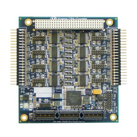
Noyes PERICOM PI5USB1458 User manual

Pericom Company Confidential
Pericom Semiconductor Corp.
www.pericom.com
Page 1 of 1 4/29/2013
PI5USB1458 / PI5USB1458A
PI5USB1458/PI5USB1458A EVB Rev.A User Manual
by Noyes Mok
Introduction
Pericom’s PI5USB1458 and PI5USB1458A are the USB sleep & charge switch with Vbus switch control function
which provides multimode supports auto-detection and auto-switching between modes by detecting correctly plugged
in device.
The PI5USB1458 series evaluation board (EVB) is designed to demonstrate the benefits, performance and key
features of PI5USB1458 and PI5USB1458A. This user manual describes the usage of this EVB and it will be divided
into following sections:
•Overview
•Quick start
•Board Design information
PI5USB1458/PI5USB1458A EVB Schematic
PCB Layout
PCB Layout Reference
BOM List
Overview
Figure 1(a) & 1(b) are the block diagrams of Pericom PI5USB1458/PI5USB1458A EVB and Figures 2(a) & (b) are
the top and bottom view of EVB board. There is an USB plug connectors (J2) which is used to connect PC’s USB
port and the USB receptacle connector (J1) is used to connect mobile devices. An external Vbus switch
PI5PD2068/PI5PD2069 is assembled on EVB which is controlled by the INT# / INT pin of
PI5USB1458/PI5USB1458A. The MODE setting in SW1 is used to select the normal USB operation and simulate
the Standby or Sleep mode (S3/ S4) of the PC. The LED D1 is used to show whether the circuit is over-current or
over-temperature. PI5USB1458/PI5USB1458A operation required +5V which was supplied by the PC through the
USB connector (J2) or external power supply +5V through JP2 & JP3.
Figure 1a, block diagram of PI5USB1458 EVB
2
1
PI5USB1458
J1
USB
Receptacle
USB
Plug
INPUT
J
2
OUTPUT
Switch for Mo e
select
PI5PD
2068
EN#
SB#
SW1
INT#
D1

Pericom Company Confidential
Pericom Semiconductor Corp.
www.pericom.com
Page 2 of 2 4/29/2013
Figure 1b, block diagram of PI5USB1458A EVB
Figure 2(a), top view of PI5USB1458/PI5USB1458A EVB Figure 2(b), bottom view of PI5USB1458/PI5USB1458A EVB
2
1
PI5USB1458A
J1
1
USB
Receptacle
USB
Plug
INPUT
J2
OUTPUT
Switch for Mo e
select
PI5PD2069
EN
SB#
SW1
INT
D1

Pericom Company Confidential
Pericom Semiconductor Corp.
www.pericom.com
Page 3 of 3 4/29/2013
Quick Start
To start-up the PI5USB1458/ PI5USB1458A EVB, complete the following steps:
1. Check the head pin status and SW1 setting follow Table 1
2. EVB USB connector J2 plugged into PC’s USB connector.
3. For Normal USB operation, SW1 switch to RIGHT side (SB# = 1 - Normal USB mode)
For Auto sleep and charge mode on mobile device charging, SW1 switch to LEFT side (SB# = 0 - Auto sleep and
charge mode)
4. Power up the PC
5. Plug the mobile device into EVB USB connector J1
Header pin is set as defaulted on EVB.
He
ader
pin #
Pin
name
for
PI5USB1458
Pin name for
PI5USB1458A Switch status Remark
JP1 VBUS_OUT VBUS_OUT Short
JP4 VDD VDD Short EVB power up by the PC
JP5 SEL SEL Short SEL = H
SW1 Configure
mode
Configure
mode
LEFT →SB#=0 (Auto sleep and
charge)
-Auto sleep and charge mode was set as default on EVB
Table 1, Header pin settings for EVB (header pins location refers to Figure 4)
Figure 3, Connection of PI5USB1458 / PI5USB1458A EVB
PC
Mobile device
EVB plug-into
PC USB port
PI5USB145
8
/
PI5USB1458A
EVB
Auto
Sleep &
Charge
Normal
USB
mode
Auto
Sleep &
Charge

Pericom Company Confidential
Pericom Semiconductor Corp.
www.pericom.com
Page 4 of 4 4/29/2013
Detail Description
The functionality of header pins, switch are detail described in this section.
Functionality of Header Pins & Banana Jack
Header
Pin
Description
Remark
PI5USB1458
PI5USB1458A
JP1
Pin 1 = PI5PD2068 output
Pin 2 = Vbus pin of USB
receptacle connector
Pin 1 = PI5PD2069 output
Pin 2 = Vbus pin of USB
receptacle connector
Short = connect the +5V output to
USB receptacle connector
JP4 Pin 1 = Vbus from USB plug
Pin 2 = VDD of PI5USB1458
Pin 1 = Vbus from USB plug
Pin 2 = VDD of PI5USB1458A
Short =EVB power up by Vbus of
USB plug
Open = EVB need to power up by
external power supply
JP5 Pin 1 = 10kohm to +5V
Pin 2 = SEL of PI5USB1458
Pin 1 = 10kohm to +5V
Pin 2 = SEL of PI5USB1458A
Short →SEL = high
Open →SEL = Low
Banana
Jack PI5USB1458 PI5USB1458A Remark
JP2 GND GND If use external power support, JP4
must be Open
JP3 +5V from external power
support
+5V from external power
support
Functionality of Switches
Switch
Pin on
PI5USB1458/
PI5USB1458A
Description
SW1 SB#
Configure Mode,
0 (LEFT side) = Sleep and charge mode,
1 (RIGHT side) = Normal USB mode
Switches and header pin Setting
SB#
SEL Feature
SW1
JP5
0 0 Auto Sleep & Charge - with keyboard/mouse pass through
1
1 0
S
0 chargin
g with SDP only
1
S
0 charging with CDP / SDP (depends on external device)
LEFT side =
Sleep and
charge mode
RIGHT side =
USB mode

Pericom Company Confidential
Pericom Semiconductor Corp.
www.pericom.com
Page 5 of 5 4/29/2013
Board Design Information:
PI5USB1458/PI5USB1458A EVB Schematic
U2
PI5USB1458/PI5USB1458AZAE@TDFN8
INT/INT#
1
D-
2
D+
3
SEL
4VDD 5
Y+ 6
Y- 7
SB# 8
HGND 9
C5
0.1u_0402
+5V
J2
CON_USB2.0_TA_Plug
VBUS
1
D-
2
D+
3
GND
4
Shell
5
J1
CON_USB2.0_TA_Rec
VBUS 1
D- 2
D+ 3
GND 4
Shell
5Shell 6
SB#1
2
1
3
VBUS_OUT
JP1
1
2
R4
10k
R5
10k
+5V
JP5
1
2
+5V
R6
10k
JP3
+5V
1
JP2
GND
1
C1
4.7uF
C4
22uF
C3
0.1uF
VBUS_OUT
JP4
1
2
+5V
+5V
+5V
D1
LED_R
12
+5V
R1 560
U1
PI5PD2069 / PI5PD2068@SOIC8
GND
1
IN
2
IN
3
EN
4OC# 5
OUT 6
OUT 7
OUT 8
PAD_GND 9
C2
0.1uF
+5V VBUS
R3
10k
R2
10k
For
PI5USB1458A, put
10k on R2 and R3
floating
For PI5USB
145
8
,
put 10k on R3 and
R2
floating

Pericom Company Confidential
Pericom Semiconductor Corp.
www.pericom.com
Page 6 of 6 4/29/2013
PCB Layout
Figure 4, Top view of PI5USB1458/PI5USB1458A EVB Layout
Figure 5, Bottom view of PI5USB1458/PI5USB1458A EVB Layout
J
1
USB
Receptacle
J
2
USB Plug
SW1
JP4
J
1
USB
Receptacle
J
2
USB Plug
JP5
VBUS_IN
GND
JP1
VBUS_IN
GND

Pericom Company Confidential
Pericom Semiconductor Corp.
www.pericom.com
Page 7 of 7 4/29/2013
PCB Layout Requirements
a. Stack Up:
Layer # Plane Material Type Thickness (mil)
Solder Mask
0.4
Layer 1 Signal 1.2
Prepreg FR4 1080
FR4 2216 7.3
Layer 2 GND 1.2
Core 44
Layer 3 Power 1.2
Prepreg FR4 2216
FR4 1080 7.3
Layer 4 Signal 1.2
Solder Mask 0.4
b. Isolation Spacing = 30 mil
c. Width & Spacing (W/S) of 90ΩDifferential Trace = 11 / 10 / 11 mil
BOM List
Item Quantity Reference Description
1 1 C1 4.7uF Capacitor
2 3 C2, C3, C5 0.1uF Capacitor
3 1 C4 22uF Capacitor
4 1 D1 Red LED
5 3 JP1, JP4, JP5 2X1 Header Pin
6 2 JP2, JP3 Banana Jack
7 1 J1 USB 2.0 Receptacle connector
8 1 J2 USB 2.0 Plug connector
9 1 R1 560ΩResistor
10 6 R2, R3, R4, R5, R6, R14 10kΩResistor
11 1 SW1 SPDT switch
12 1 U1 PI5PD2068 / PI5PD2069
13 1 U2 PI5USB1458 / PI5USB1458A
This manual suits for next models
1
Table of contents