nvent Schroff 21265-010 User manual

Embedded COM System
User‘s Manual
Product Number:
21265-010/020/030
Doc-No: 63972-366_R1.5 April 2018

Impressum:
Schroff GmbH
Langenalber Str. 96 - 100
75334 Straubenhardt, Germany
The details in this manual have been carefully compiled and
checked - supported by certified Quality Management System
to EN ISO 9001/2000
The company cannot accept any liability for errors or misprints.
The company reserves the right to amendments of technical
specifications due to further development and improvement of
products.
Copyright2018
All rights and technical modifications reserved.
R1.5 April 2018 rebranded

21265-010/020/030
I R1.5, April 2018
Table of Contents
1 Safety .................................................................................................................................... 1
1.1 Safety Symbols used in this document ........................................................................... 1
1.2 General Safety Precautions................................................................................................ 1
1.3 References and Architecture Specifications................................................................... 1
2 Introduction.......................................................................................................................... 2
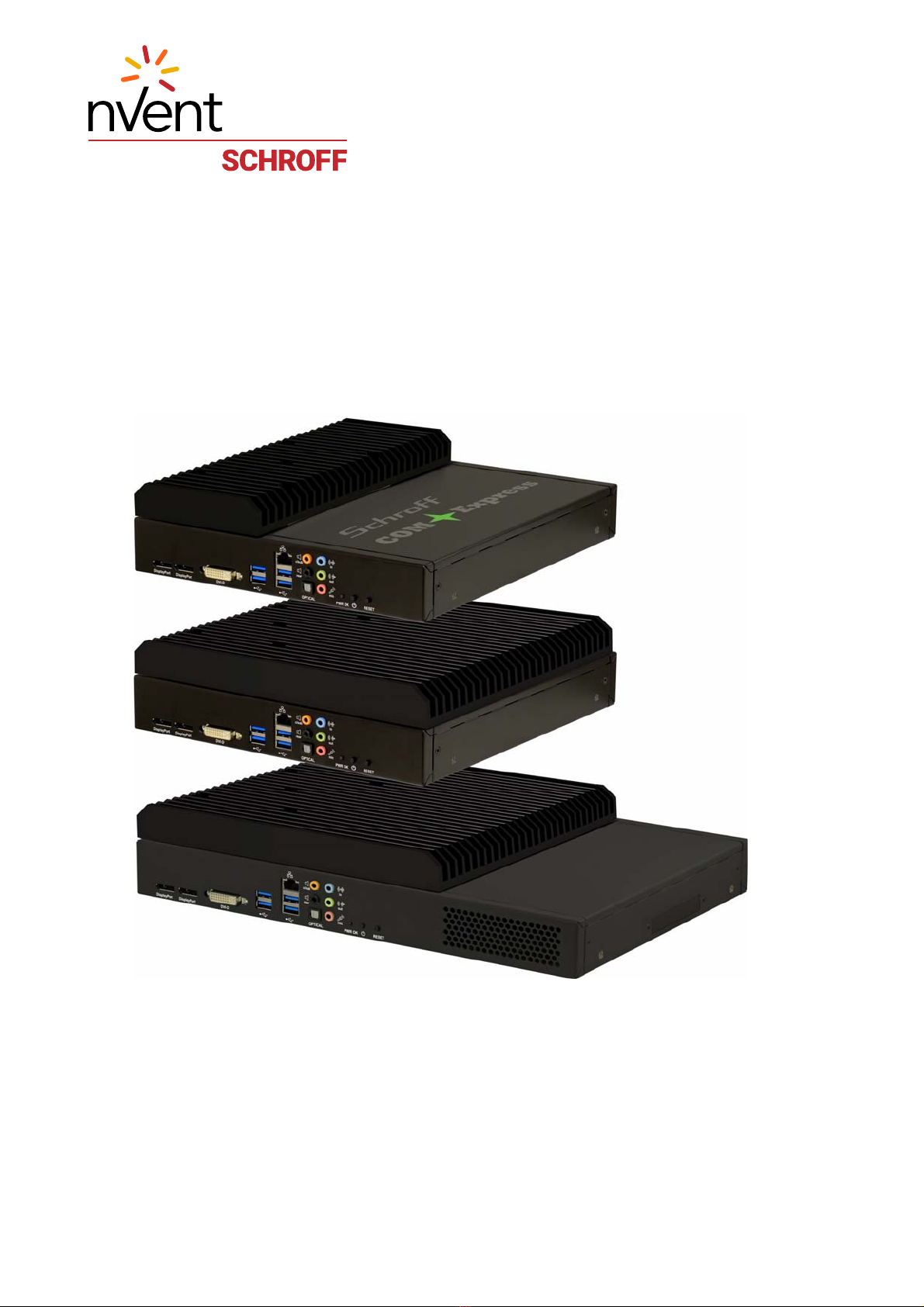
2.1 Schroff Embedded COM System ...................................................................................... 2
2.2 System Overview.................................................................................................................. 3
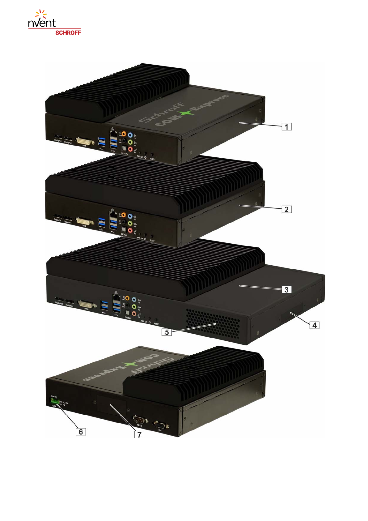
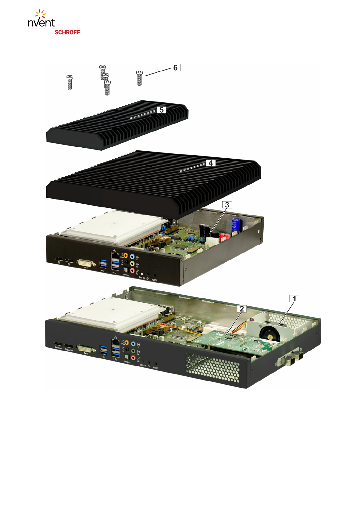
2.3 Disassemble the Case......................................................................................................... 7
2.4 Schroff Carrier Board........................................................................................................... 8
2.5 COM Carrier........................................................................................................................... 9
2.6 Fixing Post Layout.............................................................................................................. 10
2.7 COM Carrier Connector and Jumper Overview............................................................ 11
2.8 Jumper Settings Overview ............................................................................................... 12
2.9 Connector Overview .......................................................................................................... 13
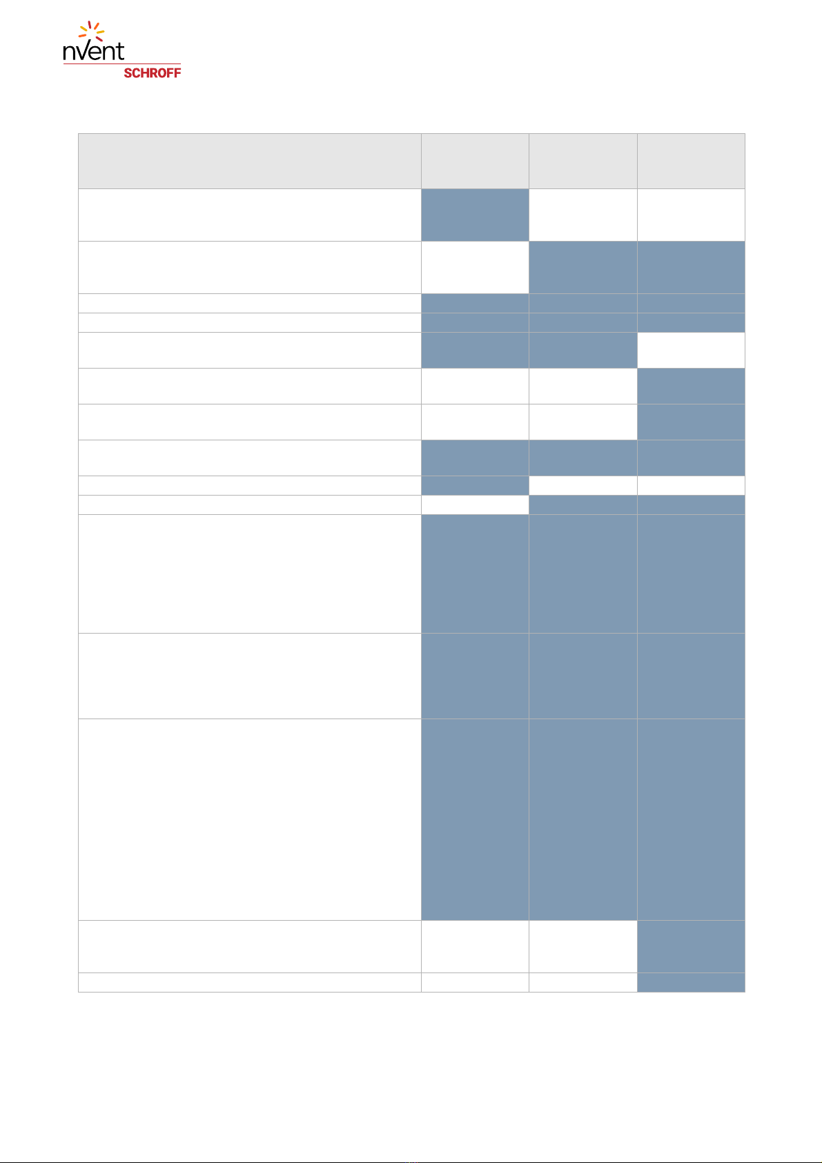
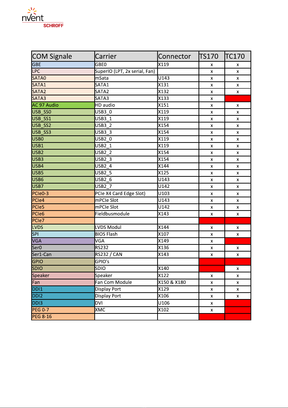
2.10 Signal Routing..................................................................................................................... 14
3 Power .................................................................................................................................. 15
3.1 Power Input ......................................................................................................................... 15
3.2 Power Connectors and Jumpers .................................................................................... 16
4 Interfaces ........................................................................................................................... 17
4.1 LPC Super I/O Controller................................................................................................... 17
4.2 Serial Interfaces.................................................................................................................. 17
4.3 Parallel Interface................................................................................................................. 18
4.4 I2C-Bus, SMBus and CAN Interfaces ............................................................................. 18
4.5 SPI Flash EEPROM............................................................................................................. 19
4.6 USB ....................................................................................................................................... 20
4.7 Ethernet................................................................................................................................ 20
4.8 SATA ..................................................................................................................................... 20
4.9 PCI Express ......................................................................................................................... 21
4.10 MiniPCIe............................................................................................................................... 21
4.11 XMC ...................................................................................................................................... 22
4.12 XMC I/O Plug-on Module .................................................................................................. 23
4.13 Fieldbus Interface............................................................................................................... 24
4.14 LVDS Interface.................................................................................................................... 25
4.15 Prototype Interface ............................................................................................................ 26
4.16 Fan Control.......................................................................................................................... 27
4.17 Audio Interfaces ................................................................................................................. 28
4.18 Video Interfaces ................................................................................................................. 29
5 Technical Data................................................................................................................... 30

21265-010/020/030
II R1.5, April 2018

21265-010/020/030
Safety 1 R1.5, April 2018
1 Safety
The intended audience of this User’s Manual is system integrators and hardware/software
engineers.
1.1 Safety Symbols used in this document
1.2 General Safety Precautions
• Service personnel must know the necessary electrical safety, wiring and connection
practices for installing this equipment.
• Install this equipment only in compliance with local and national electrical codes.
1.3 References and Architecture Specifications
• PICMG® COM Express Module™ Base Specification
(www.pigmg.org)
• PICMG® COM Express® Carrier Design Guide
(www.pigmg.org)
Caution!
This is the user caution symbol. It indicates a condition where damage of the equipment or
injury of the service personnel could occur. To reduce the risk of damage or injury, follow all
steps or procedures as instructed.
Danger of electrostatic discharge!
The COM Carrier contains static sensitive devices. To prevent static damage you must wear
an ESD wrist strap.

21265-010/020/030
Introduction 2 R1.5, April 2018
2 Introduction
COM Express® is a PICMG® standard that describes a COM (Computer-On-Module) and the
supporting Carrier Board.
• The COM contains the processor, RAM, and I/O ICs.
• The Carrier Board provides power to the COM, additional I/O ICs, and all of the
I/O connections.
Together the COM and Carrier Board make a bootable computer.
The electrical and mechanical interface between the COM and Carrier Board has several
“Type” definitions. The user can select a COM and Carrier Board with an interface Type that
matches their requirements.
2.1 Schroff Embedded COM System
The Schroff Embedded COM Systems combine Schroff COM Carrier boards and COM Express
Type 6 modules in an Interscale case with convection cooling including a power board with
18 VDC - 26,4 VDC input voltage.
•21265-010: Embedded COM System with congatec conga-TC170/3955U (045203)
COM Express Type 6 Compact module with Intel® Celeron® 3955U dual core processor
with 2.0 GHz, 2 MB L2 cache and 2133 MT/s dual channel DDR4 memory interface
•21265-020: Embedded COM System with congatec conga-TS170/i7-6820EQ (045900)
COM Express Type 6 Basic module with Intel® Core™ i7-6820EQ quad core processor with
2.8 GHz up to 3.5 GHz, 8MB L2 cache, GT2 graphics and 2133 MT/s dual channel DDR4
memory interface, Chipset QM170
•21265-030: Embedded COM Lab System with slots/connectors for prototype and XMC
modules and congatec conga-TS170/i7-6820EQ (045900) COM Express Type 6 Basic
module with Intel® Core™ i7-6820EQ quad core processor with 2.8 GHz up to 3.5 GHz, 8
MB L2 cache, GT2 graphics and 2133 MT/s dual channel DDR4 memory interface,
Chipset QM170
All systems come with a power board generating the COM Carrier supply voltages
(1.5 V, 3.3 V, 5 V, 12 V) from the system input voltage (18 - 26,4 VDC)

21265-010/020/030
Introduction 3 R1.5, April 2018
2.2 System Overview
* Interfaces supported by the pre-assembled COM Modules see Figure 1
21265-010
Embedded COM
System
21265-020
Embedded COM
System
21265-030
Embedded COM
Lab System
Type 6 Compact module with Intel® Celeron® 3955U dual
core processor;
4 GB DDR4-SODIMM-2400
X
Type 6 Basic module with Intel® Core™ i7-6820EQ quad core
processor;
8 GB DDR4-SODIMM-2400
X X
SSD 120 GB SATA XXX
Power/Data Cable for Hard Disk XXX
COM Carrier (partly assembled w/o XMC and Prototype con-
nectors)
X X
COM Carrier (fully equipped with XMC and Prototype con-
nectors)
X
Slot for an optional XMC Module at the right side covered
with a dummy panel
X
Slot for an optional Fieldbus Module at the rear side covered
with a dummy panel
XXX
Heatsink medium power X
Heatsink high power X X
Front Panel Connectors:*
DVI
2x Display Port
4x USB 3.0
S/PDIF Optical
HD audio I/O
Gigabit Ethernet UTP
XXX
Rear Panel Connectors:*
15-pin VGA
Serial Port (DSUB9)
Power
XXX
Connectors/slots on PCB:*
2x MiniPCI Express
Fieldbus Module connector
LVDS Module connector
PCI Express slot with 4x PCIe
3x SATA ports
2x Micro SIMM
1 serial port
Parallel printer port
1x MicroSD
Speaker
Interface for POST code display
XXX
XMC Module Connector
XMC I/O Plug-on Module Connector
Prototype Module Connector
X
Fan for XMC Module X

21265-010/020/030
Introduction 4 R1.5, April 2018
Figure 1: Interfaces supported by the COM Modules

21265-010/020/030
Introduction 5 R1.5, April 2018
Figure 2: Embedded COM Systems
1Embedded COM System (Celeron) 5Air inlet
2Embedded COM System (i7) 6Power input
3Embedded COM Lab System 7Slot for optional Fieldbus Module
4Slot for XMC Module

21265-010/020/030
Introduction 6 R1.5, April 2018
Figure 3: Embedded COM Systems Overview
1Fan for XMC Module (Optional) 4Heatsink (Large for i7 COM Modules)
2XMC Module (Example, not scope of delivery) 5Heatsink (Small fpr Celeron COM Modules)
3Power Module 6Heatsink (Fixing Screws)

21265-010/020/030
Introduction 7 R1.5, April 2018
2.3 Disassemble the Case
Figure 4: Disassemble the Case
Disassemble the case:
• Remove the 2 screws (1)
• Pull the frontpanel (2) forwards
• Remove the screws (3)
• Remove the heatsink (4)
• Pull the top cover (5) upwards

21265-010/020/030
Introduction 8 R1.5, April 2018
2.4 Schroff Carrier Board
The Schroff COMET6 Carrier Board supports the Type-6 interface definition described in the
PICMG COM Express Module Base Specification, and can be used with any Type-6 COM.
This allows the user to select a Type-6 COM with as much or as little processing power as
needed for the specific application. The COMET6 Carrier Board can be used as is in an
application, or as the basis for a custom application specific Carrier Board design.
Interfaces:
• 2x MiniPCI Express modules with USB, one with mSATA
• Fieldbus Module for developing interfaces such as CAN or second ethernet
• LVDS Display Module
• XMC Module
• XMC I/O Plug-on Module
• PCI Express slot with PCIe x4
•3xSATAports
• Gigabit Ethernet UTP
• 3x serial ports
• Parallel printer port
•MicroSD
• 15-pin VGA
•DVI
•2xDisplayPort
• 1x USB 2.0 and 4x USB 3.0
•S/PDIFOptical
• HD audio I/O
•Speaker
• Interface for POST code display
• The COMET6 Carrier Board also includes a socket for a SPI flash device that can be used
for BIOS expansion, and a 32 kbyte I2C SEEPROM
The Schroff COMET6 Carrier Board is designed for Compact- or Basic-sized
COM Modules and supports the Type-6 interface.

21265-010/020/030
Introduction 9 R1.5, April 2018
2.5 COM Carrier
Figure 5: COM Carrier with Power Module

21265-010/020/030
Introduction 10 R1.5, April 2018
2.6 Fixing Post Layout
When the factory-installed COM Module is replaced by an Module with a different form
factor, some fixing posts mus be removed or added.
Figure 6: Fixing Post Layout

21265-010/020/030
Introduction 11 R1.5, April 2018
2.7 COM Carrier Connector and Jumper Overview
Figure 7: COM Carrier Connector and Jumper Overview
Blue: Jumper
Red: Connector

21265-010/020/030
Introduction 12 R1.5, April 2018
2.8 Jumper Settings Overview
Jumper Settings
X110 Vcc to USB 1-2: Vcc to USB in Suspend State 4 (COM Express Module)
X111 Incorrect COM Module Type will dis-
able Vcc
1-2: Incorrect COM Module Type will disable Vcc (COM Express Module)
2-3: Incorrect COM Module Type will not disable Vcc
X113 SDcard Selection 1-2: AEN# MicroSD in Socket X140
2-3: BEN# GPIO on Prototype Module
X115 BIOS Selection Strap 1-2: Connects BIOS_DIS0# to ground
X116 BIOS Selection Strap 1-2: Connects BIOS_DIS1# to ground
X117 SPI Power Selection 1-2: Connects SPI_POWER to pin 5 of X109
X120 XMC Power Selection 1-2: connects VCC_12V to XMC
2-3 or no jumper connects VCC_5V0 to XMC
X124 Serial port on DB9 connector X136 1-2 & 7-8 for Serial Port B on Super I/O
3-4 & 5-6 for Serial Port 0 on COM Module
X138 Disable Vcc in a Suspend State 1-2: Always Enable Vcc
3-4: Disable Vcc in Suspend State 3
5-6: Disable Vcc in Suspend State 4
7-8: Disable Vcc in Suspend State 5
X161 Super I/O Oscillator frequency 1-2: Super I/O Oscillator frequency = 48 MHz
2-3: Super I/O Oscillator frequency = 24 MHz

21265-010/020/030
Introduction 13 R1.5, April 2018
2.9 Connector Overview
*Only Fan Power, Tacho and PWM not supported by the BIOS
Connector
U103 PCIe [0-3] x4 Card Edge
U142 Mini PCIe, 52-pin, PCIe #5, USB2 #7, Micro SIMM socket on X126
U143 Mini PCIe, 52-pin, PCIe #4/SATA #0, USB2 #6, Micro SIMM socket on X127
X100 XMC J16
X101 XMC I/O Plug-on Module
X102 XMC J15
X103 Power for XMC I/O Plug-on Module
X104 POST Code Module
X105 Serial A from the Super I/O
X106 I²C-Bus, SMBus, CAN Bus
X107 SPI Flash Device socket
X108 Display Port
X109 SPI Programming Port
X112 4-Wire Fan with control from SuperI/O (LPC)*
X118 3-Wire Fan with control from the COM Module
X119 USB0, USB1, and Ethernet
X121 Connector NTC Temperature Sensor from Super IO
X122 Speaker
X125 USB #5 Host
X126 Micro SIMM #1 socket for Mini PCIe on U142
X127 Micro SIMM #2 socket for Mini PCIe on U143
X128 Type-6 COM Express Module
X129 Display Port
X130 Parallel Printer Port from Super I/O
X131 SATA Port #1
X132 SATA Port #2
X133 SATA Port #3
X134 Ground for test probe
X135 Input ext. -12 V for XMC J15
X136 DB-9 Serial
X140 MicroSD Socket
X142 Disk Drive Power
X143 Fieldbus Module
X144 LVDS Module
X145 Prototype Module
X146 Power Board
X148 XMC Module JTAG
X149 VGA
X150 4-Wire Fan with control from the COM Module
X151 HD Audio
X153 DVI
X154 USB #2 and #3
X156 Current measurement shunt for +5.0 V Standby on COM Module
X157 Current measurement shunt for +12.0 V on COM Module
X158 Current measurement shunt for +3.3 V Standby
X159 Current measurement shunt for +5.0 V Standby
X160 Current measurement shunt for +12.0 V from PSU

21265-010/020/030
Introduction 14 R1.5, April 2018
2.10 Signal Routing
Figure 8: Signal Routing

21265-010/020/030
Power 15 R1.5, April 2018
3 Power
3.1 Power Input
The Schroff COM Carrier provides a 2 row 2.54 mm pin header (X146) to connect to the
Schroff power board. The power board generates the COM Carrier supply voltages
(1.5 V, 3.3 V, 5 V, 12 V) from the system input voltage (18 - 26,4 VDC)
Power Input Connector X146
Pin Signal Pin Signal
1Input 3.3 V STBY 12 Power Good 1.5 V and 12 V
2Input 3.3 V STBY 13 Input 12 V
3n.c. 14 Input 12 V
4Output 3.3 V Sense 15 Output 12 V Sense
5Power Good SBY voltages 16 Input Voltage Power Board (18 - 26,4 V)
6Output 5 V Sense 17 GND
7Input 5 V STBY 18 GND
8Input 5 V STBY 19 GND
9Input 1.5 V 20 GND
10 Output 1.5 V Sense 21 GND
11 Enable S0 voltages 22 GND

21265-010/020/030
Power 16 R1.5, April 2018
3.2 Power Connectors and Jumpers
Jumpers:
X110/X111:
X113*:
* GPIO is not supported by the current COM Modules
X138: Enable S0 Power (1.5 V and 12 V)
Connectors:
SATA Power Connector (X142)
• X156: Current measurement shunt (3 mOhms) for +5.0 V Standby on COM Module
• X157: Current measurement shunt (3 mOhms) for +12.0 V on COM Module
• X158: Current measurement shunt (3 mOhms) for +3.3 V Standby from PSU
• X159: Current measurement shunt (3 mOhms) for +5.0 V Standby from PSU
• X160: Current measurement shunt (3 mOhms) for +12.0 V from PSU
X110 Configuration X111 Configuration
1-2 Vcc to USB in Suspend State 4 1-2 Type detection enable
2-3 Vcc to USB in Suspend State 5 2-3 -
X113 Configuration
1-2 GPIO on MicroSD in Socket X140
2-3 GPIO on Prototype Module
Jumper X138 Configuration
1-2 Enable through 3.3 V STBY
3-4 Enable through Suspend State 3 (default)
5-6 Enable through Suspend State 4
7-8 Enable through Suspend State 5
Pin Signal
112 V
2GND
3GND
45 V
This manual suits for next models
2
Table of contents
Other nvent Test Equipment manuals