TSI software configurations
KE15Z Touch Sensing Interface, User's Guide, Rev. 0, 12/2016
NXP Semiconductors 7
the parastic capacitance.
•Rs: Configurable, parameter of analog front end which can be configured by
M_SEN_RES<3:0>.
•
: Configurable, the current multiplier
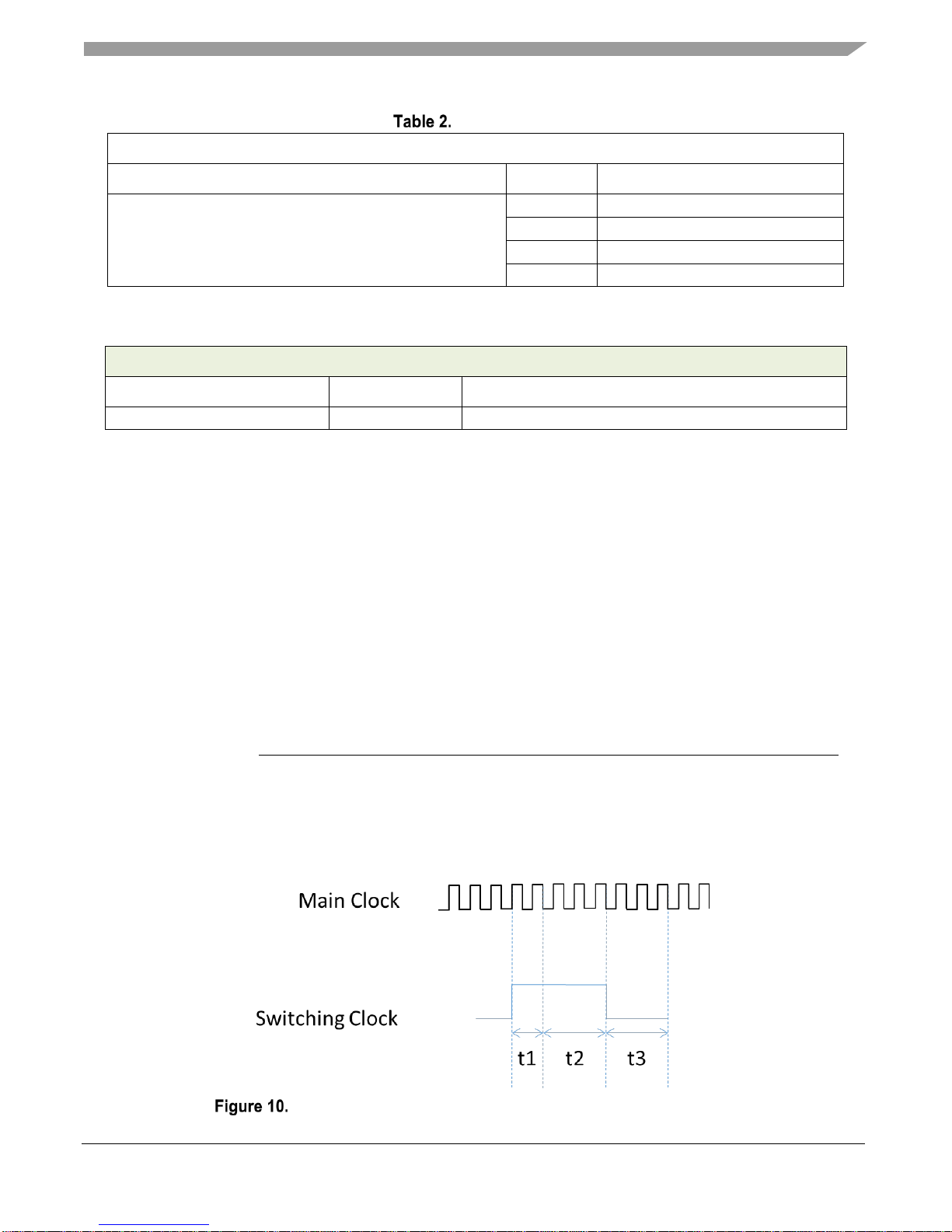
•T3: Configurable, SSC output low period
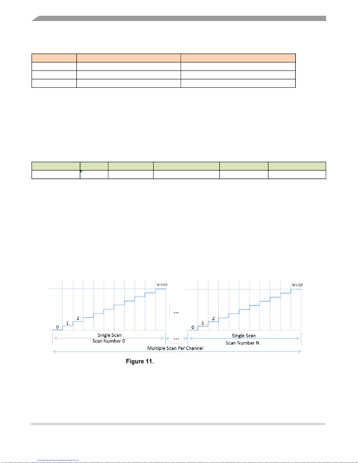
The basic formula of the scan time is listed below, Tnstep is the time costed of TSI single scan:
•Fsw: Configurable, the switching clock frequency.
For example, Ci=90pF, vp-vm=1v, Rs=10k, dV=100mV, M_L/M_R=4, Tsw/T3=4, so it will cost 160us
single scan time for TSI mutual mode.
2.2.2. Sensitivity boost
If the mutual touch sensor intrinsic sensitivity is limited due to parasitic, sensitivity boost feature can be
activated by setting M_SEN_BOOST<4:0>. The basis average charge current will be subtracted by
boost current which enlarge the signal current.
In one typical case, ΔV=100mV, Rs=10k, Vp-Vm=1V, Fsw=1MHz, Ci=90pF,
M_PMIRRORL=16, M_PMIRRORR= M_NMIRROR= 2; Dec=8, Order=2.
NSTEP=72; TSICNT=4608;
Note: Keep M_PMIRRORR and M_NMIRROR the same.
3.TSI software configurations
3.1. Self-capacitive mode configurations
The software configurations for the self-capacitive mode include:
clock generation
scan time
comparator
sensitivity boost
Attached below is an example of the configurations for the self-capacitive mode.