OEC UroView®2800 Table/Generator Functional Block Diagrams
2
Service
Periodic Maintenance
Contents
Schematics
Illustrated Parts
Installation
System CPUs – Collimator Interface PCB .......................................................................................................................................31
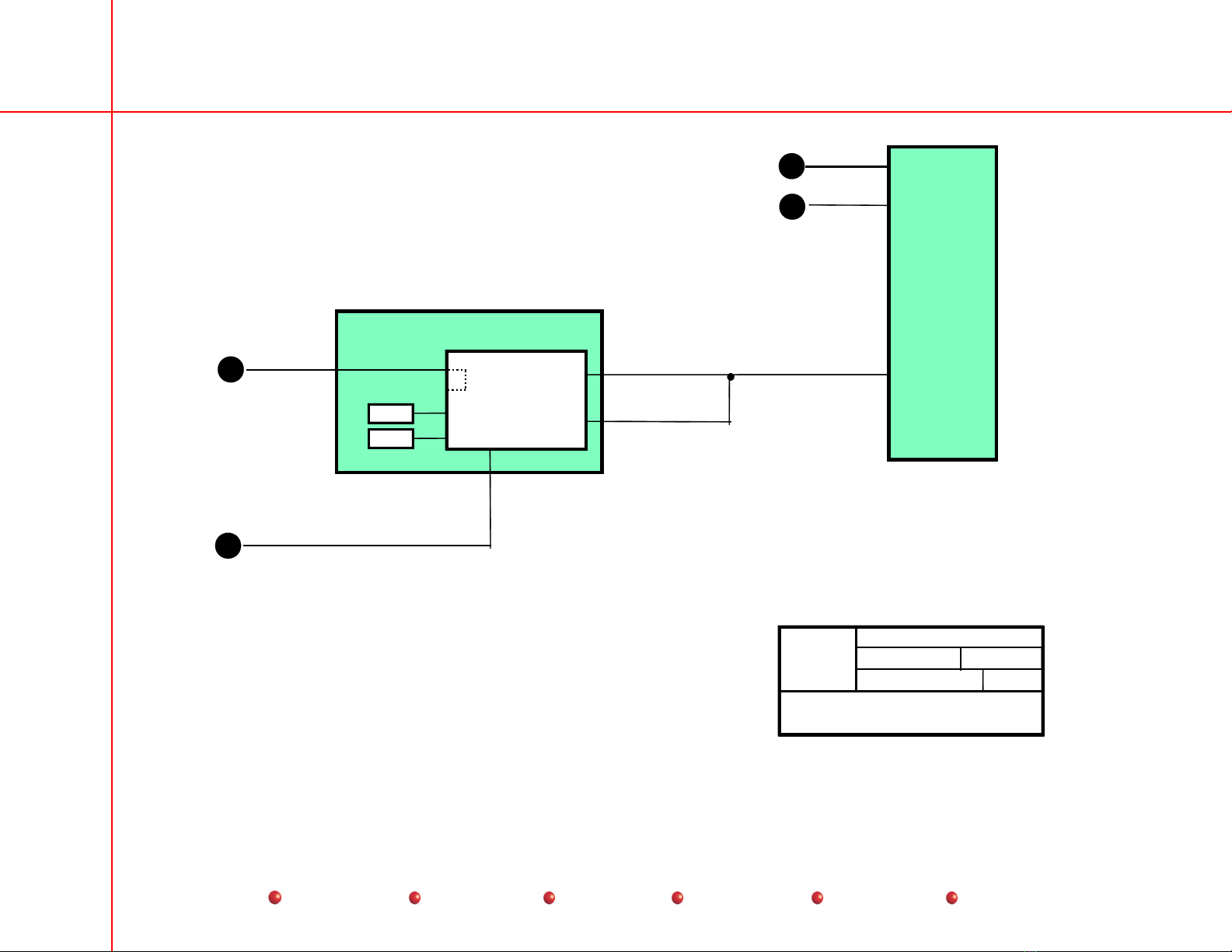
System CPUs – X-ray Control Interface...........................................................................................................................................32
System CPUs – Generator – Generic Interface PCB.......................................................................................................................33
System CPUs – Generator – kV Control PCB .................................................................................................................................34
System Communications – System Interface PCB – ARCNET .......................................................................................................35
System Communications – Table/Generator Interface PCB............................................................................................................36
System Communications – Table/Generator Interface PCB............................................................................................................37
System Communications – X-ray Control Interface PCB.................................................................................................................38
System Communications – Collimator Interface PCB – ARCNET...................................................................................................39
System Communications –ARCNET Signals...................................................................................................................................40
X-ray Tube Stator Control and Temperature Sensing......................................................................................................................41
X-ray On – Table/Generator Interface PCB .....................................................................................................................................42
X-ray On – Generator.......................................................................................................................................................................43
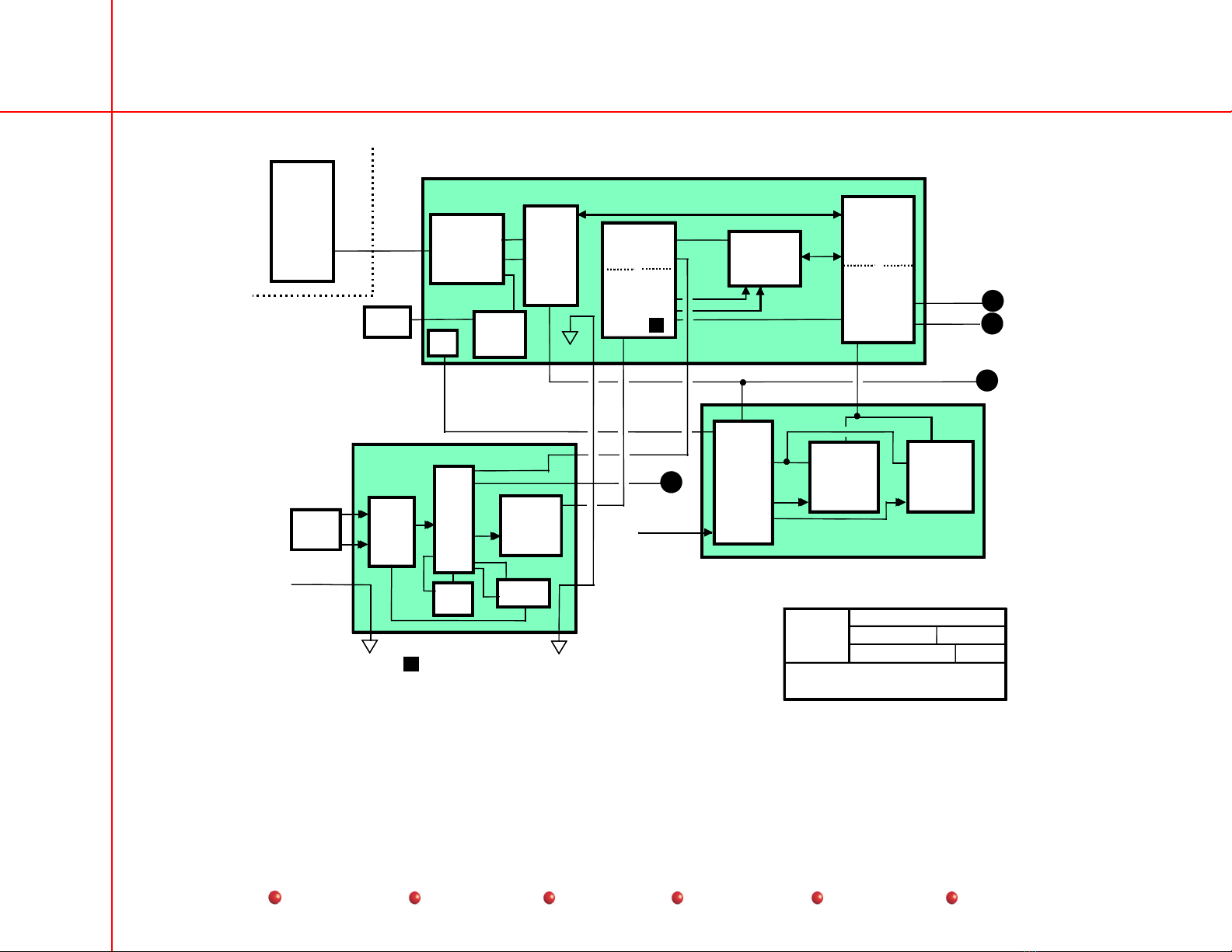
kV Generation Functional Diagram – Table/Generator Interface & Generic Interface PCB ............................................................44
kV Generation Functional Diagram – kV Control Board...................................................................................................................45
kV Generation Functional Diagram – kV Measure PCB & Gate Command PCB ............................................................................46
kV Generation Functional Diagram – AC/DC PCB & Resonant Circuit Power Components...........................................................47
mA Generation Functional Diagram – Table/Generator Interface & Generic Interface PCB ...........................................................48
mA Generation Functional Diagram – kV Control Board & LVPS....................................................................................................49
mA Generation Functional Diagram – kV Measure PCB, Heater boards, & LVPS..........................................................................50
mA Generation Functional Diagram – Heater Board LEDs..............................................................................................................51
mA Generation Functional Diagram – LVPS400 LEDs....................................................................................................................52
mA Generation Functional Diagram – kV Control Board LEDs........................................................................................................53
ABS Path – Video Path....................................................................................................................................................................54
ABS Path..........................................................................................................................................................................................55
Image Intensifier – Mag Mode Control.............................................................................................................................................56
Image Path - Functional Diagram Map ............................................................................................................................................57
Image Path Overview.......................................................................................................................................................................58
Image Path into Video Controller PCB.............................................................................................................................................59
Image Path Out of Video Controller PCB.........................................................................................................................................60
Image Path in Display Adapter PCB ................................................................................................................................................61
Image Path Waveforms....................................................................................................................................................................62
AEC Functional Diagram..................................................................................................................................................................63