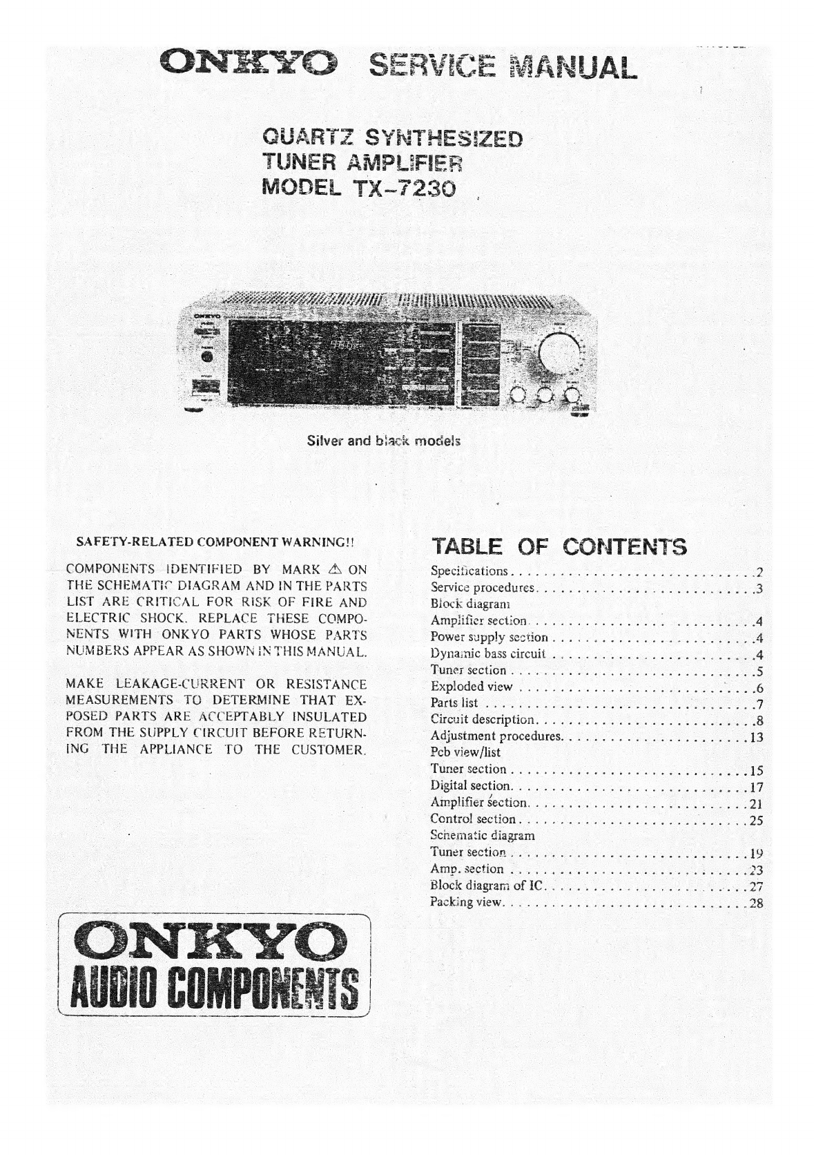
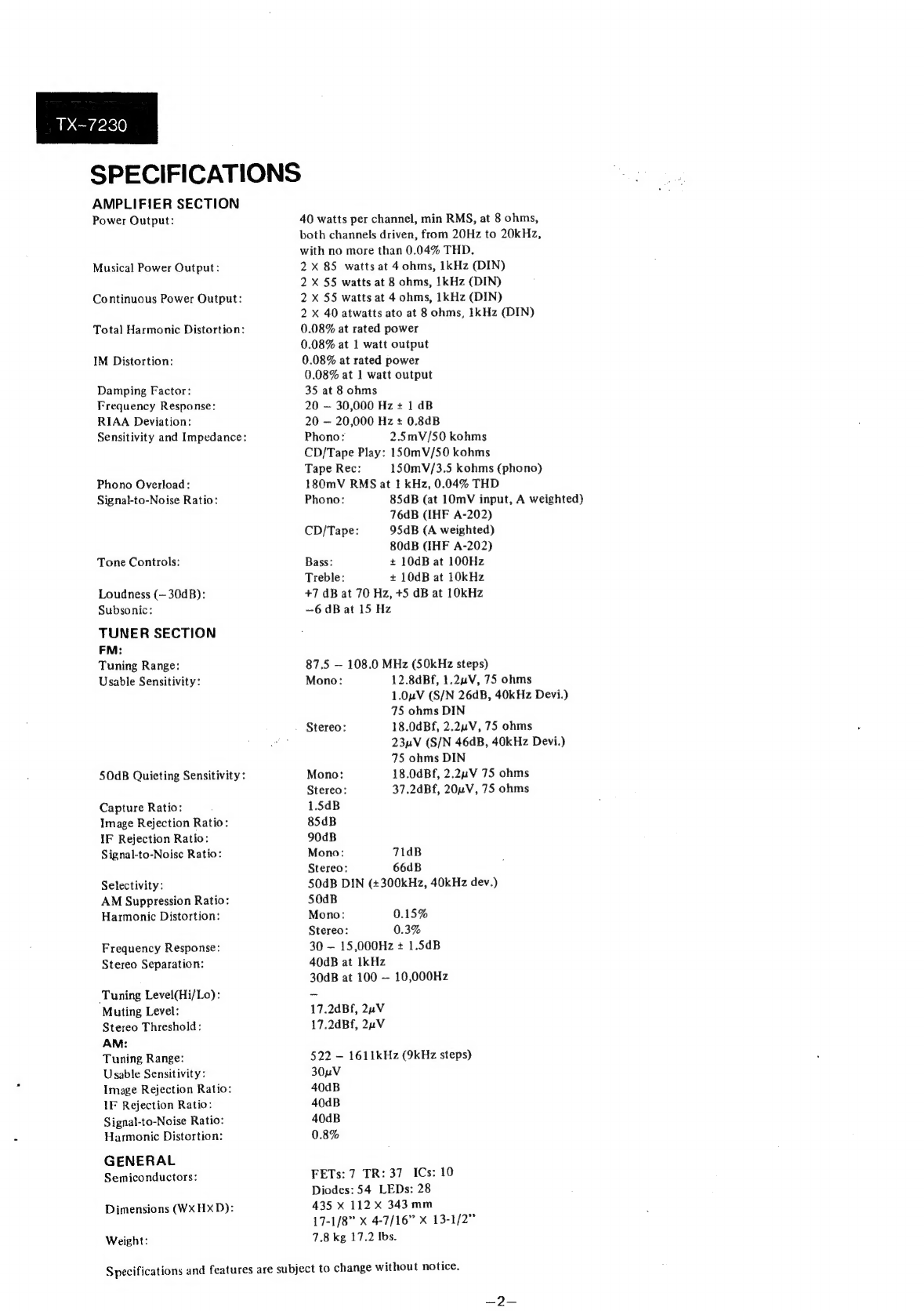
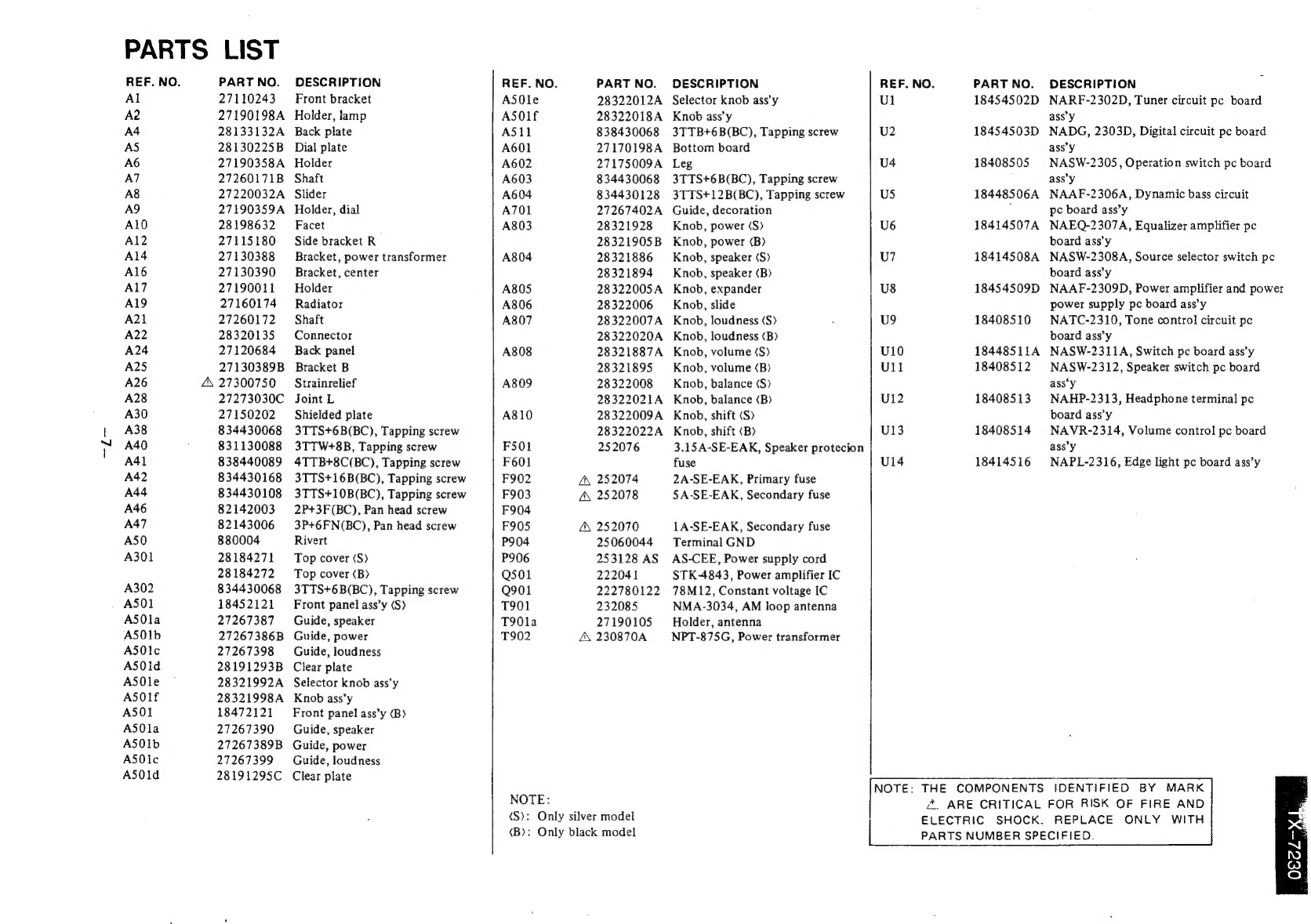
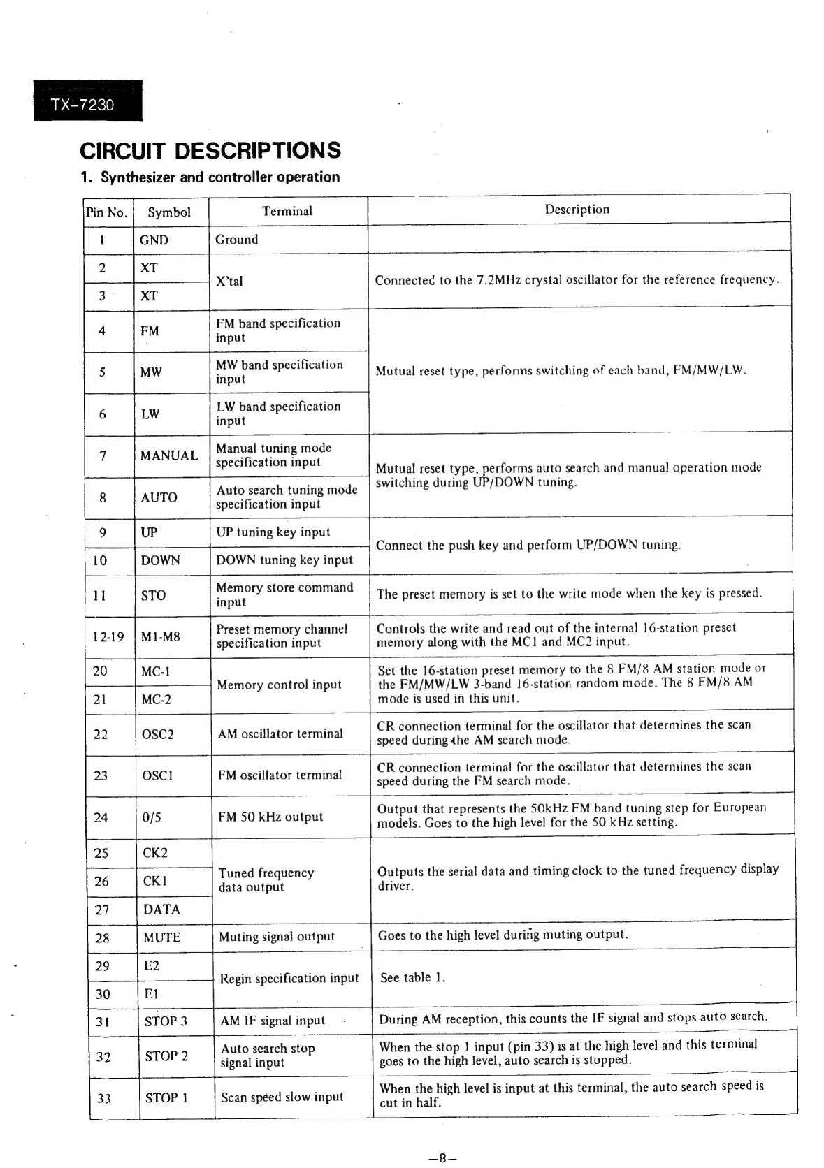
Onkyo TX-7230 User manual
Other Onkyo Amplifier manuals

Onkyo
Onkyo TX-7900 User manual

Onkyo
Onkyo A-8700 User manual

Onkyo
Onkyo A-7 User manual

Onkyo
Onkyo A-5VL - Integrated Stereo Amplifier User manual

Onkyo
Onkyo A-8500 User manual

Onkyo
Onkyo A-9000R User manual

Onkyo
Onkyo TX-906 User manual

Onkyo
Onkyo P-3000R User manual

Onkyo
Onkyo A-9150 User manual

Onkyo
Onkyo A-7090 User manual