6
V 1.03 - eng
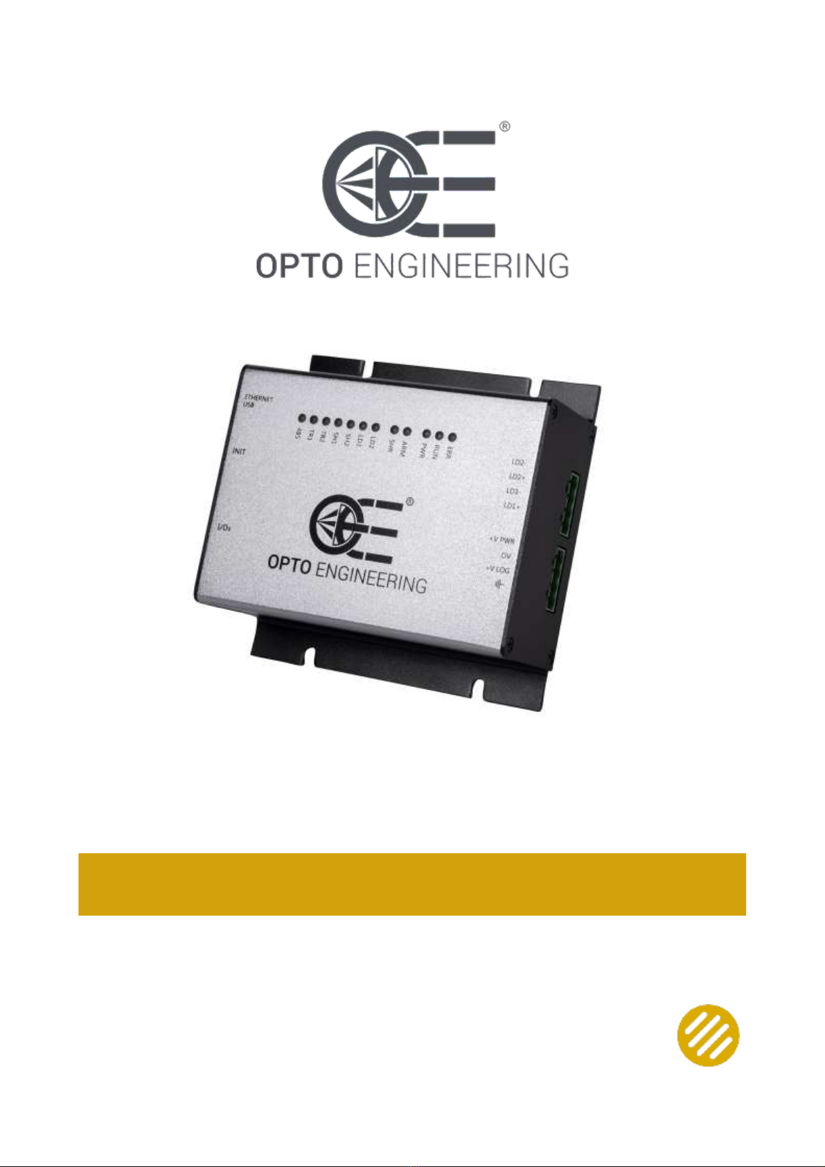
LTDVE2CH-20F | INSTRUCTIONS MANUAL
4. General description
Any machine vision application employs some kind of light controller. Light controllers are widely
used to both optimize illumination intensity and obtain repeatable trigger sequencing between lights
and vision cameras.
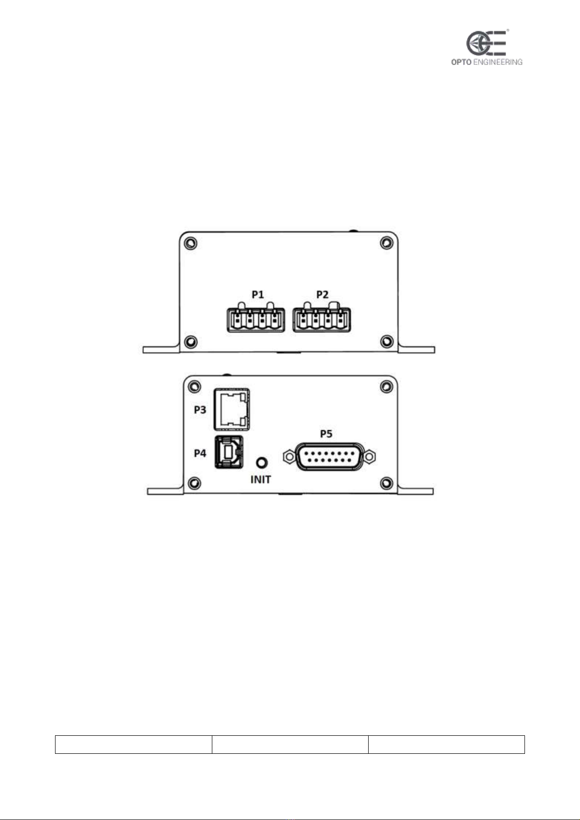
This controller is a compact unit that includes power supply conditioning, intensity control, timing
generation and advanced triggering functions.
The controller can be set up using a PC with serial RS485 or Ethernet interfaces. Configurations are
saved in non-volatile memory so that the controller will resume operation after a power cycle.
4.1. Benefits of current control
Most LED manufacturers suggest their products to be driven using a constant current source, not a
constant voltage source. This is because, using a constant voltage driving, small variations in
temperature or voltage at the LEDs can cause a noticeable change in their brightness.
Brightness control with voltage is also very difficult because of the non-linearity of brightness with
voltage. On the contrary, the brightness is approximately linear with current, so by driving the LEDs
with a known current, intensity control is linear.
4.2. Operating mode
This strobe controller has two programmable, current-controlled light outputs. The two light outputs
can be used in pulsed or continuous mode.
In pulsed mode the light is switched on only when necessary. A digital input is used as a trigger
source. When a rising or falling edge on the trigger signal is detected the output is pulsed for the
programmed amount of time.
Using this technique, it is possible to obtain excellent steady images of moving objects. The camera
can be set for an arbitrary long exposure time and the light turned on for a shorter time, just enough
to freeze the motion. This helps to overcome the uncertainty issues usually related with integration
start which, to some degree, afflict most commercial cameras.
The delay from the trigger to the output pulse, the width of the output pulse and the intensity of the
output pulse are all independently configurable. The pulse delay can range from 0 µs to 1 s. The
pulse width can range from 1 µs to 1 s.
In continuous mode the light is always switched on, independently from the trigger signal. Using this
technique, the maximum current value for each channel has to be limited in order to prevent the
overheating of the controller.
The two output drivers in the controller can either operate in two modes: independent mode and
shared mode. In independent mode, the two light outputs are completely autonomous and currents
and timings are independent.
In the shared mode the two output drivers are interconnected. This results in twice the maximum
output current than in the independent mode. In the shared mode, the controller effectively behaves
as a single channel controller.
In either independent mode or shared mode there are two current ranges. In independent mode the
current ranges are:
Low current, up to 250 mA (with a resolution of 1 mA)
High current, up to 20 A (with a resolution of 20 mA)
In shared mode the current ranges are:
Low current, up to 500 mA (with a resolution of 2 mA)