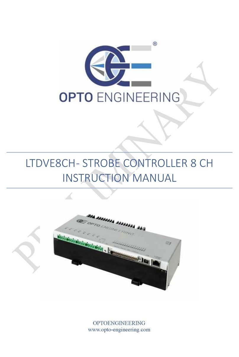
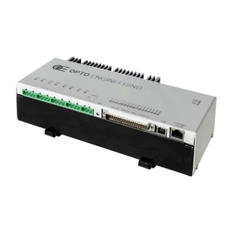
opto engineering LTDVE4CH-20 User manual

ACCESSORIES
INSTRUCTIONS MANUAL
Strobe controller 4 CH
LTDVE4CH-20

1
LTDVE4CH-20 | INSTRUCTIONS MANUAL
INDEX
1. Disclaimer ................................................................................................ 4
2. Safety notes ............................................................................................. 4
3. Product end-of-life handling ................................................................... 4
4. General description ................................................................................. 5
4.1. Benefits of current control ....................................................................................................5
4.2. Operating mode ...................................................................................................................5
5. Getting started ......................................................................................... 5
6. Mechanical fixing..................................................................................... 6
7. Heat dissipation ....................................................................................... 6
7.1. Calculating generated heat per channel ...............................................................................6
7.2. Reducing generated heat .....................................................................................................7
8. Connections............................................................................................. 7
8.1. Layout of connectors............................................................................................................7
8.2. Power and logic supply ........................................................................................................8
8.3. Light outputs ........................................................................................................................9
8.3.1. Light outputs 1 and 2.....................................................................................................9
8.3.2. Light outputs 3 and 4.....................................................................................................9
8.4. Input/output synchronization...............................................................................................10
8.4.1. Synchronization inputs ................................................................................................10
8.4.2. Synchronization outputs .............................................................................................. 11
8.4.3. Serial RS485 interface.................................................................................................12
8.4.4. External temperature sensor .......................................................................................13
8.5. Cable size and length.........................................................................................................13
9. Communication interfaces.................................................................... 14
9.1. Serial RS485 interface .......................................................................................................14
9.2. Ethernet interface...............................................................................................................14
10. Visual indicators .................................................................................. 15
11. INIT button functions ........................................................................... 16
12. Pulse shaping logic ............................................................................. 16
12.1. Diagram of internal logic...................................................................................................16
12.2. Input filters .......................................................................................................................17
12.3. Input multiplexers .............................................................................................................18
12.4. Pulse generator................................................................................................................18
12.5. Output multiplexers ..........................................................................................................19
12.6. Output protection..............................................................................................................19
12.7. Free running oscillator......................................................................................................21

2
LTDVE4CH-20 | INSTRUCTIONS MANUAL
13. Wiring diagrams................................................................................... 21
13.1. Wiring example #1: controller triggers camera..................................................................21
13.2. Wiring example #2: camera triggers controller..................................................................22
14. Operation.............................................................................................. 23
14.1. Operation with Modbus ....................................................................................................23
14.1.1. Comparison of Modbus/RTU, Modbus/TCP and Modbus/UDP ..................................23
14.1.2. Supported function codes..........................................................................................23
14.1.3. Read Holding Registers (0x03)..................................................................................24
14.1.4. Write Single Register (0x06)......................................................................................24
14.1.5. Write Multiple Registers (0x10)..................................................................................24
14.2. Register file ......................................................................................................................24
14.2.1. Register DEVICE_TYPE............................................................................................34
14.2.2. Register BOOT_VERSION ........................................................................................35
14.2.3. Register MCU_VERSION ..........................................................................................35
14.2.4. Register FPGA_VERSION ........................................................................................35
14.2.5. Register BOARD_VERSION .....................................................................................35
14.2.6. Register OSC_PERIOD.............................................................................................35
14.2.7. Registers FILTER_SEL[0:3].......................................................................................35
14.2.8. Registers INPUT_SEL[0:7] ........................................................................................35
14.2.9. Registers GEN_DLY_BASE[0:7]................................................................................36
14.2.10. Registers GEN_DLY_CNT[0:7]................................................................................37
14.2.11. Registers GEN_WDT_BASE[0:7] ............................................................................37
14.2.12. Registers GEN_WDT_CNT[0:7] ..............................................................................38
14.2.13. Registers OUTPUT_SEL_HI[0:3] and OUTPUT_SEL_HI[8:11]................................38
14.2.14. Registers OUTPUT_SEL_LO[0:3] and OUTPUT_SEL_LO[8:11] .............................39
14.2.15. Registers PRT_CNT_ON[0:3]..................................................................................39
14.2.16. Registers PRT_ENA_ON[0:3]..................................................................................40
14.2.17. Registers PRT_CNT_OFF[0:3] ................................................................................40
14.2.18. Registers PRT_ENA_OFF[0:3] ................................................................................40
14.2.19. Registers CUR_RANGE[0:3] ...................................................................................40
14.2.20. Registers CUR_VALUE[0:3] ....................................................................................41
14.2.21. Register RS485_MODBUS_ADDR..........................................................................41
14.2.22. Register RS485_LINE_SPEED ...............................................................................41
14.2.23. Register RS485_LINE_PARITY...............................................................................42
14.2.24. Registers ETH_MAC_ADDR[0:2] ............................................................................42
14.2.25. Registers ETH_HOSTNAME[0:7] ............................................................................42
14.2.26. Register ETH_DHCP_ENABLE ...............................................................................43
14.2.27. Register ETH_IP_ADDR_HI ....................................................................................43
14.2.28. Register ETH_IP_ADDR_LO ...................................................................................43

3
LTDVE4CH-20 | INSTRUCTIONS MANUAL
14.2.29. Register ETH_SUBNET_MASK_HI .........................................................................43
14.2.30. Register ETH_SUBNET_MASK_LO ........................................................................43
14.2.31. Register ETH_DEF_GATEWAY_HI .........................................................................43
14.2.32. Register ETH_DEF_GATEWAY_LO ........................................................................43
14.2.33. Register ETH_PRI_DNS_HI ....................................................................................43
14.2.34. Register ETH_PRI_DNS_LO...................................................................................44
14.2.35. Register ETH_SEC_DNS_HI...................................................................................44
14.2.36. Register ETH_SEC_DNS_LO..................................................................................44
14.2.37. Register ETH_MODBUS_ADDR .............................................................................44
14.2.38. Register ETH_MODBUS_TCP_PORT.....................................................................44
14.2.39. Register ETH_MODBUS_UDP_PORT ....................................................................44
14.2.40. Registers WEB_PASSWORD[0:3] ...........................................................................44
14.2.41. Register REMOTE_TEMPERATURE ......................................................................45
14.2.42. Register BOARD_TEMPERATURE[0:1] ..................................................................45
14.2.43. Register SUPPLY_VOLTAGE ..................................................................................45
14.2.44. Registers MEASURED_CURRENT[0:3] ..................................................................45
14.2.45. Registers MEASURED_VOLTAGE[0:3] ...................................................................46
14.2.46. Register ERROR_WORD ........................................................................................46
14.2.47. Registers CALIB_CUR_ADD[0:3] ............................................................................47
14.2.48. Registers CALIB_CUR_MUL[0:3] ............................................................................47
14.2.49. Registers CALIB_VLT_ADD[0:3] .............................................................................47
14.2.50. Registers CALIB_VLT_MUL[0:3] .............................................................................47
14.2.51. Register CALIB_UNLOCK .......................................................................................47
14.2.52. Register BOARD_COMMAND.................................................................................47
14.3. Operation with a web browser ..........................................................................................48
14.3.1. Main page and navigation menu................................................................................48
14.3.2. Setup synch inputs TR1-TR4.....................................................................................50
14.3.3. Setup pulse generators GN1-GN4.............................................................................51
14.3.4. Setup pulse generators GN5-GN8.............................................................................53
14.3.5. Setup light outputs LD1-LD4......................................................................................53
14.3.6. Setup synch outputs SH1-SH4 ..................................................................................55
14.3.7. General setup............................................................................................................56
14.3.8. Advanced setup.........................................................................................................58
15. Electromagnetic compatibility ............................................................ 60
16. Firmware update procedure................................................................ 60

4
LTDVE4CH-20 | INSTRUCTIONS MANUAL
1. Disclaimer
Always deploy and store Opto Engineering products in the prescribed conditions in order to ensure
proper functioning. Failing to comply with the following conditions may shorten the product lifetime
and/or result in malfunctioning, performance degradation or failure.
Ensure that incorrect functioning of this equipment cannot cause any dangerous situation or
significant financial loss to occur. It is essential that the user ensures that the operation of the
controller is suitable for their application. All trademarks mentioned herein belong to their respective
owners.
Except as prohibited by law:
•All hardware, software and documentation are provided on an “as is” basis
•Opto Engineering accepts no liability for consequential loss, of any kind
Upon receiving your Opto Engineering product, visually examine the product for any damage during
shipping. If the product is damaged upon receipt, please notify Opto Engineering immediately.
2. Safety notes
Please read the following notes before using this controller. Contact your distributor or dealer for any
doubts or further advice.
This device must not be used in an application where its failure could cause a hazard to human
health or damage to other equipment. Keep in mind that if the device is used in a manner not
foreseen by the manufacturer, the protection provided by its circuits and by its enclosure may be
impaired.
This is a low voltage device. As such, the potential difference between any combination of applied
signals must not exceed, at all times, the supply voltage. Higher voltages may cause a fault and can
be dangerous to human health.
This device has limited protection against transients caused by inductive loads. If necessary, use
external protection devices like fast diodes or, better, specific transient protectors.
The controller outputs pulses with high energy content. The user must be careful to connect the
inputs and outputs correctly and to protect the output wiring and load from unintentional short-
circuits. When the device is switched off, there is still energy stored in the internal capacitors for at
least five minutes.
When operating the controller at the maximum ratings it can get very hot. The controller should be
positioned where personnel cannot accidentally touch it and away from flammable materials. Never
exceed the power ratings stated in the manual.
3. Product end-of-life handling
Observe the following guidelines when recycling this equipment or its components.
Production of this equipment required the extraction and use of natural resources. The equipment
may contain substances that could be harmful to the environment or human health if improperly
handled at the product’s end of life. In order to avoid release of such substances into the environment
and to reduce the use of natural resources, we encourage you to recycle this product in an
appropriate system that will ensure that most of the materials are reused or recycled appropriately.
This symbol indicates that this product complies with the applicable European Union
requirements according to the WEEE (Waste Electrical and Electronic Equipment)
Directive 2012/19/EU

5
LTDVE4CH-20 | INSTRUCTIONS MANUAL
4. General description
Any machine vision application employs some kind of light controller. Light controllers are widely
used to both optimize illumination intensity and obtain repeatable trigger sequencing between lights
and vision cameras.
This controller is a compact unit that includes power supply conditioning, intensity control, timing
generation and advanced triggering functions.
The controller can be set up using a PC with serial RS485 or Ethernet interfaces. Configurations are
saved in non-volatile memory so that the controller will resume operation after a power cycle.
4.1. Benefits of current control
Most LED manufacturers suggest their products to be driven using a constant current source, not a
constant voltage source. This is because, using a constant voltage driving, small variations in
temperature or voltage at the LEDs can cause a noticeable change in their brightness.
Brightness control with voltage is also very difficult because of the non-linearity of brightness with
voltage. On the contrary, the brightness is approximately linear with current, so by driving the LEDs
with a known current, intensity control is linear.
This strobe controller has four independent, programmable, current-controlled pulsed or continuous
outputs with currents ranging from zero up to 20 A. In continuous mode the output current is internally
limited by the firmware to 2 A.
4.2. Operating mode
This controller operates both in pulsed and in continuous mode.
In pulsed mode the light is switched on only when necessary. A digital input is used as a trigger.
When a rising edge on the trigger signal is detected the output is pulsed for the programmed amount
of time.
Using this technique, it is possible to obtain excellent steady images of moving objects. The camera
can be set for an arbitrary long exposure time and the light turned on for a shorter time, just enough
to freeze the motion. This helps to overcome the problems usually related with integration start
uncertainty which, to some degree, afflict most commercial cameras.
The delay from the trigger to the output pulse, the width of the output pulse and the intensity of the
output pulse are all independently configurable. The pulse delay can range from 0 µs to 1 s. The
pulse width can range from 1 µs to 1 s. There are three ranges for the current pulse:
Low current, up to 200 mA (with resolution of 1 mA)
Mid current, up to 4 A (with resolution of 4 mA)
High current, up to 20 A (with resolution of 20 mA)
In continuous mode the light is always switched on, independently from the trigger signal. Using this
technique, the maximum current value for each channel has to be limited in order to prevent the
overheating of the controller. For more information about current and power limitations refer to
chapter 7.
5. Getting started
Carefully read the sections on Safety Notes and Heat Dissipation and check the product fits your
needs. Mount the controller using a DIN rail as described in the section on Mechanical fixing.
Connect the controller as in the section on Connections. When the controller powers up it should
show the PWR LED lit with a stable green colour and the RUN LED lit with a pulsing green colour.
Read the section on Operation. The controller can be configured by using both a serial RS485
6
LTDVE4CH-20 | INSTRUCTIONS MANUAL
interface and an Ethernet interface (see chapter 9).
6. Mechanical fixing
The controller must be mounted on a DIN rail. Allow free flow of air around the unit. The controller
has an IP rating of 20 and should be installed so that moisture and dirt cannot enter it.
An enclosure may also be required for other parts of the system such as power supplies. That
enclosure would provide both mechanical and environmental protection in industrial applications.
7. Heat dissipation
The controller integrates several linear circuits to produce the constant current outputs. This means
that it generates heat which needs to be dissipated. The operating temperature range is 0 °C to
40 °C.
The controller can approximately dissipate the following average powers:
30 W at 25 °C (about 7.5 W per channel)
25 W at 40 °C (about 6.3 W per channel)
A simple way to estimate the maximum average power the controller can dissipate is by applying the
following formula:
DissipablePower [W] = (TempHeatsink [°C] – TempAmbient [°C]) / ThResistance [°C/W]
Where:
DissipablePower is the maximum average power the controller can dissipate
TempHeatsink is the maximum temperature of the controller heatsink
TempAmbient is the actual temperature of the ambient where the controller is placed
ThResistence is the thermal resistance between the heatsink and the ambient
For the LTDVE series the ThResistance parameter is about 1.91 °C/W.
The maximum permissible controller heatsink temperature is 90 °C. If the heatsink temperature rises
above 90 °C, the controller switches off all the output channels. Output channels are then reactivated
once temperature falls below 80 °C.
If the average power that must be dissipated is greater than the previously stated value, a different
and more efficient cooling system is required. Solutions could be the use of a cooling fan (active
cooling system) or the use of a bigger heatsink (passive cooling system).
The controller can be powered with supply voltages between 24 V and 48 V. This allows a large
number of different lights to be efficiently driven. Take care of the actual supply voltage when
calculating the generated heat.
7.1. Calculating generated heat per channel
For a pulsed output, the average power that is transformed to heat and then must be dissipated can
be calculated using the following formula:
Heat [W] = LightCurrent [A] * (SupplyVoltage [V] – LightVoltage [V]) * DutyCycle [·]
Where:
LightCurrent is the illuminator operating current
LightVoltage is the illuminator operating voltage
SupplyVoltage is the actual supply voltage (from 24 V to 48 V)

7
LTDVE4CH-20 | INSTRUCTIONS MANUAL
DutyCycle is the actual duty cycle
The duty cycle is given by:
DutyCycle [·] = PulseWidth [s] * TriggerFrequency [Hz]
If the output is driven in continuous mode, the previous equations are still valid but the parameter
DutyCycle becomes one because the output is always active.
The parameters LightCurrent and LightVoltage are light specific and should be either given in the
light documentation or measured experimentally.
7.2. Reducing generated heat
The total heat generated by the controller is simply given by adding the generated heat for each of
the four channels, as calculated in the previous section.
There are several ways to reduce the heat generated by the controller. The simplest way would be
to turn the light off when not needed. If the light is on only when necessary the generated heat can
be drastically diminished. Another opportunity would be to reduce pulse width or output current, if
permitted by the application.
Another strategy to reduce the generated heat would be to connect lights in series instead of parallel,
if possible. If you have several lights connected in parallel then changing the arrangement to series
will increase the voltage across them but also reduce the overall current.
The last option, feasible with this four channels controller, would be to use two or more controllers
and use just a few channels from each. For high power applications this may be the only solution.
8. Connections
See the next sections for information about connections. All connections are made via screw
terminals on the front panel of the controller. Check all connections carefully before switching on the
equipment.
The controller has two 24 V to 48 V supplies for the power and logic sections. This is to increase
versatility. Supply to the logic section should always be present, while supply to the power stages
can be cut off at any time. Supply to the power stages can be removed to protect the end user from
photo-biological hazard and other dangerous situations that may happen during fault conditions.
These two supplies can be connected together if convenient. For convenience, they share a common
negative terminal.
8.1. Layout of connectors
The drawing in Figure 1: connectors on the controller front panel depicts all the controller
connections, which are easily accessible on the front panel. As indicated in the drawing, connectors
are identified by their unique designators (P1, P2, P3, P4, P5 and P6).

8
LTDVE4CH-20 | INSTRUCTIONS MANUAL
Figure 1: connectors on the controller front panel
The connectors are briefly described below. A detailed description follows in the next sections.
Connectors P1 and P2 are used to connect the four illuminators
Connector P3 is used to supply power
Connector P4 is used for input/output synchronization and for serial RS485 communication
Connector P5 is a USB port (B type), not active at the moment
Connector P6 is an Ethernet RJ45 jack
For connectors P1, P2, P3 and P4 a mating plug is provided in the controller package. For
convenience the relevant manufacturer part numbers are listed in Table 1: mating plugs for the
controller connectors. Even if equivalent mating plugs may be available, these are the recommended
components.
Connector designator
Manufacturer
Mating plug part number
P1, P2
Phoenix Contact
1757035
P3
Phoenix Contact
1757022
P4
MH Connectors
MHDM25SS
Table 1: mating plugs for the controller connectors
8.2. Power and logic supply
The power supply voltage must be between 24 V and 48 V. A dedicated and well-regulated switching
power supply is required. The external power supply must be capable of supplying the average and
peak currents needed for all active light outputs.
Choose a power supply unit that limits its output current by design or use protecting fuses. The fuses
should be appropriately de-rated if mounted in an enclosure, as the inside temperature can be higher
than the ambient temperature.
Ensure that the wire gauge used for these power connections is appropriate for the current to be

9
LTDVE4CH-20 | INSTRUCTIONS MANUAL
drawn. The power supply low voltage and mains wiring should be separately routed.
Power supply is delivered to the controller using the screw terminals of connector P3. Connector
pinout, ordered from left to right, is listed in Table 2: pinout of connector P3.
Number
Name
Description
Note
1
+V LOG
Power supply. Positive terminal
Used for logic section
2
0V
Power supply. Negative terminal
3
+V PWR
Power supply. Positive terminal
Used for power stages
Table 2: pinout of connector P3
The controller has two 24 V to 48 V power terminals to independently supply the logic and power
sections. They are named +V LOG and +V PWR. These two supplies can be connected together if
convenient. They share the common negative terminal named 0V. It must be connected to the power
supply negative.
Ensure that the polarity of +V LOG, +V PWR and 0V is correct.
8.3. Light outputs
Light outputs are paired on the two 4-way pluggable screw terminal sockets named P1and P2. It is
possible to use two 2-way connectors in a 4-way socket. The light output connections must not be
paralleled or grounded in any way.
The state of each output is shown by a yellow LED indicator next to the connector.
Make sure you set the correct current rating for a light before using it. See the light datasheet and
manual for details on this topic.
8.3.1. Light outputs 1 and 2
Light outputs 1 and 2 are available on the LD1+, LD1-, LD2+ and LD2- screw terminals of connector
P1. Connector pinout, ordered from left to right, is listed in Table 3: pinout of connector P1. Be careful
not to cross-connect the two lights.
Number
Name
Description
Note
1
LD1+
Power channel 1 output. LED anode
2
LD1-
Power channel 1 output. LED cathode
3
LD2+
Power channel 2 output. LED anode
4
LD2-
Power channel 2 output. LED cathode
Table 3: pinout of connector P1
Please note that LED1- and LED2- are not the same as 0V.
8.3.2. Light outputs 3 and 4
Light outputs 3 and 4 are available on the LD3+, LD3-, LD4+ and LD4- screw terminals of connector
P2. Connector pinout, ordered from left to right, is listed in Table 4: pinout of connector P2. Be careful
not to cross-connect the two lights.

10
LTDVE4CH-20 | INSTRUCTIONS MANUAL
Number
Name
Description
Note
1
LD3+
Power channel 3 output. LED anode
2
LD3-
Power channel 3 output. LED cathode
3
LD4+
Power channel 4 output. LED anode
4
LD4-
Power channel 4 output. LED cathode
Table 4: pinout of connector P2
Please note that LED3- and LED4- are not the same as 0V.
8.4. Input/output synchronization
Connector P4 is used for input and output synchronization and for serial RS485 communication.
There are four independent, galvanically isolated, synchronization inputs. These inputs can be
connected directly to the system for voltages up to 24V. An external series resistor is not necessary.
Synchronization inputs may be left unconnected when not used. The state of each synchronization
input is shown by a green LED indicator next to the connector.
There are four independent, galvanically isolated, synchronization outputs. These outputs can be
used, for example, to trigger a camera or a slave controller. These outputs can be connected directly
to the system for voltages up to 60V. The state of each synchronization output is shown by a yellow
LED indicator next to the connector.
Connector P4 also provides three signals for an isolated serial RS485 interface and two signals for
an optional and non-electrically isolated external temperature sensor. The activity of the serial RS485
interface is shown by a dedicated yellow LED next to connector P4.
See the following section for more information about connector P4.
8.4.1. Synchronization inputs
The four synchronization inputs are available on the TR1+, TR1-, TR2+, TR2-, TR3+, TR3-, TR4+
and TR4- terminals of connector P4. These signals are listed in Table 5: pinout of connector P4 for
synchronization inputs. Be careful not to cross-connect the four synchronization inputs.
Pin number
Name
Description
1
TR1-
Input 1. Negative terminal
14
TR1+
Input 1. Positive terminal
2
TR2-
Input 2. Negative terminal
15
TR2+
Input 2. Positive terminal
3
TR3-
Input 3. Negative terminal
16
TR3+
Input 3. Positive terminal
4
TR4-
Input 4. Negative terminal
17
TR4+
Input 4. Positive terminal
Table 5: pinout of connector P4 for synchronization inputs

11
LTDVE4CH-20 | INSTRUCTIONS MANUAL
The schematic of Figure 2: interface circuits for input synchronization depicts the internal input
circuits. An internal constant current generator connected in series with each input allows for a broad
range of input voltages without any need for a series resistor. These inputs can be directly driven by
voltages up to 24V.
Figure 2: interface circuits for input synchronization
Circuit specifications are summarized in Table 6: specifications of input synchronization circuits.
Please note the reported values are typical.
Parameter
Value
Unit
Note
Uin (low)
0–1
V
-
Uin (high)
3.3–24
V
-
Iin
5–9
mA
Internal constant-current generator
Table 6: specifications of input synchronization circuits
8.4.2. Synchronization outputs
The four synchronization outputs are available on the SH1+, SH1-, SH2+, SH2-, SH3+, SH3-, SH4+
and SH4- terminals of connector P4. These signals are listed in the Table 7: pinout of connector P4
for synchronization outputs. Be careful not to cross-connect the four synchronization outputs.
Pin number
Name
Description
5
SH1-
Output 1. Emitter terminal
18
SH1+
Output 1. Collector terminal
6
SH2-
Output 2. Emitter terminal
19
SH2+
Output 2. Collector terminal

12
LTDVE4CH-20 | INSTRUCTIONS MANUAL
7
SH3-
Output 3. Emitter terminal
20
SH3+
Output 3. Collector terminal
8
SH4-
Output 4. Emitter terminal
21
SH4+
Output 4. Collector terminal
Table 7: pinout of connector P4 for synchronization outputs
The schematic of Figure 3: interface circuits for output synchronization depicts the internal output
circuits. These outputs can be directly connected to voltages up to 60V.
Figure 3: interface circuits for output synchronization
Circuit specifications are summarized in Table 8: specifications of output synchronization circuits.
Please note the reported values are typical.
Parameter
Value
Unit
Note
Iout (typ)
10
mA
-
Iout (max)
15
mA
-
Uout (max)
30
V
-
Table 8: specifications of output synchronization circuits
8.4.3. Serial RS485 interface
The serial interface is available on the D+, D- and GND terminals of connector P4. These signals
are listed in Table 9: pinout of serial interface in connector P4. Be careful not to cross-connect the
serial interface signals.

13
LTDVE4CH-20 | INSTRUCTIONS MANUAL
Pin number
Name
Description
Note
12
D-
RS485 data signal. Negative terminal
-
13
GND
RS485 reference ground
-
25
D+
RS485 data signal. Positive terminal
-
Table 9: pinout of serial interface in connector P4
The interface is electrically isolated. Note that GND is not the same as 0V.
8.4.4. External temperature sensor
The controller allows for the connection of an external temperature sensor. The intended
temperature sensor is a NTC (Negative Temperature Coefficient) thermistor with coefficients R25 =
10 kΩ and B25/85 = 3610 K. A suitable component is the Vishay NTCS0603E3103FMT.
The signals are listed in Table 10: pinout of external temperature sensor in connector P4. The two
terminals can be connected freely to the external thermistor, as the component is not polarized.
Pin number
Name
Description
11
NTC1
Temperature sensor terminal 1
24
NTC2
Temperature sensor terminal 2
Table 10: pinout of external temperature sensor in connector P4
These two analogue signals are not electrically isolated from the controller electronics. Be careful
not to connect them to any other signal. A malfunction or short circuit may occur.
8.5. Cable size and length
The actual connecting cables must be chosen on the basis of their load sinking current, the length,
the working voltage and the cable materials characteristics. Special ambient conditions may further
restrict the choice to a specific kind of cable.
The Table 11: cable wire size and length lists the recommended wire sizes and maximum allowed
lengths for all the cables coming to and leaving from the controller. American Wire Gauge (AWG) is
the wire measurement system used by the United States and Canada, while mm is the metric system
of measurement used across Europe and in most of the world.
Port
Recommended wire size
Maximum length [m]
mm2
AWG
Power and logic supply
1.5
15
5
Light output
0.75
18
5
Synchronization inputs
0.25
24
5
Synchronization outputs
0.25
24
5
Serial RS485 interface
0.25
24
5
External temperature sensor
0.25
24
5
Table 11: cable wire size and length

14
LTDVE4CH-20 | INSTRUCTIONS MANUAL
For improved immunity against external disturbance sources, use a single shielded cable or multiple
shielded cables, grounded at the end opposite to the controller, on the synchronization inputs,
synchronization outputs, serial RS485 interface and external temperature sensor signals.
9. Communication interfaces
There are several ways to configure the controller.
A first option is to use the serial RS485 interface. To support this interface the controller implements
a subset of the Modbus/RTU (Remote Terminal Unit) slave protocol.
A second option is to use the Ethernet interface. Supported Ethernet speeds are 10 Mbit/s and 100
Mbit/s with auto negotiation. The Ethernet interface allows to configure the controller using the
Modbus/TCP (Transmission Control Protocol) slave protocol, the Modbus/UDP (User Datagram
Protocol) slave protocol or the HTTP (Hyper Text Transfer Protocol) protocol. For supporting the
latter, the controller provides an internal web server accessible by most common web browsers.
The Modbus/RTU, Modbus/TCP and Modbus/UDP protocols are implemented by most
programmable logic controllers (PLCs) with a suitable interface.
The availability of two physical interfaces and four logical protocols makes it easy to integrate the
controller in most vision applications.
See chapter 14 for details on operation with both Modbus and web browser.
9.1. Serial RS485 interface
For the serial RS485 interface, the controller implements a subset of the Modbus/RTU slave protocol
and operates, by default, at 9600 bits per second with even parity. The factory set Modbus address
is 32 and it is saved in the controller non-volatile memory.
The Modbus address is one of the controller parameters and can be changed using any of the
available interfaces. The factory set Modbus address can be restored using the INIT button (see
chapter 11 for a description of the INIT button functionalities).
Please note valid Modbus addresses for slave devices are in the range 1 to 247; remaining
addresses are reserved by the standard for special purposes and must not be used. It is of great
importance to ensure, at the time of assigning the slave address, that there are not two devices with
the same address. In such a case, an abnormal behaviour of the whole serial bus can occur, the
master being then in the impossibility to communicate with all the slaves present on the bus.
The activity of the serial RS485 interface is shown by a dedicated yellow LED next to connector P4.
9.2. Ethernet interface
The Ethernet interface allows to configure the controller using the Modbus/TCP slave protocol, the
Modbus/UDP slave protocol or the HTTP protocol. For the last option, the controller provides an
internal web server accessible by most common web browsers.
To use the interface, connect the controller using a standard Ethernet cable. The default parameters
for the communication are listed in Table 12: default parameters for Ethernet communication.
Parameter
Default Value
Host name
LTDVE4CH-20
DHCP
Disabled
IP address
192.168.0.32
Subnet mask
255.255.255.0
Default gateway
192.168.0.1

15
LTDVE4CH-20 | INSTRUCTIONS MANUAL
Preferred DNS server
192.168.0.2
Alternate DNS server
192.168.0.2
Modbus address
32
Modbus/TCP port
502
Modbus/UDP port
502
Table 12: default parameters for Ethernet communication
The IP address, subnet mask and DHCP use flag are some of the controller parameters and can be
changed using any of the available interfaces. The factory configuration uses the static IP address
192.168.0.32. The factory settings can be restored using the INIT button (see chapter 11 for a
description of the INIT button functionalities).
10. Visual indicators
There are sixteen LEDs on the top panel of the controller and two LEDs embedded in the Ethernet
RJ45 jack. Some of them are used to show that power supplies are available, others are pulsed
when inputs and output are activated, while others are used to indicate activity on the communication
interfaces or fault conditions.
The exact meaning of each of the LEDs is listed in Table 13: meaning of the LEDs. The LEDs of the
top panel of the controller are identified by a unique label printed next to them. The Ethernet ACT
and LINK LEDs are identified by their position relative to the Ethernet RJ45 jack. The ACT LED is at
the left of the jack, while the LINK LED is at the right.
Number
Name
Colour
Description
1
PWR
Green
Stable when logic supply is present
2
RUN
Green
Blinks periodically during normal operation
3
ERR
Red
Stable when power supply missing, blinks in error conditions
4
LD1
Yellow
Pulses when light output 1 is activated
5
LD2
Yellow
Pulses when light output 2 is activated
6
LD3
Yellow
Pulses when light output 3 is activated
7
LD4
Yellow
Pulses when light output 4 is activated
8
TR1
Green
Pulses when synchronization input 1 is activated
9
TR2
Green
Pulses when synchronization input 2 is activated
10
TR3
Green
Pulses when synchronization input 3 is activated
11
TR4
Green
Pulses when synchronization input 4 is activated
12
SH1
Yellow
Pulses when synchronization output 1 is activated
13
SH2
Yellow
Pulses when synchronization output 2 is activated
14
SH3
Yellow
Pulses when synchronization output 3 is activated
15
SH4
Yellow
Pulses when synchronization output 4 is activated
16
485
Yellow
Blinks when there is activity on the serial interface
17
ACT
Yellow
Blinks during Ethernet data transmission
18
LINK
Green
Stable when Ethernet connection established
Table 13: meaning of the LEDs

16
LTDVE4CH-20 | INSTRUCTIONS MANUAL
Either the RUN LED or the ERR LED blinks for 500 ms at power on to identify the source used for
the settings.
The green RUN LED blinks when the controller starts by using the settings stored in the non-volatile
memory (the last configuration saved by the customer). The red ERR LED blinks when the controller
reverts to using the factory settings due to user activation of the INIT button (see next section for
more information on the INIT button) or a corruption in the stored customer settings.
Please note the logic supply must be present in order for all the LEDs to turn on.
11. INIT button functions
The INIT button is used either to restore the factory settings or to activate the firmware update
procedure. The INIT button is sampled once at power up.
If the button is sampled as pressed, the user is given a ten seconds interval to start the firmware
update procedure (see chapter 16). If the firmware update procedure is not started in then ten
seconds interval, the settings are restored to the factory values and the controller resumes normal
operation.
During the ten seconds interval the RUN and ERR LEDs blink at a high rate to emphasize the
circumstance. In the meantime, the use of the serial RS485 interface is restricted to the firmware
update and the Modbus/TCP, Modbus/UDP and HTTP protocols are not available.
The INIT button is concealed by a hole located between the terminal blocks and the shell connector.
12. Pulse shaping logic
Each of the four channels can be individually configured to output pulses based either on a discrete
external trigger signal or an internally-generated trigger. A wide variety of internal triggers can be
produced by configuring the internal pulse shaping logic.
This logic includes eight pulse generators and several multiplexers. The pulse generators allow pulse
delay and width control down to 1 µs resolution. The multiplexers, organized as two routing matrices,
allow for the flexible selection of the pulse generators inputs and outputs.
An output protection circuit, used to prevent the light from getting overheated and thus damaged, is
also included in this logic.
12.1. Diagram of internal logic
The drawing of Figure 4: diagram of internal logic network depicts the logic network built in the
controller.

17
LTDVE4CH-20 | INSTRUCTIONS MANUAL
Figure 4: diagram of internal logic network
The four synchronization inputs are shown at the left (TR1, TR2, TR3 and TR4), while the four light
outputs (LD1, LD2, LD3 and LD4) and the four synchronization outputs (SH1, SH2, SH3 and SH4)
are drawn at the right.
A description of each of the blocks is given in the next sections.
12.2. Input filters
The input filters are used to debounce and remove glitches from the incoming synchronization inputs.
Each of the four synchronization inputs has a dedicated, independent filter.
The algorithm implemented in each of the filters processes the relevant synchronization input with a
finite state machine. A change in the filter output is performed only when the input signal has
remained constant for a defined period of time, called filter time constant. Any pulses shorter than
the filter time constant are thus removed and not passed through.
The diagram in Figure 5: operation of the input filter shows the filter operation on a random input
signal.
Figure 5: operation of the input filter
As visible, the input signal is filtered by looking for pulses that hold the same state for a time of at
least Tfilter before the change in state is passed to the output. Please note there is a fixed input to
output propagation delay equal to this filter time constant.
Each of the four filters can be set as follows:
input
Tfilter
output
Tfilter Tfilter Tfilter

18
LTDVE4CH-20 | INSTRUCTIONS MANUAL
•No filtering (pass through)
•Filtering with a 10µs time constant
•Filtering with a 20µs time constant
•Filtering with a 50µs time constant
•Filtering with a 100µs time constant
•Filtering with a 200µs time constant
•Filtering with a 500µs time constant
Setting of the filters can be done using the serial RS485 or Ethernet interfaces.
12.3. Input multiplexers
The input multiplexers are used to send the filtered inputs to the pulse generators. There are eight
input multiplexers organized in a 5x8 routing matrix.
Each multiplexer can have its output selected from one of the following sources:
•No selection
•Filtered synchronization input 1 (TR1)
•Filtered synchronization input 2 (TR2)
•Filtered synchronization input 3 (TR3)
•Filtered synchronization input 4 (TR4)
•Free running oscillator
The free running oscillator is an autonomous asynchronous trigger source described in detail in the
chapter 12.7. Setting of the input multiplexers can be done using the serial RS485 or Ethernet
interfaces.
12.4. Pulse generator
There are eight pulse generators. Each of them is characterized by two parameters: pulse delay and
pulse width. The pulse delay can range from 0 µs to 1,023,000 µs with variable resolution. The pulse
width can range from 1 µs to 1,023,000 µs with variable resolution.
The diagram in Figure 6: time diagram of pulse generator describes the relationship between input
and output. As depicted, the rising edge of the input signal triggers the generator, while the falling
edge has no special meaning and can happen anywhere in time.
Figure 6: time diagram of pulse generator
Setting of the pulse generators can be done using the serial RS485 or Ethernet interfaces.
delay width
input
output

19
LTDVE4CH-20 | INSTRUCTIONS MANUAL
12.5. Output multiplexers
The output multiplexers are used to send the inner signals to the output stages. There are eight
output multiplexers organized in a 12x8 routing matrix.
Each multiplexer can have its output selected from one of the following sources:
•No selection
•Pulse generator 1 output
•Pulse generator 2 output
•Pulse generator 3 output
•Pulse generator 4 output
•Pulse generator 5 output
•Pulse generator 6 output
•Pulse generator 7 output
•Pulse generator 8 output
•Filtered synchronization input 1 (TR1)
•Filtered synchronization input 2 (TR2)
•Filtered synchronization input 3 (TR3)
•Filtered synchronization input 4 (TR4)
•Continuous
As visible in the internal logic network diagram (see Figure 4: diagram of internal logic network), the
eight pulse generators can be entirely bypassed by selecting one of the four filtered synchronization
inputs (TR1, TR2, TR3 or TR4). Moreover, the outputs can operate continuously by selecting the last
option.
Setting of the output multiplexers can be done using the serial RS485 or Ethernet interfaces.
12.6. Output protection
The output protection logic is used to prevent the light from getting overheated and thus damaged.
Inside each of the four protection blocks there is an independent state machine comprising a couple
of timers. The first timer is used to constrain the turn-on time of the light (Ton) to be lesser than or
equal to a programmable value TonMAX. The second timer is used to constrain the turn-off time of
the light (Toff) to be greater than or equal to a programmable value ToffMIN.
The diagram in Figure 7: turn-on and turn-off times within limits shows what happens when both time
constraints are satisfied. As visible in the diagram, the output follows the input.
Table of contents
Other opto engineering Controllers manuals
Popular Controllers manuals by other brands

Omron
Omron Sysmac NX-series user manual

Rodix
Rodix FEEDER CUBE FC-48H Plus quick start guide

S+S Regeltechnik
S+S Regeltechnik HYGRASREG KH-10 Operating Instructions, Mounting & Installation

Linak
Linak TWINDRIVE TD33 user manual

SMART SHOW
SMART SHOW Pixie Installation & use

Evco
Evco c-pro 3 Series Hardware manual

Belimo
Belimo LRQ24A quick start guide

Envirco
Envirco MAC 10 MDR16 Installation, operation and maintenance manual

PrimeVOLT
PrimeVOLT G2000 Installation & operation manual

Penn
Penn P78 Series installation instructions

LAE electronic
LAE electronic CDC123T1R3G Instructions for installation and use

Hanna Instruments
Hanna Instruments BL 983324-0 instruction manual