Orban 418A User manual

OPERATION AND MAINTENANCE MANUAL
STEREO LIMITER
MODEL 418
A
orbcin
1525 Alvarado Street, San Leandro, CA 94577 USA
P/N: 95012.000.04

STEREO LIMITER
MODEL 418A
TABLE OF CONTENTS Page Replacement o'f Components in
REGISTRATION
INTRODUCTION 1
Printed Circuit Boards
Comments on 1C Opamps
CIRCUIT DESCRIPTION
General
INSTALLATION: MECHANICAL 1
Input Buffer and Broadband AGC
Program Controlled Pre-emphasis
INSTALLATION: ELECTRICAL 1
De-emphasis and Output Stage
Power Supply
Input 1
Output 1FACTORY SERVICE
Power 2
OPERATING CONSIDERATIONS 2SHIPPING INSTRUCTIONS
OPERATING INSTRUCTIONS 3
APPENDIX A: ALIGNMENT INSTRUCTIONS
Required Instrumentation
MAINTENANCE 3
Setup for Complete Alignment
Alignment Procedure
Preventive Maintenance 3
Corrective Maintenance 4APPENDIX B: SPECIFICATIONS
>o
if>
to
'O
*o
n
rv
|\
co
co
OD
co

REGISTRATION CARD
The original purchaser should have received apostpaid Registration Card packed
with this manual.
Registration is of benefit to you because it enables us to tell you of new
applications, possible performance improvements, service aids, etc., which may be
developed over the life of the product. It also provides us with the date of sale so
that we may more promptly respond to possible claims under Warranty in the
future (without having to request acopy of your Bill of Sale or other proof of
purchase).
Please fill in the Registration Card and return it to us.
If the Registration Card has become lost or you have purchased the unit used,
please photocopy the image of the card reproduced below and send it to us in an
envelope. Use the address shown on the title page.
Model #Serial #
Name or Title _____
Organization —
Street
City/State/Country
Zip or Mail Code
Purchased from__ City Date of Purchase
Nature of your application
How did you hear about it?
Comments:
Fig. I: REGISTRATION CARD
WARRANTY
The Warranty, which applies only to the first end-user of record, is stated on the
Warranty Certificate on aseparate sheet packed with this manual. Save it for
future reference.

INTRODUCTION
The principal use of your new 418 Limiter is to condi-
tion arbitrary complexaudio signals (not just single
tracks, although the 418 may be used with these, too)
in such away that they can be recorded on tape or opti-
cal film without overload, excessive noise, or distortion
due to excessive high frequencies. In order to do this
while introducing minimal artifacts into the signal, the
418 incorporates ahighly refined program-controlled re-
lease time circuit, as well as aseparate high-frequency
limiter which can control the high frequencies present in
the program on an instantaneous basis without distortion
and without disturbing the basic program loudness.
The release time and high-frequency limiter are both
adjustable by the user in order to obtain the desired
amount of high-frequency control, level control, com-
pression, and density augmentation .The controls have
been arranged to minimize the probability of audible
side-effects of an undesirable nature regardless of their
settings
.
Some uses of the 418 include: (1) mixing through
while doing multitrack reductions in order to save time
while doing radio commercials, demo sessions, and the
like; (2) conditioning recorded program material so that
it can be copied onto cassette or low-speed tape without
excessive hiss and/or high-frequency distortion; (3) trans-
fering from magnetic to optical film; (4) transferring from
disc to 7.5 ips tape cartridge in broadcast stations; (5) re-
cording production work through in broadcast production
studios; and (6) transferring from tape to disc (with certain
limitations —see OPERATING INSTRUCTIONS). Other
applications will doubtless suggest themselves to the
creative engineer
.
The 418 is not rigorously RFI/EMI shielded, and its
output contains substantial amounts of fast overshoots.
It is therefore specifically not recommended for driving
broadcast transmitters. Orban Associates Division manu-
factures aline of devices, the OPTIMOD-FM and the
OPTIMOD-AM, specifically designed for this purpose.
INSTALLATION: MECHANICAL
The 418 Limiter is designed to mount in astandard 19"
(48.26 cm) rack, and requires 3.5" (8.89 cm) of vertical
space. All operating controls are accessible from the
front. The fuse, AC line cord, and audio connections
are made from the rear. The audio connects to aJones
140-type barrier strip (^5 screw), and connections can
be made by means of spade lugs or afanning strip, in
those cases where quick connects/disconnects are required.
In arack mount installation, the 418 will pick up its
chassis ground from the rack. Be sure to measure the re-
sistance from chassis to rack after installation and correct
any high-resistance situations before proceeding. It may
be necessary to scrape the paint from the rack and/or the
rear of the panel in order to effect an adequate ground.
It is advisable to make sure that the rack is grounded to
some earth ground simultaneously. Grounding of racks
and other equipment to power line conduit grounds as a
sole means of grounding often creates troublesome prob-
lems.
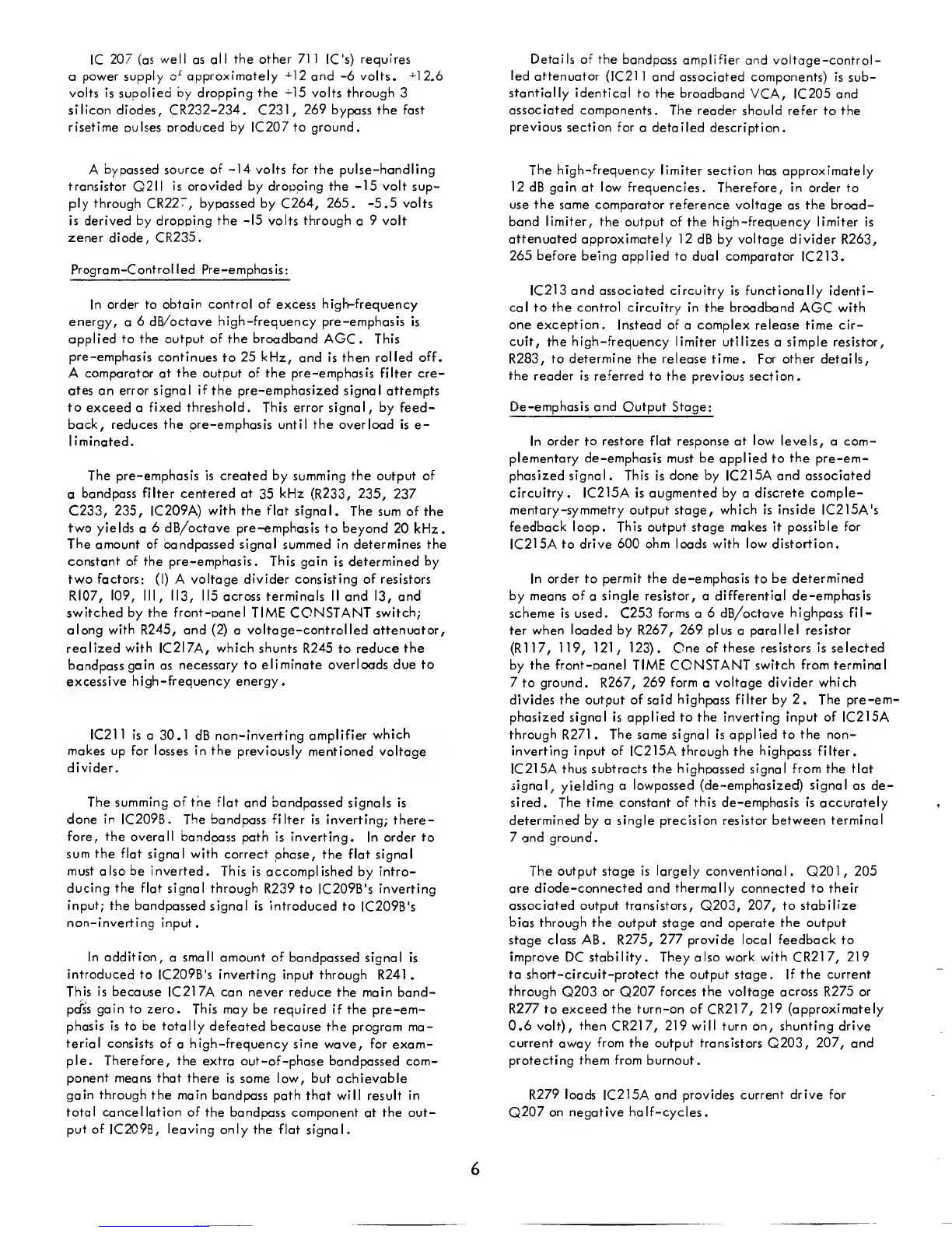
In rack -mounting the 418, very strong AC magnetic
fields should be avoided because these can introduce hum
into the input transformers. In addition, the 418 should
not be mounted directly over equipment producing large
amounts of heat, like vacuumtube power amplifiers.
Ambient temperature should not exceed 45°C (11 3°F
)
when the 418 is powered.
If the 418 is rack-mounted, the jumper on the rear
barrier strip connecting terminal 7(signal ground)
to terminal 8(chassis ground) should be removed to
avoid ground loops. If the 418 is used in aportable situ-
ation, this jumper should be retained in order to assure
that the chassis is grounded. When the jumper is retained,
it is advisable to terminate the line cord with athree-
prong to two-prong AC adapter in order to avoid intro-
ducing ground loops through the AC power line grounding
system. The center (ground) prong on the 418 line cord
(green wire) is connected directly to the chassis.
INSTALLATION: ELECTRICAL
Input;
The input of the 41 8A is a100K ohm balanced bridging
input. It is synthesized by means of an electronic differ-
ential amplifier; no transformer is used. Absolute input
clipping occurs at +21 dBm; higher levels require use of an
external balanced pad. With the INPUT ATTEN full clock-
wise, -10 dBm will produce 10 dB gain reduction.
It is important that both (+) and (-) inputs be driven
by asource impedance of 600 ohms or less in order to
assure best "common mode rejection" (i.e., ground loop
hum rejection). If the device driving the 41 8A has a
balanced output, the two output leads should be driven
directly into the (+) and (-) inputs of the 41 8A. If the
device driving the 41 8A has an unbalanced output, it
snould also be connected to the 41 8A with atwo conductor
shielded cable. The black wire should be connected bet-
ween the driving device's signal ground and the 418A's
(-) input. The second wire should be connected between
the driving device's output and the 418A's (+) input.
This arrangement takes maximum advantage of the hum-
reducing ability of the 418 A's balanced input. In either
case, the shield of the interconnecting cable should be
connected to chassis ground at one end only.
No special RF suppression techniques have been used
in the 418A. If RF interference is experienced in high RF
fields, we suggest bypassing audio inputs, outputs, and the
power line to chassis ground through 0.001 mfd ceramic
capacitors with short as possible leads. Be sure that the
voltage rating of the power line bypass capacitor is at least
1.6 kV, and that bypassing occurs after the fuse to avoid
apotential fire should the capacitor short .Because the
chassis metalwork has not been designed to be rigorously
RF-tight, it is unlikely that the 418A could be operated
immediately adjacent to atransmitter. In abroadcast
production studio, sufficient RF suppression usually exists
so that successful operation can be easily obtained.
Output:
The output of the 418 is unbalanced, and follows the
OUTPUT ATTEN control, which is configured as astandard
potentiometer. Maximum output resistance occurs with
this control at 12 o'clock; in this case, the output resis-
tance is approximately 400 ohms. Maximum available
level is +1 3.4 dBm
.

The output may be used to drive either balanced or
unbalanced-and-floating inputs of external equipment.
Athree conductor shielded cable should be used, with
the inner conductors connected to the 418 output and
signal ground, and the shield terminated to the 418 chassis
ground, and unterminated at the other end. The comments
concerning ground loops in INSTALLATION: MECHANICAL
(above), should be noted. In most cases, the balanced
input will provide ground-loop protection if grounding
is effected as described above.
The 418's VU meter, in OUTPUT positions, is connect-
ed to the output of the 418's line amplifier before the
OUTPUT ATTEN control in order to avoid reflecting
meter rectifier distortion into the output. Therefore,
this metering position will not show any adjustments of
the OUTPUT ATTEN control
.
First, the attack time of the 418 is moderate (in the
order of 2or 3milliseconds) .Therefore, fast -rising
waveforms will overshoot at the 418 output. The over-
shoots are sufficiently short so that they can be clipped
by the recording or transmission medium following the
418 without audible ill effects, provided that said media
can themselves clip. Examples of suitable media are
magnetic tape (whose saturation characteristic provides
an ideal "soft" clipping characteristic), and optical
film, which has amuch more sudden clip point, but
which can be clipped without damage to the medium.
On the other hand, disc recording requires absolute
protection in order to avoid overcutting and/or cutter
lift. Therefore, in the case of disc transfer, the 418
should be followed by some sort of absolute protection,
such as aclipper or avery fast limiter.
Power:
The power transformer can be wired for 105-125 VAC
or 210-250 VAC operation, 50 or 60 Hz. The nominal
voltage for which the unit is wired is marked on the
carton. If the unit is wired for 230 volts, awarning tag
is also affixed to the line cord.
To change line voltage, remove the top cover to re-
veal the power transformer. For 115 volt operation,
connect terminal 1to terminal 2, and terminal 3to
terminal 4(See figure 1).For 230 volt operation,
connect terminal 2 to terminal 3. When altering the
position of the jumpers, take great care not to overheat
or bend terminals or the power transformer may be
damaged. Do not rearrange the insulated wiring.
a.Power transformer
wired for 115 volts
b.Power transformer
wired for 230 volts
Figure 1: Power transformer wiring
If the 418 is to be used in asituation where ground
loops may be introduced through the power line, an al-
ternative to fitting athree-prong to two-prong adapter
on the AC line plug is to disconnect the green wire
emerging from the line cord inside the chassis. However,
be sure that the chassis is grounded through one (and
only one) path when the 418 is installed.
The second important consideration is the fact that the
gain reduction capability of the broadband AGC section
of the 418 has been purposely limited to 15dB.This
was done to obtain amaximally smooth characteristic
from the FET attenuator, and also to assure that excessive
compression (with accompanying unpleasant side-effects)
cannot be used. It is therefore essential to choose the
input operating level with acertain degree of care, com-
pared with operation of compressors capable of, say, 30
dB compression. This care can only result in better-
sounding product, and we therefore consider it adistinct
advantage.
If attempts are made to exceed the permissible AGC
gain reduction range, the front -panel overload lamp will
light. Simultaneously, abrief dropout of high-frequency
content will be noted, because the AGC output will
overshoot dramatically and force the high-frequency limi-
ter into maximum de-emphasis. These conditions are
easily avoided by use of the GAIN REDUCTION metering
position, which will clearly indicate when apotential
overload situation exists.
Third, both INPUT and OUTPUT attenuators are stereo-
ganged controls. They were configured this way in order
to maximize the speed with which adjustments could be
made without concern over unbalancing the stereo channels.
However, this means that initial channel balance must be
done on the equipment driving the 418.
Lastly, the 418 is not two limiters, but rather astereo
device utilizing asingle control loop for both channels.
The gains of the two channels are forced to track each
other, and the amount of gain reduction is determined by
the louder channel at any given moment. This means that
the two channels of the 418 cannot be used for two inde-
pendent program sources; if the 418 is to process mono
material, either channel may be used, with the other
channel carrying no signal.
OPERATING CONSIDERATIONS
In order to use the 418 most successfully, some under-
standing of its particular operating characteristics is
required.
There is at least one specialized use for this facility:
if adisc jockey wishes to have voice-actuated "ducking 1
of music while doing production, one channel of the 418
can carry his voice, while the other channel can carry
music at alower level. Automatic ducking of the music
2

by voice can occur to whatever degree desired by adjust-
ing how hard the voice drives the 418 (and thus, the re-
sulting degree of gain reduction obtained) .
OPERATING INSTRUCTIONS
Connect the 418 to asource of AC power correspond-
ing to the voltage for which the power transformer is
strapped (see INSTALLATION: ELECTRICAL above).
Turn the AC POWER switch ON. The neon pilot lamp
should glow. All metering positions should read zero,
except for GAIN REDUCTION (100% with no signal),
and +15 and -15 monitor the positive and negative
regulated power supplies respectively, and verify that
these are working properly.
The LIN and RIN positions monitor the input levels
after the input "active transformer" differential amplifier,
but before the input attenuator. This position is princi-
pally useful in verifying whether signal exists on the in-
put line, and if so the approximate signal level. "O" VU
on the meter corresponds to approximately +4 dBm (into
600 ohms )equivalent input level.
The LOUT and RCUT positions monitor the output
before the output attenuator.
The G/R (GAIN REDUCTION) position indicates
the approximate amount of broadband gain reduction in
dB.
The amount of gain reduction is determined by the
input level being presented to the limiter; this can be
affected by the drive level to the 418, and also by the
418's INPUT ATTEN control. As this control is turned
clockwise, the amount of gain reduction will increase.
If the operator attempts to exceed approximately 15 dB
gain reduction, the red OVERLOAD lamp will light, and
distortion and severe high-frequency loss may be per-
ceived .
The RELEASE TIME control is not arelease time con-
trol in the classic sense, because automatic circuits in-
side the 418 are constantly analyzing the program mate-
rial and continuously varying the release time to mini-
mize audible limiting "action". The function of the RE-
LEASE TIME control is to adjust the speed of this entire
process. As the release time is speeded up (control to-
wards "fast"), the 418 will increase the average level
("density") of the program to agreater and greater ex-
tent. As the RELEASE TIME control is moved into the
last quarter of its range towards "fast", there is greater
and greater danger that the limiting process will produce
objectionable results. In general, it is desirable to use
less than 6dB gain reduction when operating with such
fast release times. As the release time is slowed down,
more and more gain reduction can be used without signi-
ficant audible side-effects. Slower release times are
particularly useful for "gain riding" functions, such as
mixing through the limiter, where no change in the qual -
ity of the sound is desired, but rather protection from
excessive level which would tend to overload the follow-
ing recording medium is wanted. The automatic release
time adjustments assure that heavy transients (like kick
drum) do not knock "holes" in the audio, while simulta-
neously instruments like French horn or strings do not
"pump". Slower release times are also useful for prepar-
ing masters for cassette duplication, where acceptable
signal-to-noise ratios must be obtained by acertain
amount of compression of the master.
Most recording media (with the exception of 15 and
30 ips tape) are significantly more subject to overload
at high frequencies than at low frequencies, due to the
application of record pre-emphasis. Cassettes are par-
ticularly problematical. The high-frequency limiter in
the 418 can be switched in to automatically control the
high-frequency content of the audio so as to avoid audi-
ble high-frequency overload and accompanying distor-
tion. The four "time constants" do not refer to attack or
release times (which are not adjustable), but rather to
the frequencies at which the control threshold is 3dB
below the broadband (low frequency) threshold. The
following table gives these frequencies, as well as sug-
gested uses for each time constant:
25 uS 6.37 kHz 15 ips tape
37.5 uS 4.24 kHz 7-1/2 ips tape (modern oxide);
RIAA disc (allowing 6dB
headroom)
50 uS 3.18 kHz 3-3/4 ips tape; 7-1/2 ips
broadcast tape cartridge
75 uS 2.12 kHz 1-7/8 ips tape; cassette;
optical film; RIAA disc (al-
lowing no high-frequency
headroom)
It should be noted that more high frequency content
may always be recorded on agiven medium by reducing
the low frequency level, thus allowing more headroom
for high-frequency pre-emphasis. In some cases, this
may be adesirable expedient to achieve abrighter
sound. In other cases, the loss of signal-to-noise ratio
may be intolerable. If the former expedient is adopted,
the high-frequency limiter may be s'Bt on ahigher fre-
quency time constant than normal, thus reducing the
amount of high-frequency limiting. Because of the com-
plex nature of high-frequency overload distortion, the
ear should always be the final arbiter of the proper set-
ting of the TIME CONSTANT control
.
Further details of 418 operation are largely dependent
upon the sound and effect desired from the device. Ex-
perimentation in actual use situations is the best way to
develop aknowledge of the 418's usefulness as well as
its limitations
.
MAINTENANCE
Preventive Maintenance:
The 418 is an entirely solid-state device. The only
preventive maintenance required is keeping the unit
clean. Dust on the circuit board can absorb moisture.
3

causing high-resistance short-circuits and erratic opera-
tion. The front panel should be periodically cleaned;
use of astrong household detergent will usually do an
adequate job without danger of damaging paint, screen-
ing, or plastic parts.
In time, operation of the pots and/or rotary switch
may become erratic because of wear, corrosion, or dirt
build-up. These units are not hermetically sealed, and
may be cleaned with commercial spray-type contact
cleaner. Avoid letting excess cleaner drip onto parts
other than those being serviced.
The electronics are stable indefinitely, and require
no periodic alignment. Alignment instructions have been
included as Appendix Aprimarily for reference. Align-
ment should not be attempted unless the service facility
has the necessary specified test equipment, and the tech-
nician is highly skilled and experienced in the mainte-
nance of equipment employing IC's.
Corrective Maintenance —AGeneral Note:
The 418 employs advanced and sophisticated circuit
techniques based largely upon linear integrated circuit
technology. In case of failure, it is highly advised that
repairs be performed at the factory, in order to take ad-
vantage of the factory technicians' experience and stock
of correct spare parts. Field repairs should only be at-
tempted if the technician is highly experienced and com-
petent in the field of linear integrated circuits, and is
skilled in the fine art of working on double-sided PC
boards with plated-through holes (see following section).
In most cases, failed 1C opamps or comparators may be
replaced without realignment. Flowever, other parts will
often affect alignment. This is particularly true of the
quad-FET arrays and associated components.
In addition, anumber of tight -tolerance parts are
used. These must be replaced by exact equivalents, or
circuit performance will suffer.
SERVICE NOTE: It is usually more economic to
return the 418 to the factory for repair, unless your house
technicians are extremely familiar with the unit, and an
adequate stock of spare parts is on hand.
Replacement of Components in Printed Circuit Boards:
Most circuit boards used in the 418 are of the double-
sided plated-through variety. This means that there are
traces on both sides of the board and that the through-
holes contain ametallic plating in order to conduct cur-
rent through the board. Because of the plated-through
holes, solder often creeps 1/16" up into the hole requir-
ing amore sophisticated technique for component remov-
al in order to prevent serious damage to the traces on
the board. In particular, excessive heating of apoint on
the board will almost always cause damage.
If the user is not thoroughly familiar with elegant
techniques of removing components from double-sided
boards, it is wiser to cut each of the leads of an offend-
ing component from the body while the leads are still
soldered into the board. The body is then discarded and
each of the leads is heated independently and pulled out
of the hole with apair of long nose pliers. Each hole
may then be cleared of solder by carefully heating with a
low wattage iron and sucking the residual solder with a
spring activated solder vacuum tool
.
The new component should be installed in the usual
way and soldered from the bottom side of the board. If
no damage has been done to the plated-through hole,
soldering of the topside pad is not necessary. However,
if the removal procedure did not progress smoothly it
would be prudent to solder each lead carefully at the
topside as well in order to avoid potential intermittent
problems.
After soldering, the residual flux should be removed
with acotton swab moistened with asolvent such as
1,1,1 trichloroethane, naphtha, or 99% isopropyl alco-
hol. These first two solvents are often available in su-
permarkets marketed under the brand name "Energine"
fire-proof spot remover and regular spot remover, respec-
tively. The alcohol, which is less effective, is usually
available in drug stores. Note: Rubbing alcohol is high-
ly diluted with water and is not effective. There are al-
so other solvents marketed under various trade names
which contain Freon .These are often available in
electronic supply houses and are also useful.
It is good policy to make sure that this defluxing oper-
ation has actually removed the flux and not just smeared
it about so that it is less visible. While rosin flux is not
corrosive normally, it can absorb moisture and become
conductive enough to cause severe deterioration in spec-
ifications over time.
Comments on 1C Opamps:
1C opamps are operated in such away that their trans-
fer characteristics are essentially independent of 1C char-
acteristics and dependent only on external feedback com-
ponents. The feedback forces the voltage of the (-) input
terminal to be very close to the voltage at the (+) input
terminal. Therefore, if the technician measures more
than afew millivolts difference between these terminals,
the 1C is probably bad.
Exceptions are IC's used open-loop as comparators,
and IC's whose outputs have been saturated in one direc-
tion or the other due to abnormal inputs. However, if
the technician measures that the (t) input is more posi-
tive than the (-) input, yet the output of the 1C is sitting
at -14 volts, this almost surely indicates 1C failure. If
all the above polarities are reversed, the same thing
holds
.
Because the characteristics of the 418 are essentially
independent of 1C opamp characteristics, an 1C opamp
can usually be replaced with no change in performance.
Adefective opamp may appear to work, yet have ex-
treme temperature sensitivity of DC characteristics. If
parameters appear to drift excessively with temperature.
4

use acan of freeze-spray to locate the offending com-
ponent. Freeze-spray is also very useful in tracking
down intermittents
.
CIRCUIT DESCRIPTION (WITH TROUBLESHOOTING
HINTS):
General
:
The 418 is divided into four major blocks. In order of
signal passage these are:
1) The input buffer and broadband AGC;
2) The program-controlled pre-emphasis, which serves
as ahigh-frequency limiter;
3) The de -emphasis and output stage; and
4) The power supply.
Left and right audio paths are identical, and share a
common control circuit. Only the left channel, plus the
control circuit will be described.
Input Buffer and Broadband AGC:
The signal enters the 41 8A in balanced form, and is
applied to IC201, an LF356 low-noise FET-input opamp
configured as again-of-one differential amplifier. When
both (+) and (-) inputs are driven from source impedances
very small compared to 50K (such as 600 ohms), the am-
plifier is essentially insensitive to signal components that
appear equally on both (+) and (-) inputs (such as hum),
and responds with full unity gain to the difference bet-
ween the (+) and (-) input. Thus it serves as an "active
transformer.
"
If signals in excess of +21 dBm are applied to the input,
this amplifier will clip regardless of the setting of the in-
put attenuator, and an external balanced loss pad must be
employed before the 41 8A input.
The gain control element is aP-channel junction field
effect transistor, IC2I6A, operated as avoltage variable
resistor. This FET shunts the lower leg of the voltage di-
vider R213, 223 to reduce the gain. Note that the va-
lues of R213 and R223 are selected at the factory to com-
plement the particular FET employed. If IC216 is ever
replaced (a highly unlikely occurrence), the factory
should be consulted.
The audio level across the FET is 16 mv at the thresh-
old of limiting. This level is amplified back up by IC205,
a709 opamp configured for 34.5 dB non-inverting gain.
IC205 is frequency-compensated by C2I3, 217, 219 and
R215, 217. The output of IC205 is clamped to +2.4
volts by the diode strings CR20I, 203, 205, 207, 209,
211, 213, 215 to prevent damage to 1C 207 in the event
that excessive input signal is applied. The gain of IC205
is determined by R219, 221, and C225. R229 forces a
constant current to flow from the output of IC205 to the
-15 supply, thus forcing the output stage of IC205 to
operate class Ato eliminate crossover distortion.
The output of IC205 is applied to the two halves of
IC207, a711 dual comparator. The inputs of IC207 also
receive reference voltages of +and -1 .2 volts derived
from voltage dividers R294-297. If the peak level of
the output of' IC205 attempts to exceed +1 .2 volts,
1C 20 7 turns on, producing apulse which is coupled
through C266 and CR228 to Q21 1.Q21 1is turned on
by the pulse, and discharges C267 and C268 through
CR230 and CR229 respectively. This voltage change
across C267 is coupled to the gate of the FET through
R231 ,thereby decreasing the resistance of the FET and
decreasing the gain of the circuit until the overload at
the output of IC205 is removed. Attack time of the cir-
cuit is determined by R288 and is about 2ms. The re-
lease time is avery complex function of the nature of
the program, and is determined by the proprietary cir-
cuit inside the module. Basically, the module derives
avoltage based on the previous history of the program
and applies the voltage to one end of the RELEASE TIME
control, P211. The other end of P211 is connected to
C268, and permits C268 to charge at arate controlled
by the module in conjunction with the setting of P211.
In addition, the network CR231 and R289 provides de-
layed release to assure low distortion at low frequencies.
This is accomplished as follows:
When gain reduction occurs, both C267 and C268 are
discharged to the same voltage because CR230 and CR229
have substantially identical voltage drops. However,
C267 must charge (release) through CR231 and R289.
R289 provides virtually no short-term release because of
its high value. Therefore, C267 cannot charge until
C268 has charged sufficiently to overcome the turn-on
voltage of CR231 .This time delay eliminates the usual
sawtooth ripple on the control voltage, thus drastically
reducing distortion.
The collector of Q211 is clamped to ground through
the base-emitter junction of Q210. This way, the gate
of the control FET cannot be forward-biased. In addi-
tion, when Q210 conducts, it turns on the front -panel
OVERLOAD LED, thus indicating that the permissable
15 dB gain reduction range has been exceeded.
P210 determines the quiescent gate voltage of the
control FET, and is adjusted to pinch this FET off when
no gain reduction occurs. Thus maximum gain is extre-
mely stable, and no distortion is introduced by the FET.
The control FET is contained in apackage with four
matched, monolithic FET's. The second FET is used to
control the gain of the right channel; the third FET is
operated with DC across it to control the GAIN REDUC-
TION meter. The fourth FET is not used. The DC gain
reduction signal is amplified by IC219, anon-inverting
opamp
.
5

1C 207 (as well as all the other 71 1IC's) requires
apower supply olapproximately +12 and -6 volts. -*-12.6
volts is supplied by dropping the +15 volts through 3
silicon diodes, CR232-234. C231, 269 bypass the fast
risetime oulses produced by IC207 to ground.
Abypassed source of -14 volts for the pulse-handling
transistor Q2II is provided by dropping the -15 volt sup-
ply through CR22 -
,bypassed by C264, 265. -5.5 volts
is derived by dropping the -15 volts through a9volt
zener diode, CR235.
Program-Controlled Pre-emphasis:
In order to obtain control of excess high-frequency
energy, a6dB/octave high-frequency pre-emphasis is
applied to the output of the broadband AGC. This
pre-emphasis continues to 25 kHz, and is then rolled off.
Acomparator at the output of the pre-emphasis filter cre-
ates an error signal if the pre-emphasized signal attempts
to exceed afixed threshold. This error signal, by feed-
back, reduces the pre-emphasis until the overload is e-
Iiminated
.
The pre-emphasis is created by summing the output of
abandpass filter centered at 35 kHz (R233, 235, 237
C233, 235, IC209A) with the flat signal. The sum of the
two yields a6dB/octave pre-emphasis to beyond 20 kHz.
The amount of oandpassed signal summed in determines the
constant of the pre-emphasis. This gain is determined by
two factors: (I) Avoltage divider consisting of resistors
RI07, 109, III, 113, 115 across terminals II and 13, and
switched by the front-panel TIME CONSTANT switch;
along with R245, and (2) avoltage-controlled attenuator,
realized with IC2I7A, which shunts R245 to reduce the
bandpass gain as necessary to eliminate overloads due to
excessive high-frequency energy.
IC211 is a30.1 dB non-inverting amplifier which
makes up for losses in the previously mentioned voltage
divider.
The summing of tne fiat and bandpassed signals is
done in IC209B. The bandpass filter is inverting; there-
fore, the overall bandoass path is inverting. In order to
sum the flat signal with correct phase, the flat signal
must also be inverted. This is accomplished by intro-
ducing the flat signal through R239 to IC209B 's inverting
input; the bandpassed signal is introduced to IC209B's
non-inverting input.
In addition, asmall amount of bandpassed signal is
introduced to IC209B’s inverting input through R241 .
This is because IC217A can never reduce the main band-
pcfss gain to zero. This may be required if the pre-em-
phasis is to be totally defeated because the program ma-
terial consists of ahigh-frequency sine wave, for exam-
ple. Therefore, the extra out-of-phase bandpassed com-
ponent means that there is some low, but achievable
gain through the main bandpass path that will result in
total cancellation of the bandpass component at the out-
put of IC2C9B, leaving only the flat signal.
Details of the bandpass amplifier and voltage-control-
led attenuator (IC21 1and associated components) is sub-
stantially identical to the broadband VCA, IC205 and
associated components. The reader should refer to the
previous section for adetailed description.
The high-frequency limiter section has approximately
12 dB gain at low frequencies. Therefore, in order to
use the same comparator reference voltage as the broad-
band limiter, the output of the high-frequency limiter is
attenuated approximately 12 dB by voltage divider R263,
265 before being applied to dual comparator IC213.
1C 213and associated circuitry is functionally identi-
cal to the control circuitry in the broadband AGC with
one exception. Instead of acomplex release time cir-
cuit, the high-frequency limiter utilizes asimple resistor,
R283, to determine the release time. For other details,
the reader is referred to the previous section.
De-emphasis and Output Stage:
In order to restore flat response at low levels, acom-
plementary de-emphasis must be applied to the pre-em-
phasized signal. This is done by IC215A and associated
circuitry. IC215A is augmented by adiscrete comple-
mentary-symmetry output stage, which is inside IC215A's
feedback loop. This output stage makes it possible for
IC215A to drive 600 ohm loads with low distortion.
In order to permit the de-emphasis to be determined
by means of asingle resistor, adifferential de-emphasis
scheme is used. C253 forms a6dB/octave highpass fil-
ter when loaded by R267, 269 plus aparallel resistor
(R 117, 119, 121, 123). One of these resistors is selected
by the front-panel TIME CONSTANT switch from terminal
7to ground. R267, 269 form avoltage divider which
divides the output of said highpass filter by 2. The pre-em-
phasized signal is applied to the inverting input of IC215A
through R271 .The same signal is applied to the non-
inverting input of IC215A through the highpass filter.
1C 215Athus subtracts the highpassed signal from the flat
signal, yielding alowpassed (de-emphasized) signal as de-
sired. The time constant of this de-emphasis is accurately
determined by asingle precision resistor between terminal
7and ground.
The output stage is largely conventional. Q201 ,205
are diode-connected and thermally connected to their
associated output transistors, Q203, 207, to stabilize
bias through the output stage and operate the output
stage class AB. R275 ,277 provide local feedback to
improve DC stability. They also work with CR217, 219
to short-circuit-protect the output stage. If the current
through Q203 or Q207 forces the voltage across R275 or
R277 to exceed the turn-on of CR217, 219 (approximately
0,6 volt), then CR217, 219 will turn on, shunting drive
current away from the output transistors G203, 207, and
protecting them from burnout.
R279 loads IC215A and provides current drive for
Q207 on negative half-cycles.
6

R273 is the feedback resistor for the operational am-
plifier circuitry including IC215A and its discrete output
stage. The signal is then applied across P21 3providing
variable output attenuation. R125 is acurrent limiting
resistor for the meter.
Power Supply:
The AC enters the chassis and is applied through the
fuse to the power transformer. This transformer may be
strapped for 115 volt or 230 volt operation; instructions
for doing so are found in the INSTALLATION: ELEC-
TRICAL section.
The center-tapped secondary of the power transformer
is applied to two pairs of diodes, CR601-604, operating
as a pair of full-wave rectifiers to derive unregulated
voltages of approximately +22.5 volts DC. The outputs
of the rectifiers are smoothed by energy-storage capaci-
tors C601 ,602
.
Most of the positive regulator is contained in IC601 ,
a723C voltage regulator. IC601 contains astable source
of reference voltage (nominally 7.15 volts), an operation-
al amplifier to compare the output with the reference, a
series pass transistor to drive the external power transistor
Q604, and acurrent-limit transistor. The reference vol-
tage output at pin 6is filtered by C603 to reduce noise
and is introduced to the (+) input of the opamp, pin 5.
The unregulated positive voltage is applied to pins 1
1
and 12, and to the collector of series pass transistor Q604,
operated as an emitter-follower. The output current of
Q604 passes through R601, which develops avoltage drop
proportional to the current through it. This voltage drop
is sensed across pins 2and 3of IC601 .If it exceeds ap-
proximately 0.55 volts, the internal current limit transis-
tor turns on and prevents further increase in output cur-
rent, thus providing short-circuit protection for Q604.
The output is sensed by the voltage divider R602, 603,
P601 ,and is applied to the (-) input of the internal opamp
(pin 4). The voltage divider reduces the output voltage
until it is equal to the reference voltage. The output vol-
tage is therefore held at amultiple of the reference vol-
tage by means of feedback. This multiple (and therefore
the output voltage) is adjusted by means of P601 .C604
frequency-compensates the interna! opamp to prevent
high-frequency oscillations. Further stabilization is pro-
vided by C605 across the output of the regulator.
The -15 supply is generated by means of a741C opamp,
IC602, in conjunction with external transistors. IC602
is connected as an inverting, unity gain amplifier with
input resistor R607 and feedback resistor R606. Thus, the
negative output tracks changes in the positive output.
The positive power supply for IC602 is provided by
IC601 .IC601 contains an internal 6.8 volt zener diode,
which drops the +15.7 volt output of the internal series
pass transistor to approximately +9 volts. This voltage is
available at pin 9. Negative supply voltage for IC602
is provided by the unregulated negative supply. This
scheme assures that the total supply voltage for IC602
can never exceed IC602 's maximum 36 volt rating.
IC602 drives aconjugate emitter follower, Q602,
603, R604. As in the case of the positive supply, the
output current is dropped across R605, and if the voltage
across R605 exceeds approximately 0.55 volts, Q601
turns on and shunts drive current away from Q602, simul-
taneously activating the protective current limiting cir-
cuitry inside IC602 which limits IC602's own output cur-
rent to asafe level
.
FACTORY SERVICE
Factory service is available through the life of the
418 from the address above. During the warranty peri-
od, no charge will be made for parts or labor, subject to
warranty conditions. After expiration of the warranty,
areasonable charge will be made for parts, labor, and
packing. In any event, transportation charges (which
are usually quite nominal) shall fall on the customer.
Before returning any unit for repair, please write or
telephone for instructions, stating the trouble experienced.
Often aproblem can be solved by consultation, saving
everyone the delay, inconvenience, and expense of ac-
tually returning the unit.
SHIPPING INSTRUCTIONS
If the original packing material is available, it should
be employed. Otherwise, a carton of at least 200 lbs
bursting test should be obtained which is no smaller than
22 x15x9 inches.
The assembly should be packed so that there is at
least 1-1/2" of packing material protecting every point.
Cushioning material such as Air-Cap, Bubble-Pak, foam
"popcorn", or fibre blankets are acceptable. Folded
newspaper is not suitable. Blanket-type material
should be tightly wrapped around the assemblies and taped
in place to prevent the unit from shifting out of its pack-
ing and contacting the walls of the carton.
The carton should be packed evenly and fully with the
packing material filling all voids so that the units can-
not shift in the carton. Test for this by closing but not
sealing the carton and shaking vigorously. If the unit can
be heard or felt moving, use more packing.
The carton should be well-sealed with 3" reinforced
sealing tape applied across the top and bottom of the box
in an "H" pattern. Narrower or parcel-post type tapes
will not withstand the stresses applied to commercial ship-
ments.
The package should be marked with the name of the
shipper and the words, in red, DELICATE INSTRUMENTS,
7

FRAGILE! Even so, the freight people will throw the box
around as if it were filled with junk. The survival of the
unit depends almost solely on the care taken in packingl
APPENDIX A: ALIGNMENT INSTRUCTIONS
This section of the manual is included primarily for
purposes of reference, as PERIODIC COMPLETE ALIGN-
MENT IS NOT RECOMMENDED OR NECESSARY. Com-
plete alignment is astep-by-step procedure which assumes
that none of the trimmer controls are correctly adjusted.
IF THE REQUIRED TEST EQUIPMENT IS NOT AVAILABLE,
DO NOT ATTEMPT TO PERFORM COMPLETE ALIGN-
MENT,,
Required Instrumentation:
The following instrumentation is required for complete
alignment:
(1) Audio Sinewave Generator, with less than 0.05%
residual harmonic distortion
(2) Digital Voltmeter, basic DC accuracy 0.1% or better
(3) Audio Voltmeter/Harmonic Distortion Meter with 1
megohm or higher input impedance (e.g. H-P 334A)
(4) Triggered Sweep Oscilloscope with X-Y capability
and minimum 5MHz vertical bandwidth
Setup for Complete Alignment:
Complete alignment must be performed on atest bench
away from strong RF fields. Before commencing align-
ment, apply power and allow 30 minute warmup with cov-
ers in place. Remove the top and bottom covers imme-
diately before starting alignment procedure. ALIGN-
MENT MUST BE PERFORMED SEQUENTIALLY. DO
NOT SKIP STEPS. Alignment points can be found on
page 11
.
Alignment Procedure:
(1) Connect digital voltmeter across C605, and read
voltage.
(2) Adjust P601 for areading of +15.00 volts on DVM.
(3) Jumper chassis and circuit grounds together.
(4) Turn P210 (broadband FET bias) CW until the GAIN
REDUCTION meter indicates that gain reduction is
beginning. Back off P210 until no further change is
noted in GAIN REDUCTION.
(5) Adjust P212 (G/R Meter Cal) until the GAIN REDUC-
TION meter indicates 100%.
(6) Connect oscillator to LEFT AUDIO INPUT. Adjust
oscillator for 5kHz. Adjust INPUT ATTEN to 12
o'clock.
Increase oscillator output until GAIN REDUCTION
meter indicates -8.5 dB
.
(7) Connect oscilloscope to SCOPE OUTPUT of distortion
analyzer. Connect input of distortion analyzer to the
left channel broadband limiter output (terminal 29),
which is afork terminal close to the right rear of the
limiter board when viewed from the front. Operate
distortion analyzer so that the oscilloscope displays
the input to the distortion analyzer (normally the
"SET LEVEL" mode). Operate the scope in NORMAL
TRIGGER mode, and adjust trigger level so scope
barely stops triggering.
(8) Remove the hot lead of the oscillator from LEFT AUDIO
INPUT. Turn the RELEASE TIME control full CCW.
Now reconnect the hot lead of the oscillator, trying
to make aclean reconnect. Observe the scope, which
should trigger on the overshoot produced by the finite
attack time of the broadband limiter. With the scope
time base set at 2ms/cm, adjust P210 (Broadband FET
bias) trimmer for ascope pattern similar to Fig. 2
This pattern will be transient, but should be easily
visible. Fig. 2was photographed using astorage
scope. To repeat the pattern, it is necessary to alter-
nately disconnect and reconnect the hot lead of the
oscil lator.
BROADBAND LIMITER ATTACK
(no signal to 10 dB gain reduction)
(2 mS/cm; IV/cm)
FIGURE 2
(9)
Reconnect the oscillator. Switch frequency to 1kHz,
and reduce the output level until 4dB gain reduction
is observed. Without moving the distortion analyzer
input, measure the harmonic distortion, and adjust
P203 (left distortion null) for minimum THD. Typical
reading will be 0.025% if an 80 kHz lowpass filter is
employed to reduce the effects of out-of-band noise
on the reading
.
(10) Connect the oscillator to the RIGHT AUDIO INPUT,
and follow the instructions of step 9, substituting
P204 (right distortion null), and observing the right
channel broadband limiter output (terminal 31).
(11) Connect the distortion analyzer to pin ^7 of 1C2 10b
.
Increase oscillator frequency to 5kHz; decrease os-
cillator output until GAIN REDUCTION meter just
barely reads 0 dB. Set the front-panel TIME CON-
STANT switch to 75 uS.
8

(12) Operate the distortion analyzer so that the scope
displays the input to the distortion analyzer. Reduce
analyzer sensitivity until no overload occurs. With
scope in NORMAL TRIGGER mode, adjust TRIGGER
LEVEL until sweep barely shuts off.
(13) As you did with the broadband limiter test in step
8, alternately connect and remove the hot lead
from the oscillator, while observing the scope as it
triggers on the overshoot from the high-frequency
limiter. Adjust P209 (high-frequency FET bias) until
the scope displays asingle-shot pattern like FIG. 3
with the scope time base adjusted for 1ms/cm.
HIGH FREQUENCY LIMITER ATTACK
(5 kHz —no signal to 10 dB gain reduction)
(5V/cm; 1mS/cm)
FIGURE 3
(14) Connect the distortion analyzer to fork terminal ^5
(and readjust the oscilloscope triggering so that the
distortion signal can be viewed). Measure the har-
monic distortion. Reduce the level of the oscillator
until the distortion is maximum. Adjust P208 (right
h. f. distortion null) to minimize THD.
(15) Connect the oscillator to the LEFT AUDIO INPUT
and repeat step 14, connecting the distortion ana-
lyzer to the left channel h. f. limiter output (termi-
nal 2), and adjusting P207 (left h. f. distortion null)
for minimum distortion.
This concludes the alignment procedure.
APPENDIX B: SPECIFICATIONS
INPUT:
Impedance: 150 kohms balanced; active differential input.
Level: -10 dBm produces 10 dB gain reduction with jnpjut attenuator fully clockwise.
Absolute input overload occurs at +21 dBm.
OUTPUT:
Impedance: less than 400 ohms, unbalanced.
Level: + 4 dBm nominal with output attenuator full clockwise. Peak level approximately
+12 dBm. y
FREQUENCY RESPONSE:
±0.5 dB, 20-20,000 Hz below high-frequency limiter threshold.
HIGH-FREQUENCY LIMITER:
Controls high-frequency peaks attempting to exceed athreshold defined by asingle-time-
constant rolloff of 75, 50, 37.5, or 25 microseconds, ±3%. Rolloffs are switch selectable
from front panel, and high-frequency limiter is defeated in “flat” position.
Attack Time: approximately 3milliseconds.
Release Time: varies around 15 milliseconds according to program history.
Control Element: junction field-effect transistor
BROADBAND LIMITER:
Attack Time: 1to 2milliseconds.
Release Time: Program-controlled by means of quadruple time-constant release time
analog processor. Release time may be scaled fast or slow by means of continuously
variable Release Time control available to user.
Range of Gain Reduction: greater than 15 dB.
Compression Ratio: in excess of 200:1
Interchannel Tracking: ±1.5 dB max.; 1 1dB typ.
Control Element: junction field-effect transistor
SEPARATION:
50 dB or better, 20-20,000 Hz.
NOISE (dB below limiting threshold at 100 Hz; 20-20,000 Hz bandwidth):
-80 dB typ.; -75 dB max.
TOTAL HARMONIC DISTORTION: (See graph)
Ibtai Harmonic Dmortion (<M>)
OPERATING CONTROLS:
OUTPUT ATTENUATOR (left and right ganged)
INPUT ATTENUATOR (left and right ganged)
RELEASE TIME
H-F LIMITER TIME CONSTANT
75 uS; 50 uS; 37.5 uS; 25 uS; flat
METER SELECTOR
left input; right input; left output; right output; gain reduction; -f 15 volt power supply;
-15 volt power supply
AC UNE OFF/ON
INDICATORS:
AC POWER PILOT LAMP
OVERLOAD (tights if attempt is made to exceed possible broadband AGC range)
METER [3.5” (8.9 cm) with VU “A” scale and characteristics]
POWER REQUIREMENT:
115/230 VAC ±10 %; 50-60 Hz, approximately 6watts. U-ground power cord attached.
DIMENSIONS:
19" (48.3 cm) wide x3.5" (8.9 cm) high x10” (25.4 cm) deep.
OPERATING TEMPERATURE RANGE:
0-50° C.
WARRANTY:
1year, parts and labor. Subject to limitations set forth in our standard warranty agreement.
9

BROADBAND AGC
I
Orban
Associates
Inc.
TITLE:
LIMITER BLOCK DIAGRAM
MODEL 418A

Orban
Associates
Inc.
TITLE:
’~
15V BIPOLAR POWER SUPPLY
MODEL 41 8A
600 18-000-02 ©1980
NvOUNTEP ON CHASMS MOUNTE-P ON PC&
R6pOa,lSK,l'& .-I5V
500R.C.E

HIGH FREQUENCY LIMITER OUTPUT
AJk Ji »*!i
P207
LEFT
HIGH FREQUENCY
DISTORTION NULL tea
ri ri OC3,000c
~2C145 XC245 2c~ICZH I
°r^^0W*OfK¥
step '»« =
ItaBe o0og
JiG^taD-O ooe
Pocrag-o ||
Ilf
e$i£§:
hc|« otl3
P208
RIGHT
HIGH FREQUENCY
DISTORTION NULL
TIC 2,0 p»bkiM
P209
HIGH FREQUENCY
FET BIAS
i
C605
+15 VOLT
TEST POINT BROADBAND LIMITER OUTPUT
LEFT I1right
l» 10 21 22 fej 24 25
!><§)# -0-
Li ^i? 321 ?? EL 31 33 3«33
P203
LEFT
DISTORTION
NULL
lailillHllsiisiiig ogjoMHofcjc
imii-Q P2QB roj/maT
«HQ-ejO O•
RZ27 U
P204
-iH.3°F€ OO
4R22S Y-P 0>
f00 o?l
Giliill-O G-dlEl-O OOI|I 1aX|VJ of
P2i 22
Illlllllll T^pl^^^^lp5600
~°|J|
i^OO o
o*’ O
RClEASf TIME
MODULE
OO o,
OOOOO O
OOO000
I®ooo ooo ooo
® ©
P204
RIGHT
DISTORTION
NULL
P212
GAIN REDUCTION
METER CALIBRATE
P60I
+15 VOLT
TRIM
P210
BROADBAND
FET BIAS
Orban
Associates
Inc.
LIMITER ASSY DWG
MODEL 4I8A
30080-003-10©! 980

ZZOfS
60008
-
003
-
09
©1980
Table of contents
Other Orban Stereo System manuals