Pentium HOT-541 User manual

User's Manual 1
HOT-541
Pentium PCI MAIN BOARD
User's Manual

2 User's Manual
NOTICE
Copyright 1995.
All Right Reserved
Manual Ver 2.0 ( for 541V2.0, 2.1, 2.2)
All information, documentation, and specifications contained in this manual are subject to change
without prior notification by the manufacturer.
The author assumes no responsibility for any errors or omissions which may appear in this docu-
ment nor does it make a commitment to update the information contained herein.
TRADEMARKS
Intel is a registered trademark of Intel Corporation
PC/AT is a registered trademark of International Business Machine Corporation.
OS/2 is a registered trademark of IBM Corporation.
All other brand and product names referred to in this manual are trademarks or registered trade-
marks of their respective holders.

User's Manual 3
TABLE OF CONTENTS
PREFACE................................................................................... 5
CHAPTER 1 INTRODUCTION........................................................ 6
Specification ............................................................................................ 6
541 Mainboard Description ................................................................... 8
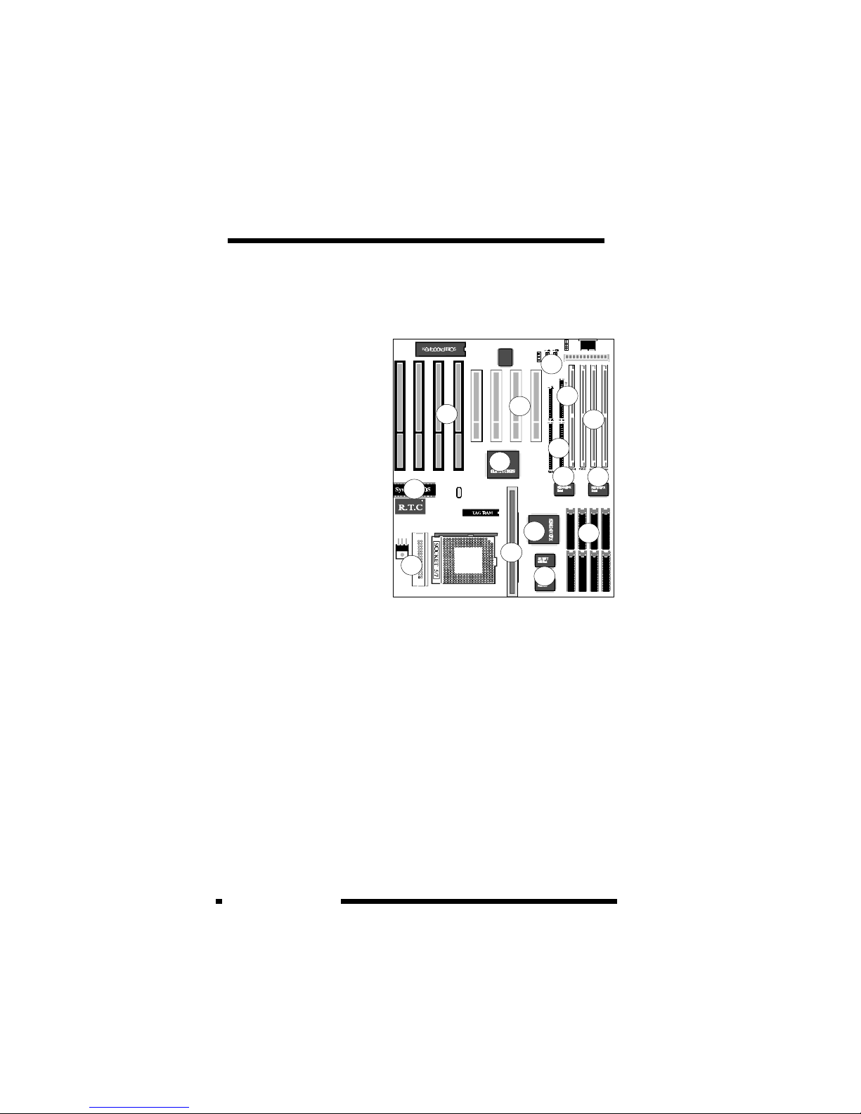
541 Mainboard Layout .........................................................................10
CHAPTER 2 JUMPER SETTING ....................................................11
System Clock Selection .........................................................................11
Pentium CPU Clock Multiplier..............................................................12
Onboard Regulator & VRM Selection...................................................13
Onboard Voltage Regulator Output Selection .....................................14
AT Bus Clock Selection .........................................................................15
Cache Type Selection............................................................................16
Standard Type Cache Size Selection ....................................................18
Cache Voltage Selection........................................................................19
I/O Port Setting & Parallel Port DREQ Selection ...................................20
Flash EPROM Jumper ............................................................................21
Clear CMOS...........................................................................................22
Clear Password ......................................................................................22
Connectors ............................................................................................23
CHAPTER 3 MEMORY CONFIGURATION......................................26
Memory Configuration Reference Table...............................................27
Chapter 4 Power management..............................................................28
Power Management Description ..........................................................28
EPMI Connector ....................................................................................29
CHAPTER 5 AMI BIOS SETUP ...................................................30
BIOS Setup Feature................................................................................31
Navigating with the keyboard in WinBIOS Setup.................................32
Standard Setup.......................................................................................34
Advanced Setup ....................................................................................36
Chipset Setup.........................................................................................40
Power Management Setup ....................................................................43
Peripheral Setup ....................................................................................45
WinBIOS Password Support .................................................................47

4 User's Manual
CHAPTER 6 AWARD BIOS SETUP ..............................................49
Entering Setup........................................................................................49
Using Control Keys................................................................................50
The Main Menu.....................................................................................51
Standard CMOS Setup ..........................................................................53
BIOS Features Setup ..............................................................................57
Chipset Features Setup ..........................................................................60
Power Management Setup ....................................................................64
PCI Configuration Setup........................................................................67
Password Setting....................................................................................69
IDE HDD Auto Detection ......................................................................70
APPENDIX A AMI BIOS REFERENCE .........................................73
APPENDIX B AWARD BIOS REFERENCE .....................................74

User's Manual 5
HOT-541 mainboard is a highly integrated IBM PC/AT compatible system
board. The design will accept Pentium processors operating in 75MHz,
90MHz, 100MHz, 120MHz, and 133MHz, and also features high-perfor-
mance asynchronous and pipelined burst secondary cache memory support
with size of 256KB and 512KB. The memory subsystem is designed to sup-
port up to 128 MB of EDO RAM or standard Fast Page DRAM in standard 72-
pin SIMM socket. A type 5 or type 7 Pentium CPU socket provides access to
future processor enhancements.
HOT-541 provides a new level of I/O integration. Intel's T-Chip 82430 PCISet
chip set provides increased integration and improved performance over other
chip set designs. The T-Chip chipset provides an integrated Bus Mastering
IDE controller with two high performance IDE interfaces for up to four IDE
devices.
The SMC Super I/O controller provides the standard PC I/O functions: floppy
interface, two FIFO serial ports, one SPP/EPP/ECP capable parallel port.
Up to four PCI local bus slots provide a high bandwidth data path for data-
movement intensive functions such as graphics, and up to four ISA slots com-
plete the I/O function.
The HOT-541 provides the foundation for cost effective, high performance,
highly expandable platforms, which deliver the latest in Pentium processor
and I/O standard
Preface

6 User's Manual
Chapter1 Introduction
Specification
CPU Function
CPU clock: 75/90/100/120/133 MHz
Fully supports Intel's 3.3V Pentium processors
Optional VRM socket for Intel's future P55C processors
Chipset
Intel T-Chip PCISet 82437FX, 82438FX, and 82371FB
Memory
Supports two banks of EDO RAM and Fast Page DRAM
ranging from 8MB to 128MB
Supports 1M x 32 (4MB), 2M x 32 (8MB), 4M x 32(16MB),
and 8M x 32 (32MB) 72-pins SIMMs
Cache Memory
Integrated L2 write-back cache controller
- Pipelined Burst or standard SRAM
- 256KB or 512KB Direct Mapped
Power Management Function
Provides four power management modes : Full on,
Standby, and Suspend
Supports Microsoft APM
Provides EPMI (External Power Management Interrupt)
pin

User's Manual 7
Expansions
32-bit PCI bus slot x 4
16-bit ISA bus slot x 4
2-channel PCI IDE port
- Support up to 4 IDE devices
- PIO Mode 4 transfers up to 16 MB/sec
- Integrated 8 x 32-bit buffer for PCI IDE burst transfers
One floppy port
One parallel port
- Supports SPP (PS/2 compatible bidirectional Parallel
Port), EPP (Extended Parallel Port), and ECP (Extended
Capabilities Port) high performance parallel port.
Two serial ports
- Supports 16C550 compatible UARTS.
One or two PS/2 mouse ports
Board Design
Dimension 22cm x 28cm

8 User's Manual
541MainboardDescription
4
5
6
8
9
10
Themajorcomponentsof
541 mainboard are illus-
tratedanddescribedright
andbelow. Please takea
minutetobecomefamiliar
withtheboarddesign.
1. ChipsetASIC
541mainboardisdesigned
arounda setof highlyinte-
gratedIntelT-ChipPCISet,
whichoffersoptimumper-
formanceonPCI and ISA
base system for a cache
controller, a local DRAM
controller, and an inte-
gratedPeripheralscontrol-
ler.
2.SystemMicroprocessor
541 mainboard accept member of the 3.3V Pentium family and future
P55C high performance 64-bit microprocessors in PGA package. The
mainboardis designedtorun ataclock speedfrom 50 to66MHz onCPU
bus clock, and 75 to 133 MHz on CPU core clock.
3.SecondaryCacheArchitecture
541 maniboard support pipelined burst or standard SRAM on external
cachememory with sizeof 256KBor512KB, andaCard EdgeLow Profile
(CELP)socket provides flexibilityforcache module options.
4.MemoryArchitecture
541 mainboard features four 72-pin SIMM (Single In-line Memory Mod-
ule)sockets organizedinto twobanks,which allowflexible memorycon-
figuration and expansion. It may use 4MB, 8MB, 16MB and 32MB EDO
orFast Page SIMMstoexpand memory from8MB to 128MB.
11
1
1
1 1
3
3
3
2
7

User's Manual 9
5.PCIExpansionSlots
541 mainboard provides four 32-bit PCI expansion slots, which may
accommodatemany third-partyexpansion cardsand increaseflexibility
indesigningcustomplatforms.
6.ISAExpansionSlots
541 mainboard provides four 16-bit ISA expansion slots, which may
accommodatemany third-partyexpansioncards andenormousflexibil-
ityin designingcustomplatforms.
7.VoltageRegulator&VRM
Theon-boardvoltregulatororVRM(VoltageRegulator Module)provides
powerfor thePentium process,PCISet andsecondary cache.It provides
3.3V range for Pentium P54C family and 3.3V/2.5V for P55C.
8.On-boardPCIIDEController
541 mainboard provides a on-board 2-channel IDE controller with high
speeddata transferrate. Itsupportup tofour IDEdevices.
9.On-boardFloppyController
541mainboardprovidesaon-boardfloppycontrollerthatsupport360KB,
1.2MB, 720KB, 1.44MB, and 2.88MB type floppy disk drives.
10.On-boardSerial/ParallelPort
541 mainboard provides two serial (COM) ports and one parallel port.
11.SystemBIOS
541mainboardprovides licensed AMI WinBIOSorAward system BIOS
which are particularly designed to offer optimise performance of the
mainboard.
12.AttachedAccessories
one40-pinhard disk driveflatcable
one 34-pin floppy disk drive flat cable
one9-pin and25-pinserial connectorwithcable
one25-pinparallel port connectorwithcable

10 User's Manual
541MainboardLayout

User's Manual 11
Chapter2JumperSetting
SystemClockSelection
541mainboardfeaturesaclockgen-
eratortoprovideadjustablesystem
clockfrequency. JP15andJP16are
2-pin jumpers which determine the
systemclockfrequency.
Properjumper settingsforgenerat-
ing 50MHz to 66MHz clock fre-
quency for Pentium system are
shown bellow.
50MHzSystemClock 60MHzSystemClock
66MHzSystemClock

12 User's Manual
PentiumCPU ClockMultiplier
2 : 3
50 / 75
2 : 3
50 / 75
60 / 90 60 / 90
66 / 100 66 / 100
1 : 2
50 / 100
1 : 2
50 / 100
60 / 120 60 / 120
66 / 132 66 / 132
1 : 3
50 / 150
1 : 3
50 / 150
60 / 180 60 / 180
2 : 5
60 / 150
2 : 5
60 / 150
66 / 166 66 / 166
541 mainboard provides JP3
andJP58tofigureupPentium
CPUcore clockmultiplier. By
insertingorremoving jumper
capsonJP3andJP58,theuser
can change the Host Bus
Clock/CPU Core Clock ratio
from 1 : 1.5 to 1 : 3.

User's Manual 13
Onboardregulator &VRMSelection
541 mainboard is designed an onboard
voltageregulator to provide3.3V ranger for
pentium(P54C) and a optional VRM (Volt-
age Regulator Module) to offer 3.3V/2.5V
rangerforfutureP55Cprocessors.
ForP55Cprocessors, theyneedtwo voltage
level, 3.3V for CPU I/O and 2.5V for CPU
core.
Nomarlly,VRMsupports both voltage level
, but some particular VRM, they only pro-
vide2.5Vand require onboardregulatorto
complement 3.3V to P55C.

14 User's Manual
OnboardVoltageRegulator OutputSelection
541mainboard isdesigned toof-
ferseveralCPU voltageslevelfor
Pentium(P54C) family require-
ments. 3.3V for standard 75/90/
100/120/133MHz Pentium pro-
cessor, 3.45V for VR s-spec
Pentium processor (3.3V +5% -
0%), and 3.6V for VRE s-spec
Pentiumprocessor(3.45Vto3.6V).

User's Manual 15
ATBusClockSelection
541mainboardprovidesajumper
JP18to set theATbus (ISA bus)
clock that divide from system
clock, the available settings are
SCLK/6andSCLK/8.
Pleasereferthe followtableto set
theATbusclock.
Note:8MHzATbusclockisrec-
ommended.

16 User's Manual
CacheTypeSelection
OnboardStandardCache
RAM
CELPsocketforCache
Module
Onboardstandardasynchronouscache
541 mainboard provides 9 pcs DIP socket to accommodate standard
asynchronous cache, with default size of 256KB and upgradable to
512KB.(pleaserefertosectionof"StandardTypeCacheSelection ")
Standardasynchronouscachemodule
541mainboard provides oneCELP ( CardEdge Low Profile) socket to
accommodate256KBstandardasynchronouscachemodule.(Thesame
CELPsocketalsoaccommodatepipelinedburstcache module)
541mainboard supportseveraltypes cachescheme includingonboard
standardasynchronouscacheRAM,standardasynchronouscachemod-
ule, onboard pipelined burst cache SRAM, and pipelined burst cache
module.
OnboardPipelinedBurst
CacheRAM

User's Manual 17
OnboardpipelinedburstcacheRAM
Afactory optionon 541mainboardis anintegrated 256KBexternal cache
implementedwith two 32Kx32 pipelined burstSRAM devices soldered
tothe mainboard.A 5v32KBx8external TagSRAM isrequired.
PipelinedBurstcachemodule
IftheHOT-541 isorderedwith nocacheinstalled,thecachecanbeadded
laterina field upgradebyinstalling a pipelined burstcache module into
thesocket. TheCELPsocketcanaccommodate256KBcachemodules.

18 User's Manual
StandardTypeCacheSizeSelection
Note : AllDataSRAM mustbemixedmode,and TagSRAM mustbe 5V.
AllofData and TagSRAM must with aspeed of 15ns orfaster.
256KB CacheMemory
256KB 32K x 8 32K x 8
512KB CacheMemory
512KB 64K x 8 32K x 8
541mainboardsupportsstandard
typeextendedcachememorysizes
of 256KB and 512KB. Cache
memoryisrealized by eight Data
SRAM and one Tag SRAM. The
512KB configuration uses eight
64KB x 8 SRAM, each of SRAM
fillstheentire socket. The256KB
configurationuseseight 32KB x 8
SRAM,notethateach ofthe32KB
x 8 SRAM do not fill the entire
socket,justleavingthetopfourpin
holes empty.

User's Manual 19
CacheVoltageSelection
541supportsupport either mixed
modeSRAM (3V I/Oand 5V volt-
age)or3V SRAM (3V I/Oand3V
voltage).
The standard 5V SRAM (5V I/O,
5Vvoltage)is not supported.
541 provide jumpers JP32 to set
the voltage required of SRAM in
use including onboard standard
asynchronousSRAMandonboard
pipelinedburstSRAM.
ForstandardasynchronousSRAM
moduleandpipelinedburstSRAM
module on CELP socket, JP32
should be fixed on mixed mode.

20 User's Manual
I/OPortSetting &ParallelPortDREQSelection
I/OPortSetting
541mainboard provideJP59for
Enabling or Disabling onboard
floppy controller, Parallel port,
andSerialports.
When onboard I/O port isn't re-
quired,theusermaydisablethem
fromBIOSsetup orfromJP59.
ParallelPortDREQSelection
541mainboard onboardparallel portsupports ECPmode (ExtendedCa-
pabilities Port), and provide two available DMA Request lines DREQ1
andDREQ3forit.
WhenanECPmodedeviceisinuse,theusermayassignDREQ1orDREQ3
forparallelport. IfSPP/EPPmodeisselected, theuser mayignorethose
jumpers.
Table of contents