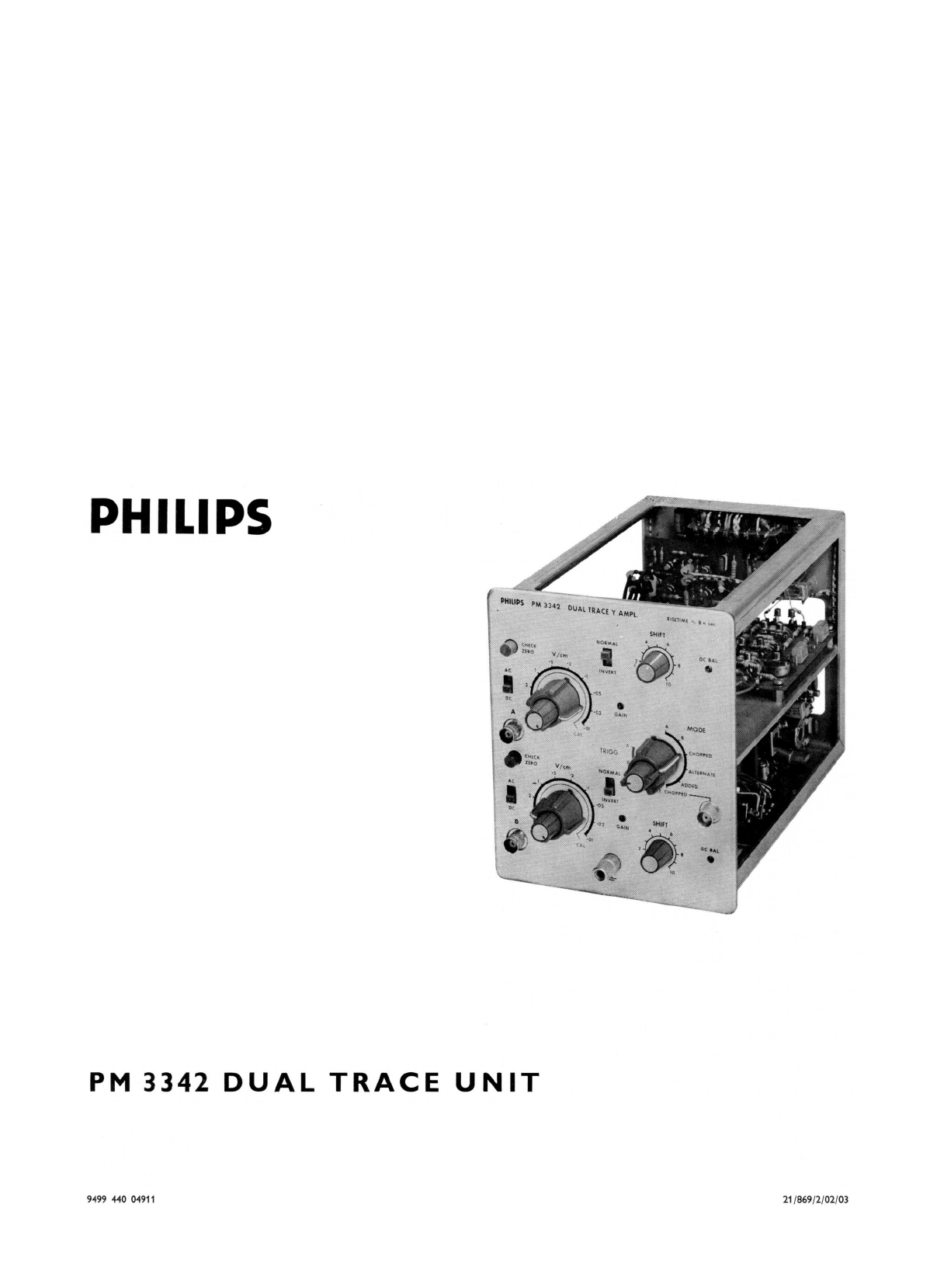
Philips PM 3342 User manual

PHILIPS
WiIUDi
PM
334
OUAI
T0.ACE
Y
AMPI
PM
3342
DUAL
TRACE
UNIT
9499
440
04911
21
869
2
02
03

3
IMPORTANT
In
correspondence
concerning
this
apparatus,
please
quote
the
type
number
and
the
serial
number
as
given
on
the
type
plate
at
the
rear
of
the
apparatus.

4
Contents
GENERAL
INFORMATION
XI.
Checking
and
adjusting
26
I.
Introduction
7
II.
Technical
data
7
A.
General
information
26
III.
Description
of
the
block
diagram
9
B.
DC
balance
26
C.
Levels
of
channels
A
and
B
27
DIRECTIONS
FOR
USE
D.
Sensitivity
of
channels
A
and
B
27
E.
AC
-DC
switch;
CHECK
ZERO
27
IV.
Installation
11
F.
Square
-wave
response
27
V.
Controls
and
their
functions
13
G.
Frequency
response
curve
29
VI.
Applications
15
H.
Defection
and
shift
29
A.
Amplitude
measurements
15
B.
Differential
measurements
15
J.
Input
attenuators
29
C.
Phase
measurements
16
K.
Blocking
of
channels
A
and
B
30
D.
Single
time
-base
16
L.
Rejection
factor
30
M.
Triggering
30
SERVICE
NOTES
N.
Cho
in
pp~
g
31
VII.
Block
diagram
17
O.
Alternate
31
VIII.
Vertical
amplifier
23
XII.
Parts
lists
32
IX.
Switching
control
-circuits
24
A.
Mechanical
33
X.
Trigger
amplifier
25
B.
Electrical
34

5
List
of
figures
Fig.
Page
1
Block
diagram
9
2
Front
view
with
indication
of
controls
and
connections
12
3
Block
diagram
(detailed)
19
4
Typical
waveforms
22
5
Display
22
6
Right-hand
view
26
7
TU-5
pulser
28
8
Left-hand
view
28
9
Measuring
probe,
directly
earthed
29
10
Input
RC
standardiser
30
ll
Amplifier,
channel
A
38
12
Amplifier,
channel
B
39
13
Dual
-trace
unit
40
14
Output
amplifier
40
15
Trigger
amplifier
41
16
Drift
compensator
41
17
Attenuator,
channel
A
44
18
Attenuator,
channel
B
48
19
Trigger
-amplifier
circuit
52
20
Dual
-trace
circuit
56
21
Y
-amplifier
circuit
61

z
GENERAL
INFORMATION
Introduction
0
The
PM
3342
is
a
dual
-trace
plug-in
unit
for
the
Y
-
channel
of
the
PM
3330.
The
unit
contains
two
identical
amplifiers
with
an
electronic
switch,
by
means
of
which
two
signals
can
be
compared
in
amplitude
and
in
phase.
Technical
data
Note:
Properties,
expressed
in
numerical
values
with
statement
of
tolerances
are
guaranteed
by
the
factory.
Numerical
values
without
tolerances
are
intended
for
information
purposes
only
and
indicate
the
properties
of
an
average
apparatus.
Input
circuit
input
input
impedance
input
maximum
permissible
d.c.
voltage
in
the
a.c.
position
Measuring
probe
type
input
attenuation
permissible
voltage
Amplifier
deflection
coefficient
Moreover,
the
sum
and
the
difference
of
two
input
signals
can
be
displayed.
Trigger
of
the
time
base
occurs
at
choice
on
one
of
the
two
input
signals
or
on
the
combined
signal.
The
amplifier
data
apply
to
channel
A
as
well
as
to
channel
B.
adjustable
AC
or
DC;
push-button
for
checking
the
zero
level
1
MS2//15pF
BNC
400
V
PM
9331
A/10
10
MS2//8
pF
1
:
10,
tol.:
3%
1,OOOVpeak
adjustable
to
10
calibrated
values:
10,20,
50
mV/cm
etc.,
up
to
10
V/cm;
tolerance:
3%
continuous
attenuator
1
:
3
(non
-calibrated)
bandwith
D.C.:
0-50
Mc/s
A.C.:
1.6
c/s
—
50
Mc/s
rise
-time
7
ns
rise
time
of
unit
by
itself:
5
ns
overshoot
<
2%
rejection
factor
>_
100
x
for
frequencies
<
1
Mc/s
in
position
D.C.
provided
that
the
amplifiers
are
adjusted
to
identical
deflection
-coefficients
maximum
common
mode
input
signal
corresponding
to
10
cm
trace
height
magnification
3
times
useful
screen
height,
symmetrical
round
the
centre
of
the
screen
for
frequencies
up
to
10
Mc/s.
The
top
of
a
signal,
which
is
magnified
at
maximum,
can
be
displayed
with
the
shift
control.

8
polarity
phase
difference
between
both
channels
Switching
possibilities
externally
chopped
voltage
required
repetition
frequency
rise
time
input
capacitance
Trigger
mode
trace
height
required
in
positions
DC,
LF
and
HF
in
position
AUT.
in
positions
TV
LINE
and
TV
FRAME
Mechanical
data
reversible
not
measurable
on
the
screen
1.
channel
A
2.
channel
B
3.
channels
A
and
B
chopped;
frequency
500
kc/s
or
20
kc/s
(internal
selection
facility)
4.
channels
A
and
B
alternately
5.
channels
A
and
B
added
6.
channels
A
and
B
externally
chopped
symmetrical
square
-wave
voltage:
minimum,
1
V
P
_p,
maximum,
20
V
p
_
p
100
kc/s
1-100
ns
70
pF
A,
B
or
A
-~
B
(in
position
"ADDED"
only)
3
mm
for
frequencies
up
to
10
Mc/s
2
cm
for
frequencies
up
to
20
Mc/s
1
cm
for
frequencies
up
to
1
Mc/s
2
cm
dimension
width
15
cm
height
17.5
cm
length
29
cm
(knobs
and
plug
included)
weight
3
kg
Accessories
1
Manual
Optional:
2
Measuring
probes
PM9331A/10

9
Description
o
f
the
block
diagram
Channels
A
and
B
each
consist
of
an
input
circuit
in
which
the
"AC
-DC"
switch
and
the
step
attenuator
are
included.,
and
an
amplifier
which
containsthe
V/cm
continuous
attenuator,
the
SHIFT
control
and
the
polarity
switch,
see
Fig.
1.
The
switching
of
these
channels
occurs
at
the
output
of
these
amplifiers,
after
which
the
combined
signal
is
applied
to
an
output
amplifier.
The
switching
circuit
consists
of
a
blocking
oscillator
A
0
CHECK
V/cm
A
C
ZEORO
~DC
20
kHz
r -
~
I...i
i
500
kHz
~T'
MODE
A
• t
--
B
•
CHOPPED
•
ALTERNATE
•
ADDED
•
EXT.-CHOPPED
O
B
O AC~
DC
r
--
b
DCBAL
Z
MOD
1
PM
3330
BLOCKING
OSCILLATOR
CATH
FOLL.
AMPLIFIER
and
a
bi-stable
multivibrator,
which
supplies
the
switching
voltage.
The
trigger
voltage
for
the
basic
oscilloscope
is
taken
from
one
of
the
channels
via
a
selector
switch.
A
trigger
amplifier
amplifies
this
voltage,
so
that
the
trigger
-
signal
and
the
Y
-input
signal
have
identical
amplitudes.
In
position
"ADDED"
of
the
"MODE"
selector,
the
trigger
signal
is
directly
taken
from
the
output
ampli-
fi
er.
NORMAL
INVERT
V'cm
CONT
I
'
~
I
SHIFT
b
GAIN
TRIGG
r
TRIGGER
AMPLIFIER
MULTIVIBRATOR
1
ELECTR.
SW
TCH
DCBAL
4
L_-
CHECK
ZERO
V
/
/CSR
\
Fig.
1.
Block
diagram
CATH
FOLL.
GAIN
V/cm
CONT
I
SHIFT
AMPLIFIER
NORMAL
INVERT
PEM
2633
I
FINAL
—~
I
Y-AMPL.
I
—
~1
I
POS.
I
ADDED]
TRIGGER
O
I
PRE-AMPL.
STAGE

11
DIRECTIONS
FOR
USE
Installation
The
PM
3342
shculd
be
plugged
into
the
left
plug-in
compartment
(Y
-UNIT)
of
basic
oscilloscope
PM
3330.
Switching
-on
is effected
with
the
mains
switch
of
the
basic
oscilloscope.
Approximately
10
minutes
after
switching
-on,
the
unit
has
reached
its
operating
temperature
and
meets
the
technical
data.
When
using
the
PM
3342,
the
switch
on
the
rear
side
of
the
basic
oscilloscope
should
be
set
to
position
"MULTI
-TRACE
CHOPPER".

12
DN~tIDS
PM
334
DUAL
iRA~
SK8
,.-=..
~
ate,,..
~
SK6
S
K
9
---~
SK
10
Fig.
2.
Front
view
with
indication
of
controls
and
connections

13
Controls
and
their
functions
(Fig.
2)
O
MODE
selector
SKS
~
~
~
i
~
~
~ ~ i i i i
~~
~~`
~~`
~
`~
~~
Trigger
mode
selector
SK6
Input
circuit
The
working
mode
of
the
unit
can
be
selected
with
the
six
-position
mode
selector.
channel
A
is
switched
in,
channel
B
is
out
of
action
channel
B
is
switched
in,
channel
A
is
out
of
action
CHOPPED
both
channels
are
switched
in.
The
volt-
ages
applied
to
sockets
A
and
B
are
elec-
tronically
switched.
The
frequency
in
which
the
channels
are
switched,
can
be
adjusted
to
20
kc/s
or
500
kc/s
with
switch
SK
11,
located
on
aprinted-wiring
board
at
the
right-hand
side
of
the
unit.
"ALTER-
channels
A
and
B
are
alternately
dis-
NATE"
played.
Switching
occurs
during
the
fl
yback
of
the
time
-base
voltage.
"ADDED"
the
voltages
at
the
output
of
both
ampli-
fiers
Aand
Bare
added.
Dependent
on
the
position
of
the
polarity
switches,
the
sum
or
the
difference
of
the
input
signals
is
applied
to
the
Y
-amplifier
of
the
basic
oscilloscope.
"EXT.
The
channels
are
switched
with
a
voltage,
CHOPPED
the
frequency
of
which
is
equal
to
that
of
BU3"
the
voltage
applied
to
socket
"EXT.
CHOPPED".
TRIGG
A
The
trigger
signal
is
equal
to
the
voltage
applied
to
socket
A.
B
The
trigger
signal
is
equal
to
the
voltage
applied
to
socket
B.
When
the
MODE
selector
is
in
position
"ADDED",
the
"TRIGG."
switch
is
out
of
action.
In
that
case
the
trigger
signal
is
taken
from
the
output
amplifier.
AC
-DC
Via
this
switch,
the
input
socket
is
con
-
switch
nected
to
the
V/cm
switch.
In
the
DC-
(SK3;
SK9)
position,
the
entire
input
signal
is
fed
to
the
V/cm
switch;
in
the
AC
-position,
the
DC
-component
is
blocked.

14
Push-button
By
depressing
this
button
the
input
circuit
CHECK
is
interrupted
and
the
amplifier
input
is
ZERO
earthed,
so
that
the
zero
level
can
be
(SKl;
SK7)
checked.
Double
With
this
double
knob
the
deflection
knob
V/cm
coefficient
of
the
amplifier
can
be
adjus-
(R3;
RS)
ted.
The
deflection
co-efficients
are
calibrated
when
the
continuous
control
is
turned
fully
clockwise
(position
CAL.).
Polarity
switch
SK2
&
SK8
SHIFT
knob
Rl
&
R7
GAIN
control
R4
&
R6
(screw
-driver
adjustment)
DC
BAL.
control
R2
&
R8
(screw
-driver
adjustment)
"NORM."
:
a
positive
-going
input
signal
causes
an
upward
deflection
on
the
screen.
"INVERT.":
a
positive
-going
input
signal
causes
a
downward
defection
on
the
screen.
With
this
knob
the
trace
can
be
shifted
in
Y
-direction.
The
working
-direction
of
this
SHIFT
knob
is
depen-
dent
o~n
the
position
of
the
polarity
switch.
The
deflection
coefficient
of
the
amplifier
can
be
checked
by
applying
the
calibration
voltage
of
the
basic
oscilloscope
to
the
input
socket.
If
the
deflection
coefficient
does
not
correspond
to
the
indicated
value,
it
can
be
corrected
by
adjusting
the
GAIN
control.
In
this
case
the
continuous
V/cm
con-
trol
should
be
turned
fully
clockwise
(CAL.).
The
DC
-balance
of
the
amplifier
can
be
adjusted
with
this
control.
For
this,
remove
the
input
signal
and
adjust
the
time
-
base
generator
to
its
fre-running
position
(TRIGG.
MODE
to
position
AUT.,
or
STAB.
fully
clockwise).
Adjust
the
DC
BAL.
in
such
way
that
the
line
on
the
screen
does
not
move
when
rotating
the
continuous
V/cm
control.

15
Applications
A.
AMPLITUDE
MEASUREMENTS
When
measuring
the
amplitude
of
a
signal,
use
is
made
of
the
calibrated
deflection
coefficients
of
the
Y
-de-
fl
ection
system
(SK4;
SK10).
Intermediate,
non
-calibrated
deflection
coefficients
can
be
obtained
by
operating
R3
and
R5.
With
the
aid
of
the
controls
of
the
basic
oscilloscope
.and
the
plug-in
unit,
make
a
triggered
display
visible.
Check
the
zero
level
by
means
of
button
CHECK
~
VLcm
ZERO
(SK1;
SK7).
(When
the
trigger
-mode
switch
is
in
the
AUT.
position,
the
time
-base
line
will
remain
visible
during
depression
of
push-button
CHECK
ZER®.
When
a
different
position
is
used,
the
time
-base
generator
should
be
adjusted
to
its
free
-running
posi-
tion
by
means
of
the
STAB.
control).
The
amplitude
of
the
total
signal
is
then
equal
to
the
product
of
deflection
coefficient
and
the
vertical
de-
fl
ection
in
cm.
Amplitude:
0.5
V/cm
x
3.4
cm
=
1.7
V.
When
only
the
AC
-voltage
should
be
measured,
the
DC
-component
can
be
removed
from
the
signal
with
the
aid
of
the
AC
-DC
switch.
If
measurements
have
been
carried
out
via
measuring
probe
PM
9331
A/10,
the
deflection
coefficient
of
the
V/cm
switch
should
be
multiplied
by
a
factor
10.
'The
accuracy
of
the
measurement
can
be
increased
by
precisely
adjusting
the
deflection
coefficient
with
the
GAIN
control
in
the
relevant
position
of
the
V/cm
knob.
For
this,
the
calibration
voltage
of
the
basic
oscillo-
scope
can
be
used.
B.
DIFFERENTIAL
MEASUREMENTS
With
these
measurements,
use
is
made
of
the
common
mode
rejection
of
the
amplifiers
in
position
ADDED.
When
the
polarity
switches
are
set
to
opposite
posi-
tions,
two
common
mode
signals
on
sockets
A
and
B
will
undergo
a
very
slight
amplification
with
respect
to
two
signals
in
anti
-phase.
The
signals
on
sockets
A
and
B
should
not
exceed
a
value
corresponding
to
a
trace
height
of
IO
cm.
This
common
mode
rejection
can
be
adjusted
to
maxi-
mum
by
adjusting
the
amplifiers
in
such
a
way
that
their
amplifications
for
the
signal
to
be
measured
are
exactly
identical.
3.4cm
0-niveau

16
Channel
A
~~
PEM
2900
Channel
B
For
this,
simultaneously
apply
one
of
the
signals
to
sockets
A
and
B.
Adjust
the
GAIN
control
in
such
a
way
that
a
minimum
trace
height
is
obtained
on
the
screen.
After
this,
the
common
mode
rejection
will
meet
the
value
mentioned
in
the
technical
data.
C.
PHASE
MEASUREMENTS
If
the
phase
difference
between
two
signals
is
to
be
measured,
the
phase
equality
of
both
amplifiers
of
the
PM
3342
is
used.
It
is
recommended
to
set
the
MODE
selector
to
posi-
tion
ALTERNATE.
With
low
repetion
frequencies
of
the
time
-base
generator,
this
working
mode
results
in
a
fl
ickering
display;
in
these
cases
the
CHOPPED
position
should
be
used.
A
high
chopper
frequency
may
lead
to
mutual
influence
of
the
two
signals;
therefore,
it
is
recommended
to
set
the
frequency
switch
to
the
20
kc/s
position.
The
signals
are
applied
to
socket
A
or
B
respectively.
Make
a
triggered
display
visible
with
the
controls
of
the
basic
oscilloscope
and
the
PM
3342.
Both
traces
should
be
adjusted
exactly
symmetrical
with
respect
to
the
centre
horizontal
graticule
line.
The
phase
difference
can
be
read
directly
in
degrees
by
adjusting
knob
TIME/cm
(step-
and
continuous
control
of
the
basic
oscilloscope)
in
such
a
way
that
one
period
of
the
signal
to
be
measured
corresponds
to
a
whole
number
of
centimetres
on
the
screen.
D.
SINGLE
TIME
-BASE
If
the
signal
to
be
measured
requires
the
use
of
the
single
-sweep
display
of
the
basic
oscilloscope,
the
MODE
switch
of
the
PM
3342
should
be
set
to
position
CHOPPED.
Selection
of
the
switching
frequency
depends
on
the
time
coefficient
of
the
X
-deflection.
V/cm,
of
both
channels:
identical
Polarity
of
channel
A:
INVERT.
Polarity
of
Chanel
B:
NORMAL
MODE
in
position:
ADDED
Generally,
the
highest
chopper
frequency
will
be
used;
for
the
lower
time
-base
speeds
however,
alsothe
lowest
chopper
frequency
can
be
selected.
Set
the
controls
in
the
TIME
BASE
A
frame
to
the
desired
positions.
When
the
time
-base
generator
is
adjusted
to
its
free
-
running
position
(STAB.
control
to
REPET),
it
will
start
immediately
after
depressing
push-button
RESET.
When
the
STAB.
control
is
in
the
trigger
position,
the
time
-base
generator
will
start
on
the
fi
rst
trigger
pulse,
after
depressing
the
RESET
button.
During
the
time
between
depression
of
the
RESET
knob
and
starting
of
the
time
-base
generator,
the
lamp
in
the
RE5ET
knob
will
light
up.
PEM
2899
1
period
=
9
cm
phase
coefficient
=
40°/cm
phase
angle
cp
=
40°/cm
x
1.6
cm
=
64°

17
SERVICE
NOTES
Block
diagram
Fig.
3
shows
that
each
channel
has
independent
control
for:
input
coupling,
attenuation,
shift,
balance
and
polarity.
The
output
of
each
channel
is
controlled
by
a
multivibrator-driven
electronic
switch,
which
feeds
the
common
amplifier.
Operation
of
this
multivibrator
in
turn
is
controlled
by
the
MODE
switch
SKS.
The
MODE
switch
can
either
hold
the
multivibrator
in
one
of
three
states
or
select
one
of
three
operating
modes
for
the
blocking
oscillator
which
drives
the
multivibra-
tor.
It
will
also
bee
seen
that
internal
trigger
signals
can
be
derived
from
one
of
three
sources:
channel
A,
channel
B
or
the
common
amplifier
output.
The
latter
is
automatically
selected
via
SKS
and
the
relay,
when
the
added
mode
is
used.
In
this
way,
triggering
on
the
desired
signal
is
possible
and
triggering
on
the
chopper
is
impossible.
Display
MODE
switch
SKS.
In
position
A
as
well
as
in
position
B,
the
multivibrator
is
held
in
the
stable
state
that
allows
the
signal
coming
from
the
selected
channel
to
pass
through
its
electronic
switch
to
the
common
amplifier.
In
the
ADDED
position,
the
multivibrator
is
held
in
such
a
state
that
both
electronic
switches
pass
their
signals
to
the
common
amplifier
where
they
are
added.
In
the
CHOPPED
position
the
blocking
oscillator
is
free
-running
either
at
1
MHz
or
at
40
kHz,
depending
on
the
position
of
SKll
(inside
the
apparatus).
Pulses
from
the
blocking
oscillator
drive
the
multivibrator,
which
supplies
anti
-phase
square
-waves
at
500
kHz
or
20
kHz
to
the
electronic
switches.
Thus:
fi
rst
the
signal
from
one
channel
will
pass
to
the
common
amplifier,

19
But
Channel
AC
®Ac
DC
V
~cm
SK3
(steps)
SKG
o-
~~
Stepped
Atten
SK9
o-
Bu3
Channel
BQ ~'
"Gate'~pulse
from
time
base
8u2
Ext.Copped
O
~
0
R8
1
M
Hz
40
kHz
Blocking
Osc
TS
502
SK
10
Stepped
Atten
dd
Check
Zero
SK1
SK7
D.C.
Bal
Cath.
Foll.
8201-6202
V/
c
m
Gain
shift
(cont)
R2
Cath.
Foll
B
301
8302
Amplifier
TS
201
-T520G
R3
i p
R1
-{
J
-
R4
-6.3V
~
SK
5
11
Bu•y
Fig.
3.
Block
diagram
(detailed)
SK
5
Amplifier
TS
301
TS
304
®
Norrcal
Invert.
SK2
moo--~
•
~~
l
l
SK8
~-o
El
Switch
T
5
206
TS209
RS
0
R7
R6
El
Switch
TS306
TS309
Channel
A
o
r
Channel
B
o
SK
6
Final
A
m
pl.
TSG01
TSG09
~~1
Bu•y
0
0 0
24V
~r
~
~
SK
5
o
Multi
vibr.
TS
503
TS
504
#z
Trigg.
Ampl.
TS
G02
IS
609
17
Bu
-y
RE
601
--~+-►16
Bu•y
—O
I
►32
Bu•y
o
f
o
~
-24V
~
SK
5
O
O
~
~---~
-z4
v
~
SK
5
0
D
SPLAY
MODE
►
Z
-Mod.
A
9
Bu
-y
B
o
0
Chopped
SK
5
Alternate
a
Addedo
p
Extchopped
o
b
24V
0
p
SK
5
0
PEM
2897

22
1
2
3
4
5
6
7
0
1
2
3
4
5
6
7
8
1
2
3
4
5
6
7
8
1
2
3
4
5
6
7
0
1
2
3
4
5
6
7
8
1
Input
channel
A
Input
channel
B
Time
-base
sweeps
I
2
3
L
Output
Vertical
amplifier
Fig.
4.
Typical
waveforms
II
II
Iff
1Y
2
3
L
5
TY
then
that
from
the
other.
In
this
way,
the
spot
will
fol-
low
apart
of
each
signal
in
turn
as
shown
in
Fig.
4
and
as
it
will
not
be
the
same
part
each
sweep,
the
persis-
tance
of
vision
(and
sometimes
that
of
the
CRT)
will
create
the
illusion
of
two
complete
waveforms
on
the
screen,
as
shown
in
Fig.
5.
To
prevent
hazing
as
the
spot
moves
from
one
trace
to
the
other,
blanking
pulses,
derived
from
the
blocking
oscillator,
are
fed
to
the
CRT
via
9
BU
-Y.
II
I
IY
I
II
II
I
3
L
5
6
Fig.
S.
Display
~~
3
L
5
6
7
_~
I
II
~-
5
6
7
0
I
_~
PEM
2898
In
the
EXT.
CHOPPED
position,
operation
is
the
same
as
for
CHOPPED,
except
that
now
the
blocking
oscillator
will
not
be
free
-running
but
has
to
be
trig-
gered,
via
BU2,
by
an
external
signal.
In
the
ALTERNATE
position,
the
blocking
oscillator
is
triggered
during
the
fl
y
-back
of
the
time
-base.
Thus
the
spot
traces
out
fi
rst
one
signal
and
then
the
other.

23
Vertical
am~li
Fier
1.
Pre
-amplifier
channel
A
(Fig.
21)
The
incoming
signal
is
fed
directly
or
via
a
capacitor
depending
on
the
position
of
switch
SK3
(AC
-DC),
to
a
10
-step
attenuator,
which
reduces
the
signal
amplitu-
de
by
afactor
1,
2,
5,
10
etc.
up
to
1000,
as
selected
with
switch
SK4
(V/cm).
Cathode
-follower
B201
provides
an
impedance
trans-
formation
to
drive
the
following
transistor
amplifier.
As
the
cathode
-follower
is
subject
to
some
DC
-drift,
a
second
cathode
follower
B202
is
symmetrically
con
netted
to
it
to
minimise
drift.
Furthermore,
provision
is
made
to
balance
the
amplifier
by
varying
the
grid
potential
of
B202
at
R321
"COARSE
DC
-BALANCE"
and
R2
"DC-BAL".
When
properly
adjusted,
no
signal
will
be
present
across
R3
(CONTINUOUS
CONTROL)
if
the
grid
circuit
of
B201
is
connected
to
earth
with
switch
SK1
("CHECK
ZERO").
Clamping
diodes
GR202
and
GR203
prevent
the
tran-
sistor
amplifier (TS201-TS202)
driving
signal
from
becoming
intolerably
high
in
either
the
positive
or
the
negative
direction.
Protecting
diode
GR201,
which
is
normally
forward
biased,
p~
events
the
maximum
(negative)
grid
-to
-cathode
voltage
from
being
exceeded,
because
if
such
a
signal
is
present,
protecting
diode
GR201
will
be
reversely
biased.
The
cathode
voltage
will
then
be
determined
by
the
—150
Volts
supply
and
the
voltage
-drop
across
R206
due
to
the
cathode
cur-
rent.
To
complete
the
temperature
-compensation,
the
cathode
circuit
of
B202
is
likewise
provided
with
diode
GR206
of
the
same
type.
Diode
GR204
prevents
high
voltages
from
being
applied
to
TS202.
The
second
stage
is
formed
by
emitter
-followers
TS201
and
TS202.
They
offer
a
low
impedance
signal
source
for
the
next
stage
and
for
the
trigger
-amplifier,
which
receives
its
signals
via
R232
and
R237.
From
conti-
nuous
control
R3,
the
signal
is
routed
to
the
third
stage,
TS203-TS204.
This
stage
can
be
regarded
as
an
asymmetrically
driven
long
tailed
-pair
amplifier.
The
output
of
this
stage
consists
of
two
equal,
but
opposite,
signals.
GAIN
control
R4
influences
the
negative
feedback
and
consequently
the
amplification
factor.
R235
and
C211
provide
a
correction
to
obtain
optimum
step
-response.
Shift
controls
Y
-SHIFT
(R1
-R1')
and
the
polarity
switch
SK2
are
inserted
between
the
third
and
fourth
stage.
The
connections
from
the
third
stage
to
SK2
and
from
SK2
to
the
fourth
stage
are
effected
by
means
of
a
300
Ohm
ribbon
line,
which
is
terminated
by
R249
and
the
series
-connection
of
R254
-R256.
The
power
is
supplied
at
the
junction
of
R254
-R256.
In
this
way,
the
total
dynamic
resistance
at
the
collectors
of
TS203
and
TS204
amounts
to
75
Ohms.
The
fourth
stage
consists
of
two
cascode
amplifiers
(TS206-TS208
and
TS207-TS209)
which
are
push-pull
connected.
Transistors
TS206
and
TS207
act
as
current
sources
to
the
low
-ohmic
inputs
of
TS208
and
TS209
respectively.
Thus
hardly
any
signal
voltage
will
be
present
at
the
emmitters
of
TS208
and
TS209,
so
it
is
possible
to
carry
out
the
electronic
switching
at
this
point.
If
the
voltage
at
R508
becomes
more
positive
than
the
emitter
voltage,
switching
diodes
GR209
and
GR211
are
blocked,
thus
allowing
normal
operation
of
the
cascode-amplifiers.
If
the
voltage
at
R508
is
decreased
below
the
potential
at
the
bases
of
TS208
and
TS209,
the
transistors
are
fully
blocked
and
diodes
GR208
and
GR212
likewise.
So
no
signals
will
pass
and
channel
A
is
cut
off.
In
the
emitter
circuit
of
TS206
and
TS207,
R263
and
C217
provide
low
frequency
compensation;
C218
improves
the
step
-function
response.
2.
Pre
-amplifier
channel
B
(Fig.
21)
This
pre
-amplifier
is
identical
to
that
of
channel
A.
The
switching
voltage
of
channel
B
however,
is
counter
-
phased.
Thus
the
diodes
GR309-GR311
are
conductive
when
GR209-GR211
are
blocked
and
vice
versa
.As
a
result,
the
signal
of
channel
A
is
displayed
when
channel
B
is
blocked
and
vice
versa.
3.
Output
amplifier
(Fig.
21)
The
driving
signals
of
the
output
amplifier
are
devel-
oped
across
R402
and
8406.
Emitter
-followers
TS401-
TS402
offer
these
signals
with
a
low
source
impedance
to
cascode-amplifiers
TS403-TS406
and
TS404-TS407
The
amplified
signals
are
fi
nally
routed
to
the
output
stage
consisting
of
emitter
followers
TS408-TS409
which
make
them
available
to
the
vertical
amplifier
of
the
basic
oscilloscope
via
terminals
1
and
17
of
BU
-Y.
When
the
MODE
-switch
SKS
is
in
position
ADDED,
diodes
GR209-GR211-GR309-GR311
are
blocked
simultaneously
so
that
both
channels
are
switched
in
and
a
combined
signal
is
applied
to
the
output
ampli-
fi
er.
To
maintain
the
same
voltage
-level
at
R404,
R401
is
connected
in
parallel.
The
two
cascode-amplifiers
are
connected
in
push-pull
arrangement
with
a
high
common
resistance
at
the
emitter
side
of
TS403-TS404
thus
forming
one
differen-
tial
amplifier.
C422,
C401
and
R413
improve
the
step-
functionresponse.

24
Switching
control
circuits
1.
Blocking
oscillator
(Fig.
20)
1f
SKS
is
in
the
CHOPPED
position,
switch
SKS
IA
is
open,
so
that
the
potential
at
the
base
of
TS502
is
de-
termined,
by
voltage
-divider
R
504-506.
It
is
adjusted
so
that
the
blocking
oscillator
becomse
astable,
oper-
ating
at
a
repetition
rate
of
40
kHz
or
1
MHz
depending
on
the
position
of
SK11).
In
all
other
positions
of
SKS
,switch
SKS
lA
is
closed,
thus
setting
the
base
to
approximately
emitter
-potential.
TS502
is
almost
cut-off
but
it
will
operate
when
a
nega-
tive
pulse
arrives
at
the
base
from
terminal
4
of
S2
(transformer
T501).
If
SKS
is
in
the
ALTERNATE
position,
C500
and
R511
differentiate
anegative-going
pulse,
which
arrives
at
terminal
11
BU
-Y
and
which
has
the
same
duration
as
the
GATE
pulse
of
the
basic
oscilloscope.
The
posi-
tive
-going
spike
resulting
from
the
trailing
edge,
is
passed
by
diode
GR507
to
emitter
-follower
TS501,
which
injects
it
into
winding
SS
of
transformer
T501.
The
inverted
pulse
is
applied
to
the
base
of
TS502,
which
triggers
the
blocking
oscillator
to
deliver
one
pulse,
after
which
the
oscillator
returns
to
its
quiescent
state.
If
SKS
is
in
the
EXT.
CHOPPED
position,
the
signal
entering
at
BU2
is
differentiated
by
C500
and
R511
and
triggers
the
blocking
oscillator
as
mentioned
under
ALTERNATE.
Every
time
the
blocking
oscillator
operates,
a
pulse
appears
at
winding
S1
of
transformer
T501.
It
is
routed
to
terminal
9BU-Y
to
momentarily
blank
the
display
on
the
sereen.
To
ensure
that
the
blanking
pulses
reach
the
CRT
at
the
moment
that
the
switching
pulse
(delayed
by
the
vertical
amplifier)
reaches
the
Y
-deflection
plates,
a
120
nanosecond
delay
-line
is
fi
tted
in
the
main
frame.
Resistor
R503
(470
S2)
ter-
minates
this
delay
line
to
avoid
reflections.
2.
Multivibrator
(Fig.
20)
The
bi-stable
multivibrator
TS503-TS504
is
locked
in
postition:
TS503
cut-off.
TS504
conductive,
when
MODE
selector
SKS
is
in
position
A.
As
a
result,
the
electronic
switch
of
channel
A
is
closed
and
that
of
channel
B
is
open.
When
SKS
is
in
position
B,
TS504
is
blocked
and
the
signal
of
channel
B
is
displayed.
When
SKS
is
in
the
ADDED
position,
both
transistors
are
blocked
and
both
electrcnic
switches
are
therefore
closed.
When
SKS
is
in
the
CHOPPED,
ALTER-
NATE
ar
EXT.
CHOPPED
positions,
the
bi-stable
multivibrator
switches
at
half
the
rate
of
the
blocking
oscillator.
It
may
be
observed
that
switching
diodes
GR501
and
GR502
are
conductive
when
their
appertaining
tran-
sistors
are
conductive.
They
then
offer
a
low
ohmic
path
to
an
incoming
negative
switching
pulse.
The
transistor
will
be
blocked
and
also
the
diode
which
will
then
turn
into
ahigh-ohmic
impedance.

25
Trigger
amplifier
O
The
trigger
amplifier
(Fig.
19)
consists
of
four
push-pull
stages
which
are
directly
coupled
to
each
other.
The
fi
rst
three
stages
are
long-tailed
pair
amplifiers:
the
fourth
stage
is
connected
as
an
emitter
-follower
output
—stage.
The
balance
of
the
amplifier
is
adjusted
at
the
fi
rst
stage
by
R605;
the
quiescent
DC
-level
of
the
output
is
ad-
justed
by
changing
the
value
of
R623.
The
output
of
the
trigger
amplifier
is
connected
to
the
trigger
amplifier
of
the
main
frame
via
contacts
of
relay
RE601.
When
MODE
selector
SKS
is
in
the
ADDED
position,
the
relay
is
energised
and
the
output
of
the
trigger
amplifier
is
disconnected.
The
main
frame
trigger
am-
plifier
is
then
connected
to
the
output
of
the
vertical
amplifier.

26
Checking
and
adjusting
A.
GENERAL
INFORMATION
The
tolerances
mentioned
are
factory
tolerances;
they
apply
when
the
apparatus
is
readjusted
completely.
They
may
differ
from
the
data
given
in
II.
A
summary
of
the
adjusting
elements,
their
nomencla-
ture
and
location
has
been
given
in
V.
With
the
aid
of
these
data,
it
is
possible
to
carry
out
all
the
adjustments
of
the
dual
trace
unit
PM
3342
and
to
check
the
proper
working
of
the
plug-in
unit.
For
this,
the
unit
should
be
inserted
into
the
Y
-plug-in
compartment
of
a
correctly
adjusted
basic
oscilloscope
PM
3330.
Some
of
the
adjusting
elements
are
on
the
right-hand
side
of
the
unit
and
are
not
directly
accessible.
When
these
elements
must
be
adjusted,
the
unit
should
be
connected
to
the
basic
oscilloscope
via
the
rigid
exten-
sion
plug
(code
number
4822
263
70009).
For
a
complete
adjustment
of
the
instrument
the
se-
quence
as
described
in
this
chapter
is
to
be
preferred.
R
313
Fig.
6.
Right-hand
view
B.
D.C.
BALANCE
This
adjustment
should
be
carried
out
when
the
unit
has
obtained
its
operating
temperature,
i.e.
approxi-
mately
15
minutes
after
switching
-on.
Set
the
knobs
of
the
basic
oscilloscope
to
the
following
positions:
"TRIGG.
MODE":
"AUT."
"TRIGG.
SOURCE":"[NT."
"TIME/cm":
"2
msec./cm"
"X
-DEFLECTION":
"TIME
BASE
A"
1.
Channel
A
R213
(Fig.
6)
Set
"MODE"
(SKS)
to
"A"
and
turn
"D.C.
BAL."
(R2)
to
its
mid
-position.
During
this
adjustment,
keep
the
time
-base
line
on
the
screen
with
"SHIFT"
(R1).
—
Adjust
the
coarse
control
"D.C.
BAL."
(R213)
so,
that
the
time
-base
line
hardly
moves
when
"V/cm"
(R3)
is
turned
fully
clockwise
or
anti
-clockwise.
—
With
the
fi
ne
control
"D.C.
BAL."
(R2),
adjust
for
a
stationary
display.
I
R
213
TS
608
TS
609
TS
602
TS
603
15
Table of contents
Other Philips Amplifier manuals

Philips
Philips TDA8925 User manual

Philips
Philips CMP400 User manual

Philips
Philips BGY148A User manual

Philips
Philips CMP200 User manual

Philips
Philips TDA2615 User manual

Philips
Philips FA741 User manual

Philips
Philips BGY1916 User manual

Philips
Philips TFA9843AJ User manual

Philips
Philips UA747C Owner's manual

Philips
Philips 32PW9556-05R User manual

Philips
Philips TDA7057AQ User manual

Philips
Philips TDA2616 User manual

Philips
Philips BGY86 User manual

Philips
Philips CMP200/93 User manual

Philips
Philips BGY583 User manual

Philips
Philips TDA6111Q User manual

Philips
Philips BGY885B User manual

Philips
Philips FA 950 User manual

Philips
Philips BGY2016 User manual

Philips
Philips 22AH396 User manual