Philips CU1216 Series User manual

BU RF Solutions
- 1-
CU1216/TU1216 Family
Evaluation Board
Copyright © Philips Electronics Singapore Business Unit RF-Solutions 2004

BU RF Solutions
- 2-
Table of Contents Page
Introduction 4
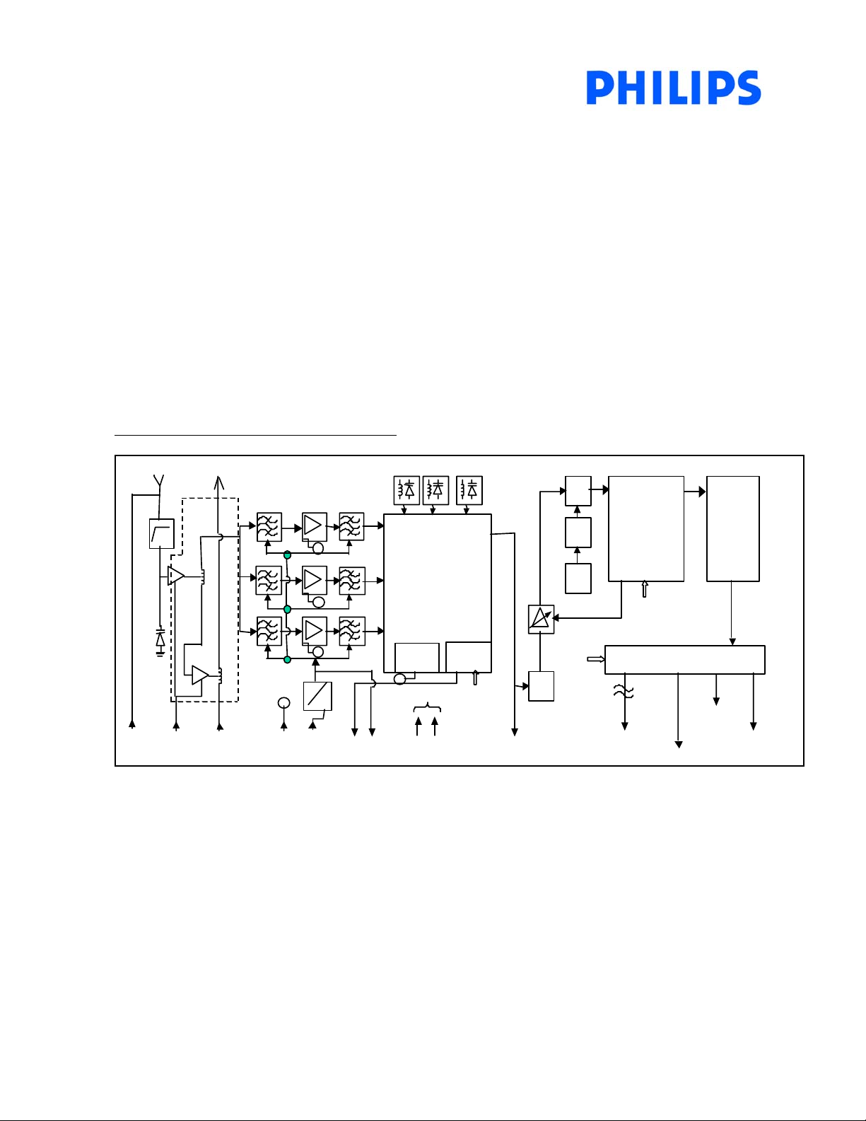
1. General Block Diagram and Descriptions 4
2.PinningConfigurations 6
3. Quick Startup Guide for User 7
4. An overview of the Evaluation Board 8
4.1 Board Settings 10
4.1.2 Board Power Supplies 10
4.1.3 Connectors 10
4.1.4 Jumper Configurations 11
4.1.5 Hard Reset 11
5. Channel Decoder Software Guide And Installation 12
5.1 Software Installation 12
5.2 Channel Decoder TDA10021 12
5.2.1 TDA10021 – Control Software Windows 12
5.2.2 TDA10021 - A Quick Guide to software Usage 16
5.3 Channel Decoder TDA10046 16
5.3.1 TDA10046 -- Control Software Windows 16
5.3.2 TDA10046 – A Quick Guide to software Usage 20
5.4 Trouble Shooting 21
List of Figures
Figure 1.1 CU1216 General Block Diagram 4
Figure 1.2 TU1216 General Block Diagram 5
Figure 4.1 Evaluation Board Layout 8
Figure 4.2 Physical Evaluation Board 9
Figure 5.1 TDA10021 Main User Interface Window 13
Figure 5.2 TDA10021 Board Configuration Window 14
Figure 5.3 TDA10021 Registers under lock condition 15
Figure 5.4 TDA10046 Main User Interface Window – Download DSP code 17
Figure 5.5 TDA10046 Main User Interface Window 17
Figure 5.6 TDA10046 Board Configuration Window 19
Figure 5.7 TDA10046 Registers 19
List of Tables
Table 2.1 Pinning Configurations 6
Table 5.1 Descriptions for the TDA10021 main user interface window 13
Table 5.2 Descriptions for the TDA10021 board configuration window 15
Table 5.3 Descriptions for the TDA10046 main user interface window 18
Table 5.4 Descriptions for the TDA10046 board configuration window 19
Appendix A : Evaluation Board Schematic Diagram 22

BU RF Solutions
- 3-
Document Release History
Date Revision Remarks Editor
08 Oct 2003 1_0 First release Lim Kui Yong / Elicia Tiah
14 Jan 2004 1_1 1) Block Diagram and pinning update
2) TDA10021 Software Version update (ver 2.8)
Elicia Tiah

BU RF Solutions
- 4-
Introduction
This application note describes the use of our common CU/TU1216 NIM (Network Interface Module) evaluation
board that include both the hardware and software requirements.
A general block diagram and description will be provided for better product understanding.
1. General Block Diagram and Descriptions
In general, the CU1216 and TU1216 family is a single conversion full band Network Interface Module (NIM) with
a built- in PLL tuner and a Single Chip DVB-C and DVB-T Channel Decoder respectively.
For details of the model types, please refer to the respective datasheets. This test board can support all models as
mentioned.
Figure 1.1 : CU1216 general block diagram
Oscillators
I2
5V
A
A
A
A
I2
Detector
A
RFAGC
xtal
PLL
A
DC
I2
Core
I2CBUS
IF AGC
PLL
CBUS
IF
MOPLL I
C
SDASCL
CBUS
A
GC
MPEG (D ....D7/SER)
MP EG_T S_CLK
MP EG_D ATA_ VAL
MPEG_ PKT_SYNC
SAW
Output Formatter
CBUS
Demodulation Error
Recovery
A
S
33V
+5V
A
GC Vt
+5V(LT)
RFinput
RFMod in
RFout
A
nt_5 V
Active
Loopthrough
The module consists of the following key features :
1. Loopthrough / RF Modulator input function – Passive loopthrough (LS), Active loopthrough (L) and Active
loopthrough/RF Mod input (LM) versions are available.
2. Tuner – high performance single conversion tuner that covers a frequency range from 51Mhz to 858Mhz.
33V tuning supply is derived from the single 5V supply by means of a DC/DC converter.
3. IF – Provides wideband IF output 36.15Mhz for analog reception. The narrowband IF output after SAW
filtering is being amplified further by a variable IF amplifier. This is controlled by the digital demodulator in
order to maintain a 2Vp-p differential amplified IF output to the DVB-C Receiver.
4. Digital Demodulator -- TDA10021 is used which can support up to 256QAM. The output can be either a
parallel or a serial MPEG-2 transport stream.

BU RF Solutions
- 5-
Figure 1.2 : TU1216 general block diagram
1.
2.
3.
4.
5.
6.
7.
8.
9.
10.
11.
12.
13.
14.
15.
16.
17.
18.
19.
20.
The module consists of the following key features :
1. Loopthrough / RF Modulator input function –Active loopthrough/RF Mod input (LM)
2. Tuner – high performance single conversion tuner that covers a frequency range from 51Mhz to 858Mhz.
33V tuning supply is derived from the single 5V supply by means of a DC/DC converter.
3. IF – Provides wideband IF output 36.15Mhz for analog reception. The narrowband IF output after SAW
filtering is being amplified further by a variable IF amplifier. This is controlled by the digital demodulator in
order to maintain a 2Vp-p differential amplified IF output to the DVB-T Receiver.
4. Digital Demodulator -- TDA10046 is used which can support up to 2K and 8K COFDM Modes. The
output can be either a parallel or a serial MPEG-2 transport stream.
R
F-inpu
t
R
F
/
m
od.
outpu
t
+5Vspli
t
t
e
r
supply
v
oltage
(op
t
ional)
OP
T
ION:
A
n
t
enna po
w
e
r
O
P
T
ION
:
M
o
dula
t
o
r
inpu
t
(4)(2) (1)
S
A
W
high-
band
m
id
-band
lo
w
-band
o
s
c
.
o
s
c
.
os
c
.
33
V
V
5
V
t
une
hi
gh
mi
d
lo
w
A
GC +5
V
t
une
r
suppl
y
vol
t
age
.
M
O
P
L
L
P
L
L
IC-BUS
2
A
GC
loop
A
G
C
loop
4M
Hz
c
r
y
s
t
al
r
e
f
e
r
e
n
c
e
IF- ou
t
pu
t
(b
r
oadband)
+1.8
V
supply+3.3V
suppl
y
MPEG
_
TS
(D0...D7
/
se
r
ial) MPEG
_
TS
_
CL
K
Rese
t
MPEG
_
P
K
T
_
S
Y
N
MPEG
_
D
A
T
A
_
V
A
L
(5) (6
)(24
/
25) (28)(27)
(13)(11) (12) (15...22) (23)
(26)
IC-BUS
IC
-
BUS
2
2
L
o
o
p
t
h
r
o
u
g
h
o
p
t
i
o
n
2
k
/
8
k
C
O
F
D
M
c
h
a
n
n
e
l
d
e
c
o
d
e
r
.
.
.

BU RF Solutions
- 6-
2. Pinning Configurations
Both CU and TU have common pinning configurations. Refer to Table 2.1.
PIN SYMBOL DESCRIPTION
1 RF Mod_in RF Modulator input (depends on versions)
2 Ant_5V Antenna 5V [Do not connect if active antenna is not used.]
3 N.C Not connected
4 5V (LT) Loop Through Supply Voltage +5V (depends on version)
5 AGC Automatic Gain Control (external) +4V
[Do not connect for normal usage with Wideband AGC]
6 5V Tuner Supply Voltage +5V
7 AS NIM Address Select
8 Vt Tuner Tuning Voltage
[For monitoring purpose only, do not connect to power supply]
9 N.C Not connected
10 GND Ground
11 1.8V Supply +1.8V
12 3.3V Supply +3.3V
13 IF Intermediate Frequency (unfiltered)
14 GND Ground
15 MPEG D0/SER Parallel MPEG Transport Output Data Bit 0/Serial Output
16 MPEG D1 Parallel MPEG Transport Output Data Bit 1
17 MPEG D2 Parallel MPEG Transport Output Data Bit 2
18 MPEG D3 Parallel MPEG Transport Output Data Bit 3
19 MPEG D4 Parallel MPEG Transport Output Data Bit 4
20 MPEG D5 Parallel MPEG Transport Output Data Bit 5
21 MPEG D6 Parallel MPEG Transport Output Data Bit 6
22 MPEG D7 Parallel MPEG Transport Output Data Bit 7
23 MPEG_TS_CLK MPEG Transport Stream Clock
24 SDA I
2C-Bus Serial Data
25 SCL I
2C-Bus Serial Clock
26 RST Reset
27 MPEG_DATA_VAL MPEG Data Valid
28 MPEG_PKT_SYNC MPEG Packet Sync
29 MPEG_ERR MPEG error out
30 N.C Not connected
31 N.C Not connected
32 N.C Not connected
M1,M2,
M3,M4
GND Mounting Tags (Ground)

BU RF Solutions
- 7-
3. Quick Startup Guide for the user.
A quick guide is as followed. Further information and instructions for hardware and software requirements are
given in the next sections.
1) Apply +5V power supply at connector 1000.
2) Connect parallel port from IIC controller (PC), which generates the IIC protocol connector 1040 (IIC Input
Connector).
3) Set Tuner Address Select/ AS to C0 by putting a jumper at pin 3 & 4 of connector 1034.
4) Load DUT at socket 1030.
5) For CU1216, load TDA10021 software and follow the software instruction guide as in section 5 OR
6) For TU1216, load TDA10046 software and follow the software instruction guide as in section 5.
7) Connect the QAM/COFDM input signal at RFin connector of the DUT. Check min supply current.
CU1216LM = 380mA
CU1216LS = 340mA
CU1216A = 336mA
TU1216L = 380mA
If not, reset board at connector 1038 with a jumper.
8) MPEG2 TS output available at connector 1020 for further MPEG2 decoding.

BU RF Solutions
- 8-
4. An Overview of the Evaluation Board
The evaluation board can be classified to few different sections. Refer to Diagram 4.1 /4.2.
A. +5.0Volts power supply, 3.3Volts and 1.8Volts supplies via stabilizers for digital part.
B. On-board IIC Interface.
C. LVDS interface for output MPEG2 Transport Stream.
D. Common socket to install CU1216 or TU1216 product.
E. CU1216 DVB_C & TU1216 DVB_T receiver.
The dimension of this board is approximately 150mm by 110mm.
Figure 4.1 : Evaluation Board layout
(C ) LVDS interface for
MPEG2 Transport Stream O/p
IIC Input
Connector
(
D
)
Common Socket for DUT
IF O/p
+1.8V o
p
tion
(B) On board IIC Buffer
+2.5V option
+5V Ant Power u
p
o
p
tion +4V Ext AGC
PLL Address
Select
1 3
2 4 1 3
2 4
+3.3V Supply
Power reset
(E) CU1216 DVB-C /
TU1216 DVB-T
2 1

BU RF Solutions
- 9-
Figure 4.2. Physical Evaluation Board

BU RF Solutions
- 10 -
4.1. Board Settings.
4.1.1 Board Power Supplies
+5.0 Volts
A single 5Volts supply is needed via connector 1000. The 5 Volts is further regulated to different voltages
required by the CU1216 and TU1216 products.
- +3.3V supply via stabilizer 7000.
- +1.8V / 2.5V supply via stabilizer 7001.
- +4V external AGC supply via potentiometer 3034.
Tuning supply voltage
The tuning supply voltage is generated by the DUT. No external tuning voltage needed.
4.1.2. Connectors
1000 :
5Volts supply with pin 1 (+5V) and pin 2 (Gnd)
1033 :
Power Splitter output (BNC)
1037
: IF Output (BNC)
1030 :
DUT socket
1040
: IIC communication (D25 male) with the following pinnings :
Pin Description Pin Description
1 RESET SDD 14
2 15
3 16
4 17 CLK
5 18
6 19
7 20
8 21
9 SDA 22
10 GND 23
11 ACK 24
12 25 GND
13 GND
1020 :
Transport Stream Output with the following pinning :
Pin Description Pin Description
1 PD0CLK+ 14 PD0CLK-
2 GND 15 GND
3 PDO7+ 16 PDO7-
4 PDO6+ 17 PDO6-
5 PDO5+ 18 PDO5-
6 PDO4+ 19 PDO4-
7 PDO3+ 20 PDO3-
8 PDO2+ 21 PDO2-
9 PDO1+ 22 PDO1-
10 PDO0+ 23 PDO0-
11 PDOVAL+ 24 PDOVAL-
12 PDOSYNC+ 25 PDOSYNC-
13 GND

BU RF Solutions
- 11 -
4.1.3. Jumper Configurations
1001 :
+2.5Volts option
1002 :
+1.8Volts option
1031 :
+5.0Volts Antenna Power Up option
1034
: PLL synthesizer Address Selection option:
AS1 = C6 (pin 1 & 3)
AS1 = C0 (pin 2 & 4)
1035 :
PLL synthesizer Address Selection option /AS0. (not application for CU/TU1216)
1039 :
+1.2Volts supply option (not application for CU/TU1216)
1036 :
+4.0Volts External AGC supply option
4.1.4. Hard Reset
Connect Jumper 1038 to do a hard reset on the DUT.

BU RF Solutions
- 12 -
5. Channel Decoder Software Guide and Installation
This section provides some instructions for the channel decoder software installation and a quick guide to
use it.
CU1216 family uses the TDA10021 channel decoder intended for the reception of DVB_C compliant
MPEG2 signals, transmitted via cable networks.
TU1216 family uses the TDA10046 channel decoder intended for the reception of 2K/8K DVB_T
Compliant MPEG2 signals, transmitted via OFDM modulated techniques.
5.1 Software Installation
To install the software, copy all delivered files under a specific directory. It is advisable to use PC controller
with at least Pentium I processes. If the OS used in the PC controller is Window 98 or Window ME, no
driver is needed. For Windows NT, install the proper driver (read in Readme file)
To activate the program, double click on the registration file (.REG) followed by the executable file
(.EXE).
5.2 Channel Decoder TDA10021
This section is meant for CU1216 family only. For the details, please refer to TDA10021datasheet and
application notes.
5.2.1 TDA10021 - Control Software Windows
Examples of the software control windows are illustrated as followed.

BU RF Solutions
- 13 -
FIGURE 5.1 : TDA10021 MAIN USER INTERFACE WINDOW
Table 5.1 Descriptions for the TDA10021 main user interface window
Channel Configuration
RF in [MHz] Set the RF input signal frequency in MHz
SR [Mbaud] Set the symbol rate for the channel decoder in Msps
Modulation Set the QAM format (4, 16, 32, 64, 128 or 256QAM)
Spectral inversion Automatic search for spectral inversion or force the spectal inversion
Program Fron-End Run the algorithms to lock the complete system
Channel Status
BER BER indication after the demodulation (RS decoder input)
RF AGC / IF AGC Value between 0 and 255 indicating the tuner AGC level. 0 = to much power/ 255
= not enough power
MSE Mean square error indicating the signal quality (low MSE means good signal quality)
AFC=xxKHz Indication of the corrected frequency drift in KHz
Activate Register Mode
Tuner Setup Window
Scattering Diagram
LEDs indicators
BER graph
Activate scanning mode
IIC Control Window
Demodulator Setup Window
Channel
Settings
Program tuner and TDA10021
BER value
Tuner AGC and IF AGC indicator

BU RF Solutions
- 14 -
LEDs indicators
• Tuner Lock
Indicator will turn green when tuner is successfully locked to a wanted frequency.
• Carrier Lock
Indicator will turn green when channel decoder has detected a QAM signal.
• Frame Synchronization
Indicator will turn green when the FEC has established synchronization with the MPEG structure of the source
packets.
• Frontend Lock
Indicator will turn green when IIC Communication has been established with the channel decoder.
• Uncorrected Blocks
Indicator will turn green when there are no uncorrected data blocks received by decoder.
FIGURE 5.2 : TDA10021 BOARD CONFIGURATION WINDOW
Set to CUSTOM
MPEG TS
Configuration
Sampling
Clock Control
Tuner
Configuration
Tuner and IF
settings
(TOP control
for tuner)
TDA10021
Configuration;
Equalizer type

BU RF Solutions
- 15 -
Table 5.2 Descriptions of the TDA10021 board configuration window
Tuner configuration
Tuner type Select the type of tuner. If another tuner is used, select none.
IF frequency Enter the IF center frequency delivered by the tuner (36.125 or 43.75Mhz).
Enable reading Enable/disable to read the tuner PLL status. When enabled, the “?” mark in the main
window disappears and indicates if the PLL is locked or not. Must be disabled in normal
operation to avoid some parasitics phenomenon on the tuner.
Spectral inversion Enter a possible spectral inversion in the tuner if it is known
Demodulator
BER counter depth Defines over many symbols the BER is measured. For BER values, the value must be set
to 108to get a reliable and stable value.
Equalizer Set the type of Equalizer (DFE or Linear Transversal) or disable the equalizer
MPEG TS output1 Configure the MPEG TS output pins (parallel mode or serial mode)
MPEG TS output2 Configure the MPEG TS output pins serial mode only delivered on the JTAG pins when
ENSERI pin is set to ‘1’
PLL (Set to CUSTOM under Board to enter wanted frequency and PLL factors)
Crystal frequency Specifies the Xtal frequency connected to the TDA10021
PLL factors (M, N, P) Set the different divider ratios of the PLL
FIGURE 5.3 : TDA10021 registers under lock condition
MPEG TS status :
Disable : CONTROL register (index 2c) = 0f
Enable : CONTROL register (index 2c) = 0d (for further decoding purpose)

BU RF Solutions
- 16 -
5.2.2 TDA10021 – A Quick Guide to Software Usage
After the tuner is powered up for proper initialisation, the program can be launched.
(Hint : Tuner OK indicator should be on to indicate 5V supply and IIC communication have been detected)
Test procedure for CU1216 family :
1) Input the followings in the Main User Interface menu (refer to Figure 5.1) :
- Wanted RF frequency
- Symbol rate, SR, e.g. 6.95M Baud
- Modulation, e.g. 64QAM, 256QAM
2) Pull down the View icon, select Board Configuration, which allow the user to set the TDA10021 Board
configuration. Necessary inputs are as followed (refer to Figure 5.2) :
- Under Board, select Custom
- Under PLL, enter crystal frequency = 28920000Hz and PLL factor = M : 8 N : 1 P : 4
Return back to Main User Interface menu; press successively the « Program Front-end » button. The
system should lock immediately.
5.3 Channel Decoder TDA10046
This section is meant for TU1216 family only. For the details, please refer to TDA10046datasheet and
application notes.
5.3.1 TDA10046 - Control Software Windows
Examples of the software control windows are illustrated as followed.

BU RF Solutions
- 17 -
FIGURE 5.4 : TDA10046 MAIN USER INTERFACE WINDOW – Download DSP code
FIGURE 5.5 : TDA10046 MAIN USER INTERFACE WINDOW
Load in DSP code
DSP code icon
Activate Register Mode
LEDs indicators
Channel
Settings
Program tuner and TDA10046
BER value
Tuner AGC and IF AGC indicator
IIC Control Window
Tuner Setup Window
Scattering Diagram
BER graph
Demodulator Setup Window
Activate scanning mode

BU RF Solutions
- 18 -
Table 5.3 Descriptionsfor the TDA10046 main user interface window
Channel Configuration
RF in [MHz] Set the RF input signal frequency in MHz
Bandwidth [MHz] Set the BW for the channel decoder in MHz
Modulation Set the modulation format (QPSK, 16QAM, 64QAM)
Spectral inversion Automatic search for spectral inversion or force the spectal inversion
Guard Interval Set guard Interval (Auto, 1/32, 1/16, 1/8, 1/4)
FFT size Set FFT size (Auto, 2K, 8K)
Channel Set Channel (HP, LP)
VR HP/LP Set code rate (1/2, 2/3, ¾, 5/6, 7/8)
Program Fron-End Run the algorithms to lock the complete system
Channel Status
AFC=xxKHz Indication of the corrected frequency drift in KHz
BER BER indication after the demodulation (RS decoder input)
RF AGC / IF AGC Value between 0 and 255 indicating the tuner AGC level. 0 = to much power/ 255 =
not enough power
LEDs indicators
• Tuner Lock
Indicator will turn green when tuner has been successfully locked to a wanted frequency.
• Frequency Lock
Indicator will turn green when the channel decoder has detected a COFDM signal.
• Time Lock
Indicator will turn green when the time recovery algorithm of the TDA10046 gets synchronized.
• TPS Lock
Indicator will turn green to indicate a good decoding of the TPS CRC stream.
• Frontend Lock
Indicator will turn green when IIC Communication has been established with the channel decoder.
• Uncorrected Blocks
Indicator will turn green when there are no uncorrected data blocks received by decoder.

BU RF Solutions
- 19 -
FIGURE 5.6 : TDA10046 BOARD CONFIGURATION
Table 5.4 Descriptions of the TDA10046 board configuration window
Output Configuration
Output Mode Specifies output mode (Parallel mode A, Parallel mode B, Serial)
Tuner Configuration
IF frequency Enter IF center frequency delivered by the tuner (36.125Mhz or 43.75Mhz)
Misc configuration
BER counter depth Defines over many symbols the BER is measured.
PLL
PLL factors (M, N, P) Set the different divider ratios of the PLL / M = sampling clk of 52Mhz
Crystal frequency Specifies the Xtal frequency connected to the TDA10046
FIGURE 5.7 : TDA10046 Registers
MPEG TS
Configuration Sampling
Clock control

BU RF Solutions
- 20 -
The Tuner register tab allows direct access to the Tuner’s registers. Here, settings for any IIC controlled tuner
is allowed.
The Demodulator register tab allows direct access to the TDA10046 registers. Simply double click on any of the
registers to edit its value.
5.3.2 TDA10046 – A Quick Guide to Software Usage
After the tuner is powered up for proper initialisation, the program can be launched.
(Hint : Tuner OK indicator should be on to indicate 5V supply and IIC communication have been detected)
Test procedure for TU1216 family :
1) Load DSP code (refer to Figure 5.4)
2) Input the followings in the Main User Interface menu (refer to Figure 5.5)
- Wanted RF frequency
- Wanted BW = 8Mhz
- Modulation = 64QAM
- Code Rate = 2/3
- Guard Interval = 1/8
- FFT Size = 8K
3) Pull down the View icon, select Board Configuration which allow the user to set the TDA10046 Board
configuration. Necessary inputs are as followed (refer to Figure 5.6) :
- Under Parallel/Serial Output
Output mode = Parallel TS mode A
First delivered = Serial MSB first
Parallel mode B clock = SACLK/8
Clock Rate in middle of data = Falling
Return back to Control Software menu, press successively the « Program Front-end » button. The system
should lock immediately.
This manual suits for next models
5
Table of contents
Other Philips Motherboard manuals