DVL-919 (1)
2
1. CONTRAST OF MISCELLANEOUS PARTS
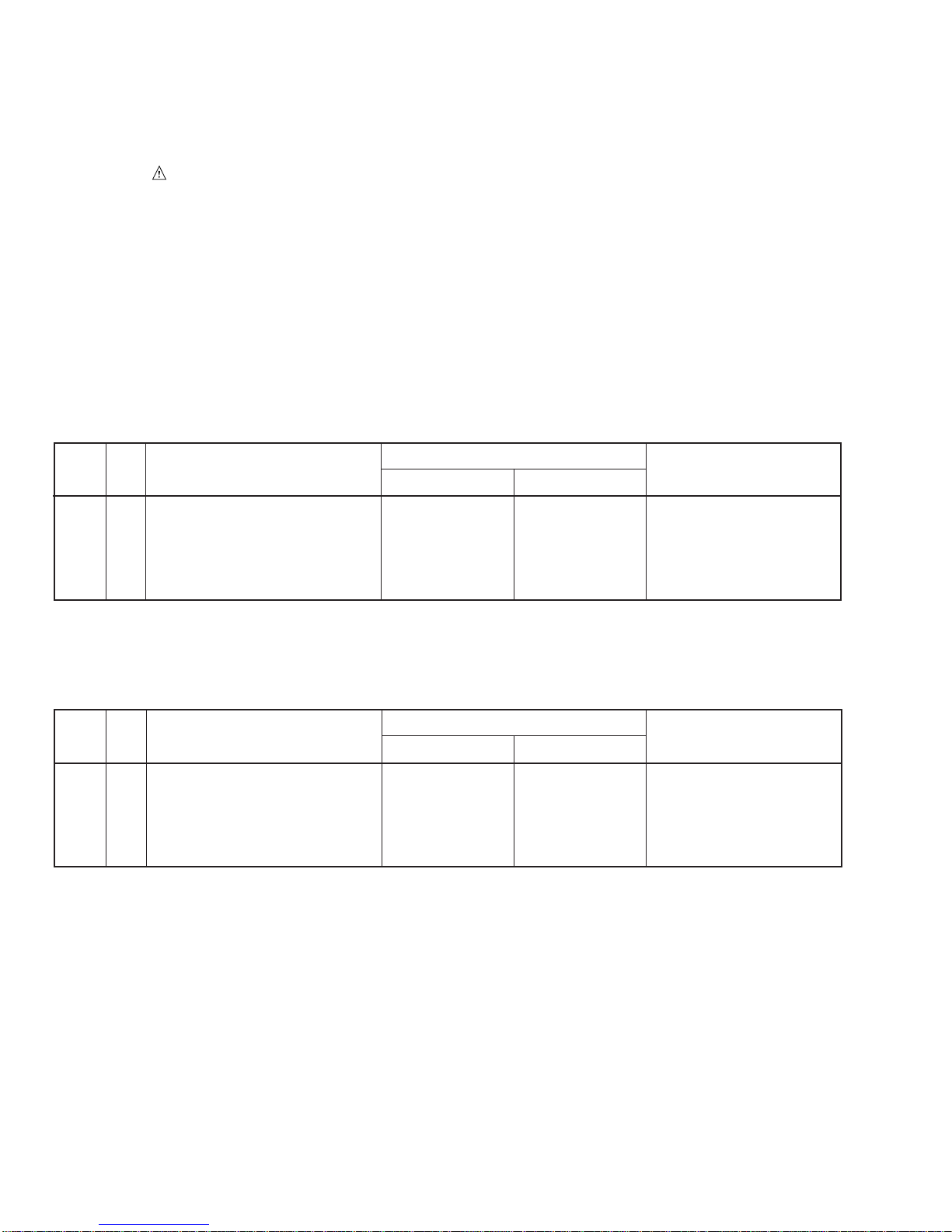
7CONTRAST TABLE FOR KU/CA2 TYPE
KU/CA2 type and KU/CA type are constructed the same except for the following:
ASSEMBLIES
P7– 8 DVDM ASSY VWS1377 VWS1397
BOTTOM VIEW SECTION
P9–29 REAR COVER VNA2028 VNA2144
Ref.
No. Remarks
KU/CA type KU/CA2 type
Part No.
Mark Symbol and Description
NOTES : ÷Parts marked by “ NSP ” are generally unavailable because they are not in our Master Spare Parts List.
÷The mark found on some component parts indicates the importance of the safety factor of the part.
Therefore, when replacing, be sure to use parts of identical designation.
÷Reference Nos. indicate the pages and Nos. in the service manual for the base model.
÷When ordering resistors, first convert resistance values into code form as shown in the following examples.
Ex. 1 When there are 2 effective digits (any digit apart from 0), such as 560 ohm and 47k ohm (tolerance is shown by
J = 5%, and K = 10%).
560 Ω=56 ×101 =561................................................... RD1/4PU 561J
47k Ω=47 ×10 3=473 .................................................. RD1/4PU 473J
0.5 Ω=R50 ...................................................................... RN2H Â50K
1 Ω=1R0 ......................................................................... RS1P 1Â0K
Ex. 2 When there are 3 effective digits (such as in high precision metal film resistors).
5.62k Ω=562 ×10 1=5621 ........................................... RN1/4PC 5621F
¶For PCB ASSEMBLIES, Refer to “CONTRAST OF PCB ASSEMBLIES”, “2. SCHEMATIC DIAGRAM” and “3. PCB CONNECTION DIAGRAM”.
7CONTRAST TABLE FOR RD/RA2 TYPE
RD/RA2 type and RD/RA type are constructed the same except for the following:
ASSEMBLIES
P7– 8 DVDM ASSY VWS1377 VWS1397
BOTTOM VIEW SECTION
LABEL Not used VRW1789 No. 1
Ref.
No. Remarks
RD/RA type RD/RA2 type
Part No.
Mark Symbol and Description
¶The numbers in the remarks column correspond to the numbers on the “EXPLODED VIEWS”.
¶For PCB ASSEMBLIES, Refer to “CONTRAST OF PCB ASSEMBLIES”, “2. SCHEMATIC DIAGRAM” and “3. PCB CONNECTION DIAGRAM”.


