stage (C) is reduced, and the reactanceof the in-
ductance stage (L) increased, resulting in AM
detection by D2 which leavesthe positive portion
of the IF signal. If the input frequency decreases,
L stagereactance is decreased
and C stagereact-
ance increased, resulting in AM detection by D1
which leaves
the negativeportion of the IF signal.
The L stage and C stage reactances increase as
the degreeof detuning in the respectivedirections
is increased,resulting in a subs€quent increase in
the detector output. By thus attaining S-cuwe
characteristics, FM detection becomes possible.
Since the IF signal is an FM signal frequency
deviation due to modulation it will be symmetrical
about a central axis. And if the central frequency
is equal to the resonancefrequency, the detector
output DC level will be zero. If, however, there is
any displacement in the central frequency, fre-
quency deviation in respect to the detector will
become asymmetrical, resulting in the generation
of a DC voltage. This DC voltage is passed
through
LPF1 (IF filter) and LPF2 (AC filter) to form a
correction voltage which is applied to the variable
capacitance diode in the local oscillator, thereby
correcting the oscillator frequency to obtain a
constant IF (i.e. a constant tuned frequency).
Since the central frequency of the crystal det€c-
tor is regulated by the crystal resonator, tuned fre-
quencies of extremely high stability are obtained.
r Limiting the t ocking Range
If the quartzJock range is too wide, it will
overlap with strong adjacent broadcastingfrequen-
cies and result in considerable tuning difficulties.
A DC amplifier is therefore used as a limiter
(limiter action by NFB circuit zenerdiodes)which
restricts the voltage applied to the variable capaci
tancediode, thereby limiting the quartz-lock range.
A DC voltage appears at pin no.13 of the IF
system IC (PA3007-A) when the antenna input
level drops below SpV, or when the tuned fre-
quency has been detuned by more than 1 100kHz.
This DC voltage (FM muting signal) is applied to
the gate of Q2 (FET) via a Schmitt circuit, result-
ing in the FET being turned on, and the quartz-
lock circuit beingtumed off .
4.2 AMTUNER
The AM tuner stage
employsa 2-gangedtuning
capacitor,
a singleclement
ceramicfilter, an NPN
transistor RF amplifier, a PNP transistormixer
(converter),
andanNPNtransistor
IF amplifier.
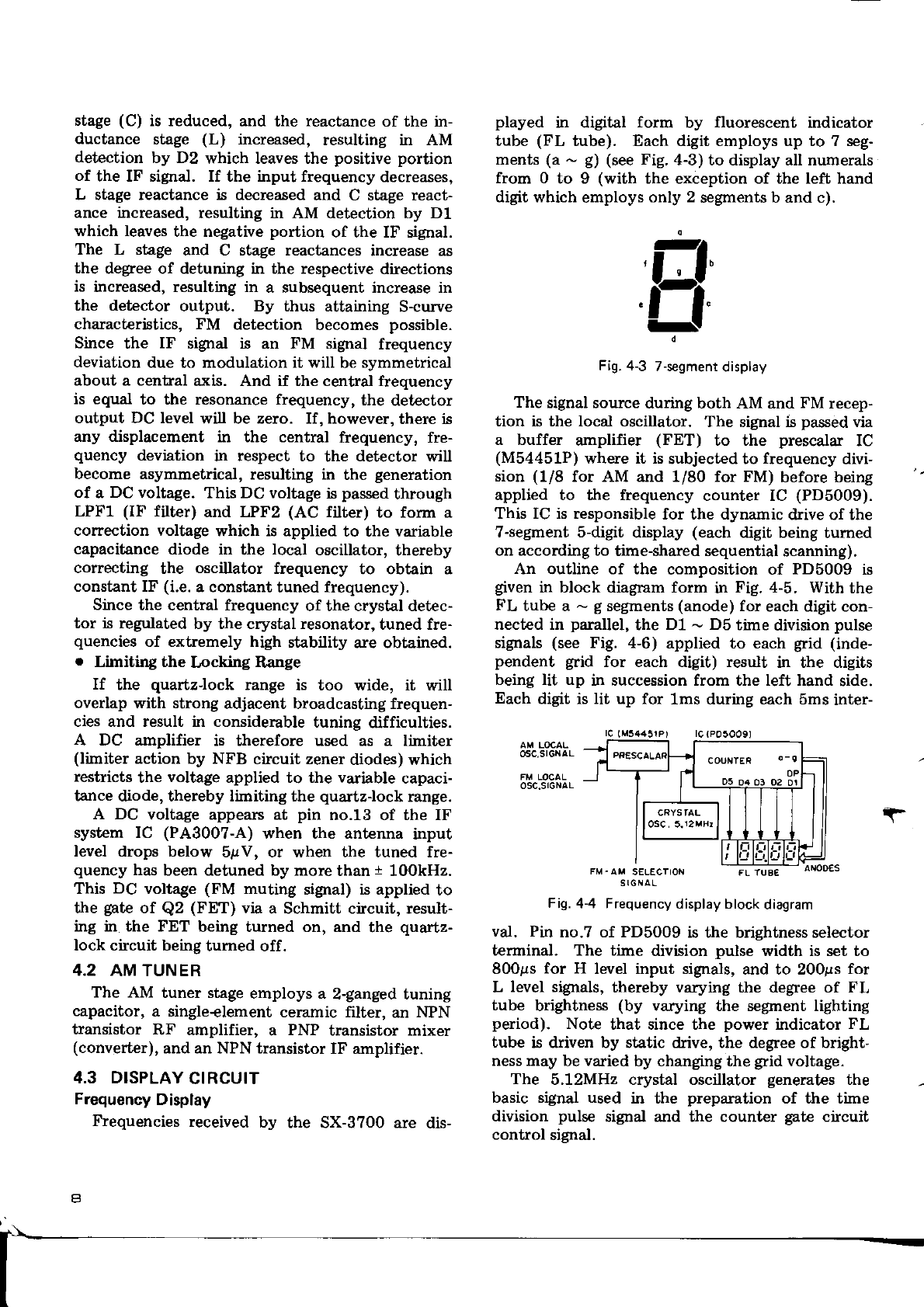
4.3 DISPLAY
CIRCUIT
Frequency
Display
Frequencies
received
by the SX-3700are dis-
played in digital form by fluorescent indicator
tube (FL tube). Each digit employs up to 7 seg-
ments (a - g) (seeFig. 4-3) to display all numerals
from 0 to 9 (with the exception of the left hand
digit which employs only 2 segmentsb and c).
Lt
ti
d
Fig.4-37-segment
display
The signalsourceduring both AM and FM recep-
tion is the local oscillator. The signalis passed
via
a buffer amplifier (FET) to the prescalar IC
(M54451P) where it is subjectedto frequency divi-
sion (1/8 for AM and 1/80 for FM) before being
applied to the frequency counter IC (PD5009).
This IC is responsible for the dynamic drive of the
?-segment 5-digit display (each digit being tumed
on accordingto time-sharedsequentialscanning).
An outline of the composition of PD5009 is
given in block diagram form in Fig. 4-5. With the
FL tube a - g segments
(anode) for eachdigit con-
nected in parallel, the D1 - D5 time division pulse
signals (see Fig. 4-6) applied to each grid (inde-
pendent grid for each digit) result in the digits
being lit up in successionfrom the left hand side.
Each digit is lit up for 1ms during each 5ms inter-
osc,sr6NAL
OSC.SIGNAL
sr.NAL FL luB€
Fig.
4-4 Frequency
displayblock
diagram
val. Pin no.7 of PD5009 is the brightnessselector
terminal. The time division pulse width is set to
8009s for H level input signals,and to 2009s for
L level signals,thereby varying the degree of FL
tube brightness (by varying the segmentlighting
period). Note that since the power indicator FL
tube is driven by static drive, the degreeof bright-
nessmay bevaried by changingthe grid voltage.
The 5.12MHz crystal oscillator generates the
basic signal used in the preparation of the time
division pulse signal and the counter gate circuit
control signal.
r