Profichip VPC3+ User manual

VPC3+ Evaluation Kit
(Order No.: PA006300)
Revision 2.00
The Clever Alternative

Liability Exclusion
We have tested the contents of this document regarding
agreement with the hardware and software described.
Nevertheless, there may be deviations and we do not
guarantee complete agreement. The data in the
document is tested periodically, however. Required
corrections are included in subsequent versions. We
gratefully accept suggestions for improvements.
Copyright
Copyright © profichip GmbH 2005. All Rights Reserved.
Unless permission has been expressly granted, passing
on this document or copying it, or using and sharing its
content are not allowed. Offenders will be held liable. All
rights reserved, in the event a patent is granted or a
utility model or design is registered.
This document is subject to technical changes.
ii Revision 2.00
VPC3+ Evaluation Kit
Copyright © profichip GmbH, 2005

Table of Contents
VPC3+ Evaluation Kit........................................................i
1Introduction.................................................................1
1.1 Overview ......................................................................................1
1.2 Document Conventions................................................................2
1.3 Handling the Boards.....................................................................2
2AT89C5132 Board .......................................................3
2.1 Overview ......................................................................................3
2.2 AT89C5132 board........................................................................4
2.3 AT89C5132..................................................................................5
2.4 In System Programming...............................................................5
2.5 Address Map................................................................................5
2.6 Internal/External Clock (Jumper X6) ............................................6
2.7 Display Elements..........................................................................6
2.8 I/O Area........................................................................................6
2.9 Reset Button S4...........................................................................6
2.10 RS232 Interface ...........................................................................7
2.11 LCD..............................................................................................7
2.12 RTC..............................................................................................7
2.13 MMC.............................................................................................7
2.14 I2C................................................................................................7
2.15 Connector.....................................................................................8
2.15.1 Users Board Connector ( X4 ) ..........................................8
2.15.2 MPI Board ( Main Connector, X5 )....................................9
2.15.3 MPI Board ( Extension Connector, X9 )..........................10
2.16 Power Supply.............................................................................11
2.17 Technical Data ...........................................................................12
3VPC3+/C Extension Board .......................................13
3.1 Overview ....................................................................................13
3.2 Board VPC3+/C..........................................................................14
3.3 Jumpers......................................................................................15
3.3.1 VPC3+/C microcontroller mode......................................15
3.3.2 VPC3+/C clock divider....................................................15
3.3.3 Select PROFIBUS interface............................................16
3.3.4 Select Opto/ADuM Interface...........................................16
3.4 Connectors.................................................................................17
3.4.1 Testpins X13...................................................................17
3.4.2 Main Connector X14.......................................................17
3.4.3 Extension Connector X14...............................................18
3.5 Display Elements........................................................................19
3.6 PROFIBUS Interfaces................................................................19
3.6.1 RS485 Interface..............................................................19
3.6.2 Fiber Optic Interface.......................................................20
3.7 Technical Data ...........................................................................22
4Schematics................................................................23
VPC3+ Evaluation Kit Revision 2.00 iii
Copyright © profichip GmbH, 2005

Table of Contents
4.1 AT89C5132................................................................................23
4.2 VPC3+/C Extension Board.........................................................28
5ISP (InSystemProgramming)....................................33
5.1 ATMEL FLIP 2.4.4......................................................................33
5.2 How to use FLIP.........................................................................34
iv Revision 2.00
VPC3+ Evaluation Kit
Copyright © profichip GmbH, 2005

Introduction 1
1 Introduction
1.1 Overview
Profichip's VPC3+ Evaluation Kit contains all the necessary hardware and
software to easily connect to PROFIBUS-DP.
It consists of:
Controller board with Atmel 89C5132 microcontroller
8-bit MCU C51 Core-based (FMAX = 20 MHz)
2304 Bytes of Internal RAM
64K Bytes of Code Memory (Flash)
USB Rev 1.1 Device Controller
32kByte external RAM
RS232 interface
LCD-display
Real Time Clock
wide range of power supply (DC 7-24V)
all relevant signals are applied to the plug connectors
DIP-switches and LED's
VPC3+/C extension board
PROFIBUS link via RS485
PROFIBUS link via fiber optic interface
VPC3+ configurations are done with jumpers
all relevant signals are applied to the plug connectors
PROFIBUS software driver
DPV0 software driver
DPV1 software driver
PROFIBUS demo program
DPV1AFFE: demo program for DPV1
DPV0AFFE: demo program for DPV0
Documentation
VPC3+ Evaluation Kit Revision 2.00 1
Copyright © profichip GmbH, 2005

1 Introduction
1.2 Document Conventions
In this User Description signal names appear in italic.
Low active signals are denoted by a "#" after the signal name (i.e.: RD#).
A '0' indicates a logic-zero or low-level signal, while a '1' represents a logic-
one or high-level signal.
1.3 Handling the Boards
Handle the VPC3+ evaluation boards with care in respect to ESD require-
ments. Take precautions to use the boards only at an ESD-safe workplace.
2 Revision 2.00
VPC3+ Evaluation Kit
Copyright © profichip GmbH, 2005

AT89C5132 Board 2
2 AT89C5132 Board
2.1 Overview
The AT89C5132 board consist of:
Atmel 89C5132 microcontroller (USB C51-based Microcontroller with
64K Bytes Flash, 2304 bytes RAM, 4 USB Endpoints, SPI, UART, IDE,
TWI, MultiMediaCard, DataFlash, I2S, 10-bit ADC)
32kByte external RAM
RS232 interface
LCD-display
Real Time Clock
wide range of power supply (DC 7-24V)
all relevant signals are applied to the plug connectors
DIP-switches and LED's
VPC3+ Evaluation Kit Revision 2.00 3
Copyright © profichip GmbH, 2005

2 AT89C5132 Board
2.2 AT89C5132 board
Figure 2-1: AT89C5132
4 Revision 2.00
VPC3+ Evaluation Kit
Copyright © profichip GmbH, 2005

AT89C5132 Board 2
2.3 AT89C5132
USB C51-based Microcontroller with 64K Bytes Flash, 2304 bytes RAM, 4
USB Endpoints, SPI, UART, IDE, TWI, MultiMediaCard, DataFlash, I2S,
10-bit ADC. The functionality of AT89C5132 is described more detailed in
the document 4173.pdf.
2.4 In System Programming
The ISP area contains a switch that allows the user to select the
AT89C5132 hardware condition and thus execute the embedded
bootloader or to run the client application.
ISP Position Execute
Client Application
ISP Bootloader
Figure 2-2: Switch S2, ISP
2.5 Address Map
Fehler! Verweisquelle konnte nicht gefunden werden. shows the
address mapping of the AT89C5132 controller board.
Address Description
0000 – 7FFFH External RAM
8000 – 8FFFH VPC3+/C
9000 – 9FFFH Reserved
A000 – AFFFH FPGA on VPC3+/C Base Board
B000 – BFFFH RTC
C000 – CFFFH LCD
D000 – DFFFH I/O Port 0
E000 – EFFFH I/O Port 1
F000 – FFFFH I/O Port 2
Figure 2-3: Address Map
VPC3+ Evaluation Kit Revision 2.00 5
Copyright © profichip GmbH, 2005

2 AT89C5132 Board
2.6 Internal/External Clock (Jumper X6)
The clock supply of the microcontroller can be determined by setting the
jumper X6. There are two possibilities for the controller's clock supply: The
controller can either get it's clock from the 20 MHz crystal oscillator on the
AT89C5132 board (Internal Clock) or from the CLKOUT2/4 pin of the VPC
3+ on the Extension board (External Clock):
Default
External Clock
Internal Clock (Default)
Figure 2-4: Settings of Jumper X6
2.7 Display Elements
The Extension Board has three LEDs: The green LED D10 indicates
correct power supply. The red LED D9 and the yellow LED D8 are
connected to the ports P1.4 and P1.5 of the controller.
2.8 I/O Area
The I/O area consist of 3 DIP switches (Port0, Port1, Port2) and 3 LED
lines.
The data bus lines to the DIP switches are connected via pulldown resistors
to GND. If a DIP switch is OFF, the corresponding input port of the
controller is connected via pulldown resistor to GND and the controller
therefore reads a logical '0' from this DIP-switch. If the DIP-switch is ON,
the controller's input is connected to VCC via the DIP-switch and the
controller therefore reads a logical '1' on this port.
2.9 Reset Button S4
The entire application can be reseted by pressing the Reset Button S4.The
microcontroller goes into a defined state and starts up the application
program.
6 Revision 2.00
VPC3+ Evaluation Kit
Copyright © profichip GmbH, 2005
AT89C5132 Board 2
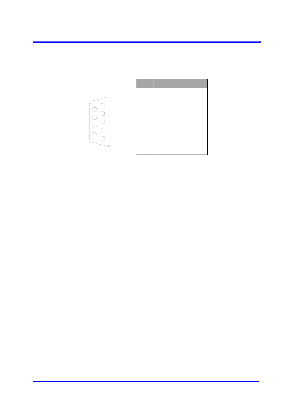
2.10 RS232 Interface
Pin Assignment
1
2
3
4
5
6
7
8
9
1
2
3
4
5
6
7
8
9
n.c.
TxD
RxD
n.c.
GND
n.c.
RTS
CTS
n.c.
Figure 2-5: Assignment of the RS232 Connector
2.11 LCD
The display area consist of a 2-line 20 characters LCD-display. The
contrast is adjustable using R3 variable resistor. The LCD is described
more detailed in the document
2.12 RTC The V3022 is a low power CMOS real time clock with a built-in crystal. The
interface is 8 bits with multiplexed address and data bus. Multiplexing of
address and data is handled by the input line /D. The RTC is described
more detailed in the document V3022_DS.pdf.
2.13 MMC
Multi Media Card is not supported.
2.14 I2C I2C is not supported
VPC3+ Evaluation Kit Revision 2.00 7
Copyright © profichip GmbH, 2005

2 AT89C5132 Board
2.15 Connector
2.15.1 Users Board Connector ( X4 )
Pin Signal name In/Out Description
1 GND Out GND
30 GND Out GND
32 GND Out GND
34 GND Out GND
2 VCC Out +5V
33 VCC Out +5V
29 VCC_3.3V Out +3.3V
31 VCC_3.3V Out +3.3V
3 AD0 In/Out Address / Data line 0
5 AD1 In/Out Address / Data line 1
7 AD2 In/Out Address / Data line 2
9 AD3 In/Out Address / Data line 3
11 AD4 In/Out Address / Data line 4
13 AD5 In/Out Address / Data line 5
15 AD6 In/Out Address / Data line 6
17 AD7 In/Out Address / Data line 7
4 A8 Out Address line 8
6 A9 Out Address line 9
8 A10 Out Address line 10
10 A11 Out Address line 11
12 A12 Address line 12
14 A13 Address line 13
16 A14 Address line 14
18 A15 Address line 15
19 RD# Out Read select
21 WR# Out Write select
23 ALE Out Address latch enable
26 RES Out Reset
27 EXT_CLK In External clock
28 CS_EXT0# Out Chip select
20 Not connected
22 Not connected
24 Not connected
25 Not connected
Figure 2-6: Assignment of Connector X5
8 Revision 2.00
VPC3+ Evaluation Kit
Copyright © profichip GmbH, 2005

AT89C5132 Board 2
2.15.2 MPI Board ( Main Connector, X5 )
Pin Signal name In/Out Description
1 GND Out GND
12 GND Out GND
14 GND Out GND
16 GND Out GND
18 GND Out GND
20 GND Out GND
22 GND Out GND
34 GND Out GND
2 VCC Out +5V
33 VCC Out +5V
3 AD0 In/Out Address / Data line 0
5 AD1 In/Out Address / Data line 1
7 AD2 In/Out Address / Data line 2
9 AD3 In/Out Address / Data line 3
11 AD4 In/Out Address / Data line 4
13 AD5 In/Out Address / Data line 5
15 AD6 In/Out Address / Data line 6
17 AD7 In/Out Address / Data line 7
4 A8 Out Address line 8
6 A9 Out Address line 9
8 A10 Out Address line 10
10 CS# Out Chip select for the VPC3+
19 RD# Out Read select
21 WR# Out Write select
23 ALE Out Address latch enable
24 INT_CI# In Interrupt output
25 INT_EV# In Interrupt output
26 RES_MPI12x Out Reset for VPC3+
27 EXT_CLK In VPC3+ clock output, 12 MHz or 24 MHz
28 CS_EXT0# Out Chip select for DIP-switches and LEDs
31 DIR_AB# Out Direction reverser for the fibre optic interface
32 EN_LWL_B Out Enable signal for fibre optic interface B
29 A11 Out Address line 11
30 Not connected
Figure 2-7: Assignment of Connector X5
VPC3+ Evaluation Kit Revision 2.00 9
Copyright © profichip GmbH, 2005

2 AT89C5132 Board
2.15.3 MPI Board ( Extension Connector, X9 )
Pin Signal name In/Out Description
1 GND Out GND
18 GND Out GND
22 GND Out GND
2 24V_OUT Out +24V
17 VCC_3.3V Out +3.3V
21 VCC_3.3V Out +3.3V
3 A10 Out Address line 10
4 A11 Out Address line 11
5 A12 Out Address line 12
6 A13 Out Address line 13
7 A14 Out Address line 14
8 A15 Out Address line 15
10 HLDTOK# In Hold Token
12 INT_FPGA In Interrupt FPGA
9 CS_FPGA’ Out Chip select FPGA
11 FPGA_PROG# Out
13 FPGA_CCLK Out
15 FPGA_DIN Out
14 FPGA_INIT# In
16 FPGA_DONE Out
FPGA
20 RES# Out Reset
19 Not connected
Figure 2-8: Assignment of Connector X9
10 Revision 2.00
VPC3+ Evaluation Kit
Copyright © profichip GmbH, 2005
AT89C5132 Board 2
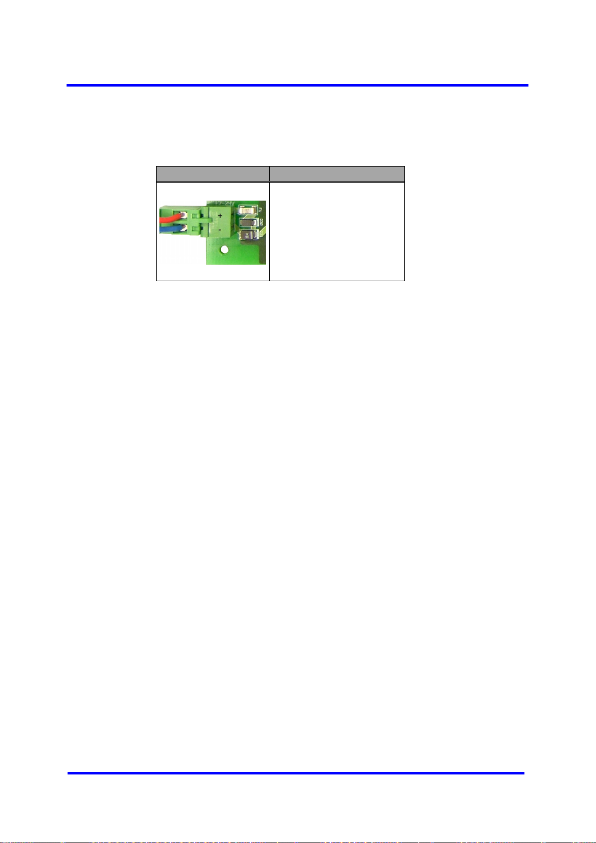
2.16 Power Supply
7V-24V DC, from external
power supply
Figure 2-9: Power Supply
VPC3+ Evaluation Kit Revision 2.00 11
Copyright © profichip GmbH, 2005

2 AT89C5132 Board
2.17 Technical Data
Electrical data C501 Extension Board
Power supply 7V – 24V DC, from ext. power supply
Current consumption
Operating temperature 0°C to +70°C
Dimensions and Weight
Dimensions (LxWxH) 89mm x 180mm x 16mm
Weight
Figure 2-10 : Technical data
12 Revision 2.00
VPC3+ Evaluation Kit
Copyright © profichip GmbH, 2005

VPC3+/C Extension Board 3
3 VPC3+/C Extension Board
3.1 Overview
The extension board contains all necessary hardware to connect to
PROFIBUS:
VPC3+/C slave ASIC
48 MHz clock generator
RS485 interface
realized with opto coupler
realized with ADuM
electrical isolation
fiber optic interface
FPGA (for internal use)
VPC3+ Evaluation Kit Revision 2.00 13
Copyright © profichip GmbH, 2005

3 VPC3+/C Extension Board
3.2 Board VPC3+/C
Figure 3-1: Extension Board VPC3+/C
14 Revision 2.00
VPC3+ Evaluation Kit
Copyright © profichip GmbH, 2005

VPC3+/C Extension Board 3
3.3 Jumpers
3.3.1VPC3+/C microcontroller mode
Jumper X16 selects the VPC3+ microcontroller mode:
Mode Default setting Interface
asynchron Intel
synchron Motorola
Figure 3-2: VPC3+/C microcontroller mode
3.3.2VPC3+/C clock divider
Jumper X17 selects the VPC3+/C CLK to CLKOUT2/4 divider:
Default Default setting
Divider 0: CLK divided by 4
Divider 1: CLK divided by 2
Figure 3-3: VPC3+/C clock divider
VPC3+ Evaluation Kit Revision 2.00 15
Copyright © profichip GmbH, 2005
3 VPC3+/C Extension Board
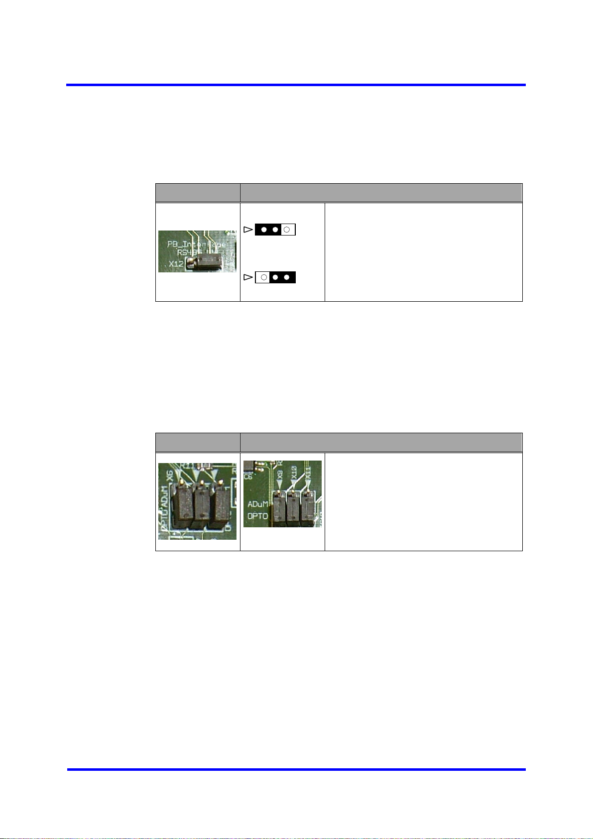
3.3.3Select PROFIBUS interface
Jumper X12 selects the PROFIBUS interface to be used (the print on the
PCB is wrong):
Default (RS485) Interface
Fiber optic interface
RS485 PROFIBUS interface (DEFAULT)
Figure 3-4: PROFIBUS interface
3.3.4Select Opto/ADuM Interface
Jumper X6..X11 selects the Opto/ADuM interface:
Default (RS485) Interface
ADuM interface
OPTO interface (DEFAULT)
Figure 3-5: PROFIBUS interface
16 Revision 2.00
VPC3+ Evaluation Kit
Copyright © profichip GmbH, 2005
This manual suits for next models
1
Table of contents
Other Profichip Motherboard manuals

Popular Motherboard manuals by other brands

Intel
Intel D102GGC2 quick reference

Linear Technology
Linear Technology LT1765EFE quick start guide

Texas Instruments
Texas Instruments Stellaris EK-LM3S9B92 user manual

American Megatrends
American Megatrends Super Voyager LPX user guide

Gigabyte
Gigabyte X570S AORUS PRO AX user manual

Texas Instruments
Texas Instruments LM61460EVM user guide


