Alinx AXKU040 User manual

KINTEX UltraScale FPGA
Development Board
AXKU040
User Manual

KINTEX UltraScale+ FPGA Board AXKU040 User Manual
2 / 59
www.alinx.com
Version Record
Version
Date
Release By
Description
Rev 1.1
2021-09-13
Rachel Zhou
First Release

KINTEX UltraScale+ FPGA Board AXKU040 User Manual
3 / 59
www.alinx.com
Table of Contents
Version Record.......................................................................................................2
Part 1: FPGA Development Board Introduction............................................... 4
Part 2: FPGA Chip................................................................................................. 8
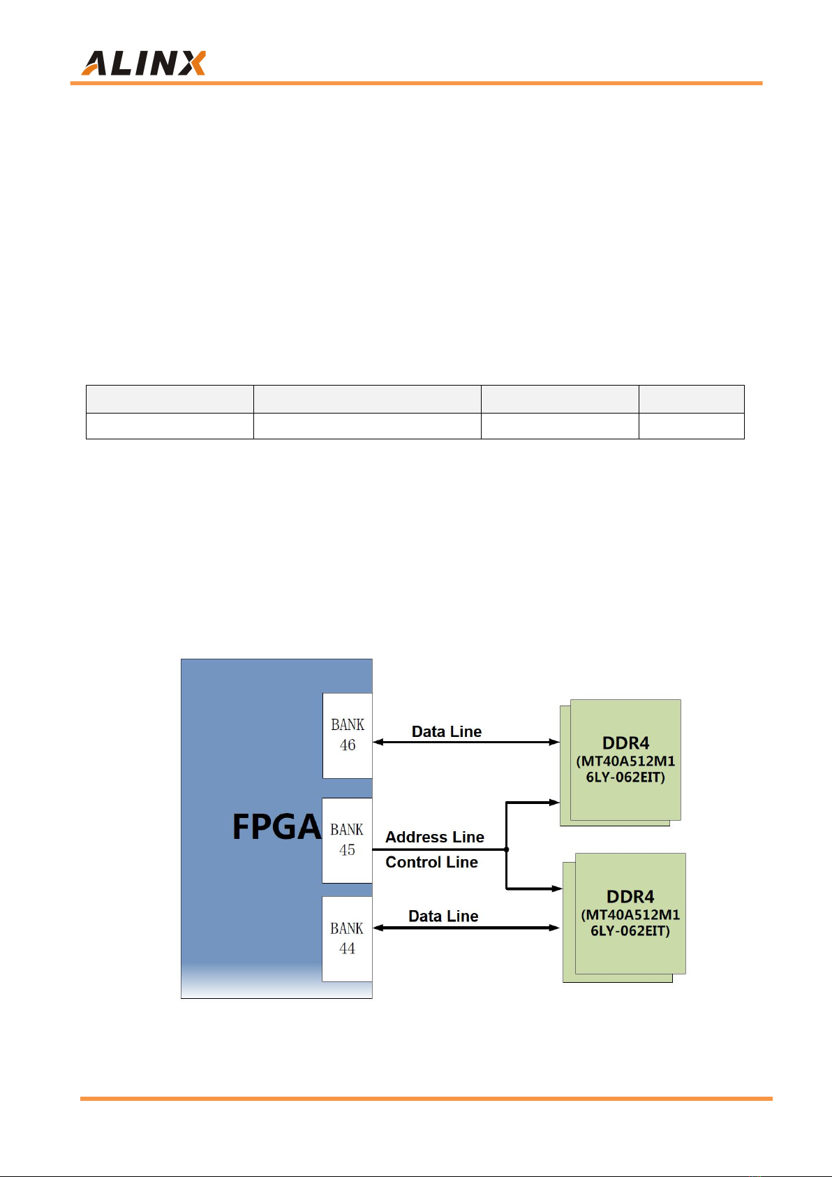
Part 3: DDR4 DRAM...........................................................................................10
Part 4: QSPI Flash.............................................................................................. 15
Part 5: Clock configuration.................................................................................16
Part 5.1: 200Mhz differential clock source..............................................16
Part 5.2: 125Mhz differential clock source..............................................16
Part 5.3: 156.25Mhz differential clock source........................................17
Part 6: USB to Serial Port.................................................................................. 19
Part 7: SFP+ Optical fiber interface................................................................. 20
Part 8: HDMI Video Output Interface............................................................... 22
Part 9: Gigabit Ethernet Interface.....................................................................24
Part 10: FMC Expansion Port........................................................................... 27
Part 11: SD Card Slot......................................................................................... 47
Part 12: SMA and SATA Interface.....................................................................49
Part 13: Temperature Sensor............................................................................ 51
Part 14: JTAG Interface......................................................................................52
Part 15: LED Light...............................................................................................53
Part 16: Keys........................................................................................................55
Part 17: Power Supply........................................................................................56
Part 18: Fan..........................................................................................................58
Part 19: Form Factory.........................................................................................59

KINTEX UltraScale+ FPGA Board AXKU040 User Manual
4 / 59
www.alinx.com
Part 1: FPGA Development Board Introduction
The AXKU040 FPGA development board is mainly composed of KINTEX
UltraScale+ chip. It meets users' requirements for high-speed data exchange,
data storage, Video transmission processing, deep learning, artificial
intelligence and industrial control, and it is a "professional" FPGA development
platform. For high-speed data transmission and exchange, pre-verification and
post-application of data processing is possible. This product is very suitable for
students, engineers and other groups engaged in FPGA development.
AXKU040 FPGA development board mounts four 1GB high-speed DDR4
SDRAM chips. FPGA chip configuration uses a 128Mb QSPI FLASH chip.
The AXKU040 FPGA development board expands the rich peripheral
interface, including four 10G optical SFP interfaces, three FMC expansion
interfaces, one UART serial interface, one SD card interface, one HDMI Output,
2 Gigabit Ethernet Interfaces, SAM and SATA Interfaces etc.
The following figure shows the structure of the entire development system:
Figure 1-1: The Schematic Diagram of the AXKU040

KINTEX UltraScale+ FPGA Board AXKU040 User Manual
5 / 59
www.alinx.com
Through this diagram, you can see the interfaces and functions that the
AXKU040 FPGA Development Board contains:
Xilinx KINTEX-7 UltraScale FPGA chip XCKU040
DDR4
With four large-capacity 1GB (4 GB total) high-speed DDR4 SDRAM,
used as FPGA data storage, image analysis cache, data processing.
QSPI FLASH
A 128Mbit QSPI FLASH memory chip can be used as a storage for
FPGA chip configuration files and user data;
4 SFP+ interfaces
The four high-speed transceivers of the GTX transceiver of the FPGA
are connected to the transmission and reception of four optical modules
to realize four high-speed optical fiber communication interfaces. Each
fiber optic data communication receives and transmits at speeds of up
to 12.5 Gb/s.
USB Uart interface
1-channel Uart to USB interface for communication with the computer
for user debugging. The serial port chip adopts the USB-UAR chip of
Silicon Labs CP2102GM, and the USB interface adopts the MINI USB
interface.
HDMI Output Interface
1 HDMI video output interface, using ADV7511 HDMI encoding chip
from ANALOG DEVICE, supports up to 1080P@60Hz output and 3D
output.
Gigabit Ethernet Interface
2-Channel 10/100M/1000M Ethernet RJ45 interface for Ethernet data
exchange with computers or other network devices. The network
interface chip uses Micrel's KSZ9031 industrial grade GPHY chip.
FMC Expansion Interface

KINTEX UltraScale+ FPGA Board AXKU040 User Manual
6 / 59
www.alinx.com
3 standard FMC expansion port, including 2 LPC FMC expansion ports
and 1 HPC FMC expansion port, which can be connected to various
FMC modules of XILINX or ALINX (HDMI input and output modules,
binocular camera modules, high-speed AD modules, etc.).
Micro SD slot
1 Micro SD card holder, used to store operating system image and file
system.
SMA Interface and SATA Interfaces
6 SMA external interfaces and 2 SATA interfaces, the pins are
connected to the transceiver for external high-speed input and output
signals.
Temperature and humidity sensor
Onboard a temperature and humidity sensor chip LM75 for detecting
the temperature and humidity of the environment around the board
EEPROM
One EEPROM 24LC04 with I2C interface, which is Used for IIC bus
communication and storage of some customer-defined information.
JTAG Interface
A 10-pin0.1 spacing standard JTAG ports for FPGA program download
and debugging. Users can debug and download FPGAs through
XILINX downloader.
Clock
A 200Mhz differential crystal onboard provides a stable clock source for
the FPGA system.
A 125Mhz differential crystal onboard provides reference clock for
optical fiber.
A 156.25Mhz differential crystal onboard provides reference clock for
transceiver

KINTEX UltraScale+ FPGA Board AXKU040 User Manual
7 / 59
www.alinx.com
LED Light
6LEDs, 1 power indicator, 1 DONE configuration indicator, 4 user
indicators
Key
2 user keys, 1 reset key, connect to the normal IO of the FPGA.

KINTEX UltraScale+ FPGA Board AXKU040 User Manual
8 / 59
www.alinx.com
Part 2: FPGA Chip
The FPGA development board uses Xilinx's KINTEX UltraScale FPGA
chip, model number XCKU040-2FFVA1156I. The speed class is 2 and the
temperature class is industrial. This model is a FFVA1156 package with 1156
pins and a 1.0mm pitch. The chip naming rules for Xilinx KINTEX UltraScale
FPGA are shown in Figure 2-1 below:
Figure 2-1: The Chip Model Definition of KINTEX UltraScale Series
The main parameters of the FPGA chip XCKU040 are as follows
Name
Specific parameters
Logic Cells
530,250
CLB Look-Up-Tables
242,400
CLB flip-flops
41,600
Block RAM(kb)
21.1
DSP Slices
1,920
PCIe Gen3 x 8
3
XADC
12bit, 1Mbps AD
GTP Transceiver
20, 16.3Gb/s max
Speed Grade
-2
Temperature Grade
Industrial

KINTEX UltraScale+ FPGA Board AXKU040 User Manual
9 / 59
www.alinx.com
FPGA power supply system
XCKU040 FPGA power supplies are VCCINT, VCCBRAM, VCCAUX, VCCAUX_IO VCCO,
VMGTAVCC , VMGTAVTT, VMGTVCCAUK , VMGTAVTTRCAL, VCCADC. VCCINT is the FPGA core power
supply pin, which needs to be connected to 0.95V; VCCBRAM is the power supply
pin of FPGA Block RAM, connect to 0.95V; VCCAUX and VCCAUX_IO are FPGA
auxiliary power supply pin, connect 1.8V; VCCO is the voltage of each BANK of
FPGA, including BANK0, BANK44~48, BANK64~68. VMGTAVCC is the power
supply voltage of the GTH and GTY transceivers inside the FPGA, connected
to 1.0V; VMGTAVTT is the terminal voltage of GTH transmission and reception,
connected to 1.2V. VMGTAVTTRCAL is the transceiver resistance calibration voltage,
connect to 1.2V. VCCADC is the supply voltage of XADC, connected to 1.8V.
The XCKU040 FPGA system requires the power-on sequence as shown in
Figure 2-2.
Figure 2-2: Power-On/Off Power Supply Sequencing

KINTEX UltraScale+ FPGA Board AXKU040 User Manual
10 / 59
www.alinx.com
Part 3: DDR4 DRAM
The AXKU040 FPGA development board is equipped with four Micron
1GB DDR4 chips, model MT40A512M16LY-062EIT. Four DDR4 SDRAMs
form a 64-bit bus width. Because four DDR4 chips are connected to the FPGA,
the DDR4 SDRAM can run at speeds up to 1200MHz, and four DDR4 memory
systems are directly connected to the BANK44, BANK45, and BANK46
interfaces of the FPGA. The specific configuration of DDR4 SDRAM is shown
in Table 3-1.
Bit Number
Chip Model
Capacity
Factory
U45,U47,U48,U49
MT40A512M16LY-062EIT
512M x 16bit
Micron
Table 3-1: DDR4 SDRAM Configuration
The hardware design of DDR4 requires strict consideration of
signal integrity. We have fully considered the matching resistor/terminal
resistance, trace impedance control, and trace length control in circuit
design and PCB design to ensure high-speed and stable operation of
DDR3.
Figure 3-1: The DDR4 DRAM Schematic

KINTEX UltraScale+ FPGA Board AXKU040 User Manual
11 / 59
www.alinx.com
4 DDR4 DRAM pin assignments:
Signal Name
FPGA Pin Name
FPGA Pin
PL_DDR4_DQ0
IO_L3N_T0L_N5_AD15N_44
AE20
PL_DDR4_DQ1
IO_L2N_T0L_N3_44
AG20
PL_DDR4_DQ2
IO_L2P_T0L_N2_44
AF20
PL_DDR4_DQ3
IO_L5P_T0U_N8_AD14P_44
AE22
PL_DDR4_DQ4
IO_L3P_T0L_N4_AD15P_44
AD20
PL_DDR4_DQ5
IO_L6N_T0U_N11_AD6N_44
AG22
PL_DDR4_DQ6
IO_L6P_T0U_N10_AD6P_44
AF22
PL_DDR4_DQ7
IO_L5N_T0U_N9_AD14N_44
AE23
PL_DDR4_DQ8
IO_L8N_T1L_N3_AD5N_44
AF24
PL_DDR4_DQ9
IO_L11P_T1U_N8_GC_44
AJ23
PL_DDR4_DQ10
IO_L8P_T1L_N2_AD5P_44
AF23
PL_DDR4_DQ11
IO_L12N_T1U_N11_GC_44
AH23
PL_DDR4_DQ12
IO_L9N_T1L_N5_AD12N_44
AG25
PL_DDR4_DQ13
IO_L11N_T1U_N9_GC_44
AJ24
PL_DDR4_DQ14
IO_L9P_T1L_N4_AD12P_44
AG24
PL_DDR4_DQ15
IO_L12P_T1U_N10_GC_44
AH22
PL_DDR4_DQ16
IO_L14P_T2L_N2_GC_44
AK22
PL_DDR4_DQ17
IO_L17P_T2U_N8_AD10P_44
AL22
PL_DDR4_DQ18
IO_L15N_T2L_N5_AD11N_44
AM20
PL_DDR4_DQ19
IO_L17N_T2U_N9_AD10N_44
AL23
PL_DDR4_DQ20
IO_L14N_T2L_N3_GC_44
AK23
PL_DDR4_DQ21
IO_L18N_T2U_N11_AD2N_44
AL25
PL_DDR4_DQ22
IO_L15P_T2L_N4_AD11P_44
AL20
PL_DDR4_DQ23
IO_L18P_T2U_N10_AD2P_44
AL24
PL_DDR4_DQ24
IO_L20P_T3L_N2_AD1P_44
AM22
PL_DDR4_DQ25
IO_L23P_T3U_N8_44
AP24
PL_DDR4_DQ26
IO_L20N_T3L_N3_AD1N_44
AN22
PL_DDR4_DQ27
IO_L21N_T3L_N5_AD8N_44
AN24
PL_DDR4_DQ28
IO_L24P_T3U_N10_44
AN23
PL_DDR4_DQ29
IO_L23N_T3U_N9_44
AP25
PL_DDR4_DQ30
IO_L24N_T3U_N11_44
AP23
PL_DDR4_DQ31
IO_L21P_T3L_N4_AD8P_44
AM24
PL_DDR4_DQ32
IO_L2P_T0L_N2_46
AM26
PL_DDR4_DQ33
IO_L6P_T0U_N10_AD6P_46
AJ28

KINTEX UltraScale+ FPGA Board AXKU040 User Manual
12 / 59
www.alinx.com
PL_DDR4_DQ34
IO_L2N_T0L_N3_46
AM27
PL_DDR4_DQ35
IO_L6N_T0U_N11_AD6N_46
AK28
PL_DDR4_DQ36
IO_L5P_T0U_N8_AD14P_46
AH27
PL_DDR4_DQ37
IO_L5N_T0U_N9_AD14N_46
AH28
PL_DDR4_DQ38
IO_L3P_T0L_N4_AD15P_46
AK26
PL_DDR4_DQ39
IO_L3N_T0L_N5_AD15N_46
AK27
PL_DDR4_DQ40
IO_L9N_T1L_N5_AD12N_46
AN28
PL_DDR4_DQ41
IO_L12N_T1U_N11_GC_46
AM30
PL_DDR4_DQ42
IO_L8P_T1L_N2_AD5P_46
AP28
PL_DDR4_DQ43
IO_L11N_T1U_N9_GC_46
AM29
PL_DDR4_DQ44
IO_L9P_T1L_N4_AD12P_46
AN27
PL_DDR4_DQ45
IO_L12P_T1U_N10_GC_46
AL30
PL_DDR4_DQ46
IO_L11P_T1U_N8_GC_46
AL29
PL_DDR4_DQ47
IO_L8N_T1L_N3_AD5N_46
AP29
PL_DDR4_DQ48
IO_L14P_T2L_N2_GC_46
AK31
PL_DDR4_DQ49
IO_L18P_T2U_N10_AD2P_46
AH34
PL_DDR4_DQ50
IO_L14N_T2L_N3_GC_46
AK32
PL_DDR4_DQ51
IO_L15N_T2L_N5_AD11N_46
AJ31
PL_DDR4_DQ52
IO_L15P_T2L_N4_AD11P_46
AJ30
PL_DDR4_DQ53
IO_L17P_T2U_N8_AD10P_46
AH31
PL_DDR4_DQ54
IO_L18N_T2U_N11_AD2N_46
AJ34
PL_DDR4_DQ55
IO_L17N_T2U_N9_AD10N_46
AH32
PL_DDR4_DQ56
IO_L21P_T3L_N4_AD8P_46
AN31
PL_DDR4_DQ57
IO_L24P_T3U_N10_46
AL34
PL_DDR4_DQ58
IO_L23N_T3U_N9_46
AN32
PL_DDR4_DQ59
IO_L20P_T3L_N2_AD1P_46
AN33
PL_DDR4_DQ60
IO_L23P_T3U_N8_46
AM32
PL_DDR4_DQ61
IO_L24N_T3U_N11_46
AM34
PL_DDR4_DQ62
IO_L21N_T3L_N5_AD8N_46
AP31
PL_DDR4_DQ63
IO_L20N_T3L_N3_AD1N_46
AP33
PL_DDR4_DM0
IO_L1P_T0L_N0_DBC_44
AD21
PL_DDR4_DM1
IO_L7P_T1L_N0_QBC_AD13P_44
AE25
PL_DDR4_DM2
IO_L13P_T2L_N0_GC_QBC_44
AJ21
PL_DDR4_DM3
IO_L19P_T3L_N0_DBC_AD9P_44
AM21
PL_DDR4_DM4
IO_L1P_T0L_N0_DBC_46
AH26
PL_DDR4_DM5
IO_L7P_T1L_N0_QBC_AD13P_46
AN26

KINTEX UltraScale+ FPGA Board AXKU040 User Manual
13 / 59
www.alinx.com
PL_DDR4_DM6
IO_L13P_T2L_N0_GC_QBC_46
AJ29
PL_DDR4_DM7
IO_L19P_T3L_N0_DBC_AD9P_46
AL32
PL_DDR4_DQS0_P
IO_L4P_T0U_N6_DBC_AD7P_44
AG21
PL_DDR4_DQS0_N
IO_L4N_T0U_N7_DBC_AD7N_44
AH21
PL_DDR4_DQS1_P
IO_L10P_T1U_N6_QBC_AD4P_44
AH24
PL_DDR4_DQS1_N
IO_L10N_T1U_N7_QBC_AD4N_44
AJ25
PL_DDR4_DQS2_P
IO_L16P_T2U_N6_QBC_AD3P_44
AJ20
PL_DDR4_DQS2_N
IO_L16N_T2U_N7_QBC_AD3N_44
AK20
PL_DDR4_DQS3_P
IO_L22P_T3U_N6_DBC_AD0P_44
AP20
PL_DDR4_DQS3_N
IO_L22N_T3U_N7_DBC_AD0N_44
AP21
PL_DDR4_DQS4_P
IO_L4P_T0U_N6_DBC_AD7P_46
AL27
PL_DDR4_DQS4_N
IO_L4N_T0U_N7_DBC_AD7N_46
AL28
PL_DDR4_DQS5_P
IO_L10P_T1U_N6_QBC_AD4P_46
AN29
PL_DDR4_DQS5_N
IO_L10N_T1U_N7_QBC_AD4N_46
AP30
PL_DDR4_DQS6_P
IO_L16P_T2U_N6_QBC_AD3P_46
AH33
PL_DDR4_DQS6_N
IO_L16N_T2U_N7_QBC_AD3N_46
AJ33
PL_DDR4_DQS7_P
IO_L22P_T3U_N6_DBC_AD0P_46
AN34
PL_DDR4_DQS7_N
IO_L22N_T3U_N7_DBC_AD0N_46
AP34
PL_DDR4_A0
IO_L18N_T2U_N11_AD2N_45
AG14
PL_DDR4_A1
IO_L23N_T3U_N9_45
AF17
PL_DDR4_A2
IO_L20P_T3L_N2_AD1P_45
AF15
PL_DDR4_A3
IO_L16N_T2U_N7_QBC_AD3N_45
AJ14
PL_DDR4_A4
IO_L19N_T3L_N1_DBC_AD9N_45
AD18
PL_DDR4_A5
IO_L15P_T2L_N4_AD11P_45
AG17
PL_DDR4_A6
IO_L23P_T3U_N8_45
AE17
PL_DDR4_A7
IO_L11N_T1U_N9_GC_45
AK18
PL_DDR4_A8
IO_L24P_T3U_N10_45
AD16
PL_DDR4_A9
IO_L13P_T2L_N0_GC_QBC_45
AH18
PL_DDR4_A10
IO_L19P_T3L_N0_DBC_AD9P_45
AD19
PL_DDR4_A11
IO_L24N_T3U_N11_45
AD15
PL_DDR4_A12
IO_L14P_T2L_N2_GC_45
AH16
PL_DDR4_A13
IO_L10N_T1U_N7_QBC_AD4N_45
AL17
PL_DDR4_BA0
IO_L18P_T2U_N10_AD2P_45
AG15
PL_DDR4_BA1
IO_L10P_T1U_N6_QBC_AD4P_45
AL18
PL_DDR4_BG0
IO_L16P_T2U_N6_QBC_AD3P_45
AJ15
PL_DDR4_WE_B
IO_L9N_T1L_N5_AD12N_45
AL15

KINTEX UltraScale+ FPGA Board AXKU040 User Manual
14 / 59
www.alinx.com
PL_DDR4_RAS_B
IO_L8N_T1L_N3_AD5N_45
AM19
PL_DDR4_CAS_B
IO_L8P_T1L_N2_AD5P_45
AL19
PL_DDR4_CKE
IO_L14N_T2L_N3_GC_45
AJ16
PL_DDR4_ACT_B
IO_L21N_T3L_N5_AD8N_45
AF18
PL_DDR4_CLK_N
IO_L22N_T3U_N7_DBC_AD0N_45
AE15
PL_DDR4_CLK_P
IO_L22P_T3U_N6_DBC_AD0P_45
AE16
PL_DDR4_CS_B
IO_L21P_T3L_N4_AD8P_45
AE18
PL_DDR4_OTD
IO_L17P_T2U_N8_AD10P_45
AG19
PL_DDR4_PAR
IO_L20N_T3L_N3_AD1N_45
AF14
PL_DDR4_RST
IO_L15N_T2L_N5_AD11N_45
AG16

KINTEX UltraScale+ FPGA Board AXKU040 User Manual
15 / 59
www.alinx.com
Part 4: QSPI Flash
The AXKU040 FPGA development board is equipped with one 128MBit
Quad-SPI FLASH, and the model is N25Q128A, which uses the 3.3V CMOS
voltage standard. Due to the non-volatile nature of QSPI FLASH, it can store
FPGA configuration Bin files and other user data files in use. The specific
models and related parameters of QSPI FLASH are shown in Table 4-1.
Position
Model
Capacity
Factory
U14
N25Q128A
128M Bit
Numonyx
Table 4-1: QSPI FLASH Specification
QSPI FLASH is connected to the dedicated pins of BANK0 of the FPGA
chip. The clock pin is connected to CCLK0 of BANK0, and other data signals
are connected to D00~D03 and FCS pins. Figure 4-2 shows the hardware
connection of QSPI Flash and FPGA Chip.
Figure 4-2: QSPI Flash Schematic
QSPI Flash pin assignments:
Signal Name
FPGA Pin Name
FPGA Pin Number
QSPI_CCLK
CCLK_0
AA9
QSPI0_CS_B
RDWR_FCS_B_0
U7
QSPI0_IO0
D00_MOSI_0
AC7
QSPI0_IO1
D01_DIN_0
AB7
QSPI0_IO2
D02_0
AA7
QSPI0_IO3
D03_0
Y7

KINTEX UltraScale+ FPGA Board AXKU040 User Manual
16 / 59
www.alinx.com
Part 5: Clock configuration
Part 5.1: 200Mhz differential clock source
A differential 200MHz clock source is provided on the FPGA development
board to provide the system clock to the FPGA. The crystal differential output is
connected to the FPGA BANK45, which can be used to drive the DDR
controller operating clock and other user logic in the FPGA. The schematic
diagram of the clock source is shown in Figure 5-1.
Figure 5-1: 200Mhz System Clock Source Schematic
System Clock pin assignments:
Signal Name
FPGA Pin
SYS_CLK0_P
AK17
SYS_CLK0_N
AK16
Part 5.2: 125Mhz differential clock source
A differential 125MHz clock source is provided on the FPGA development
board to provide the clock for transceiver GTH. The crystal differential output is
connected to the FPGA BANK224, which can be used for the clock required by
4 optical fibers. The schematic diagram of the clock source is shown in Figure

KINTEX UltraScale+ FPGA Board AXKU040 User Manual
17 / 59
www.alinx.com
5-2.
Figure 5-2: 125Mhz System Clock Source Schematic
System Clock pin assignments:
Signal Name
FPGA Pin
SFP_CLK0_P
AF6
SFP_CLK0_N
AF5
Part 5.3: 156.25Mhz differential clock source
A differential 156.25MHz clock source is provided on the FPGA
development board to provide the clock to the FPGA Transceiver GTH. The
crystal differential output is connected to the FPGA BANK228. The schematic
diagram of the clock source is shown in Figure 5-3.

KINTEX UltraScale+ FPGA Board AXKU040 User Manual
18 / 59
www.alinx.com
Figure 5-1: 156.25Mhz System Clock Source Schematic
System Clock pin assignments:
Signal Name
FPGA Pin
HDMI_DRU_CLOCK_P
H6
HDMI_DRU_CLOCK_N
H5

KINTEX UltraScale+ FPGA Board AXKU040 User Manual
19 / 59
www.alinx.com
Part 6: USB to Serial Port
The AXKU040 FPGA development board is equipped with a Uart to USB
interface for serial communication and debugging of the development board.
The conversion chip uses the USB-UAR chip of Silicon Labs CP2102GM. The
CP2102 serial chip and the FPGA are connected by a level-shifting chip to
adapt to different FPGA BANK voltages. The USB interface uses the MINI USB
interface, which can be connected to the USB port of the upper PC for serial
data communication on the FPGA development board with a USB cable. The
schematic diagram of the USB Uart circuit design is shown below:
Figure 6-1: USB to serial port schematic
USB to serial port pin assignment:
Signal Name
FPGA Pin Name
FPGA Pin
Number
Description
UART_RX
IO_T2U_N12_CSI_ADV_B_65
N27
Uart Data Input
UART_TX
IO_T3U_N12_PERSTN0_65
K22
Uart Data Output

KINTEX UltraScale+ FPGA Board AXKU040 User Manual
20 / 59
www.alinx.com
Part 7: SFP+ Optical fiber interface
The AXKU040 FPGA development board has a four SFP interface. The
Users can buy SFP optical modules (1.25G, 2.5G, 10G optical modules on the
market) and insert them into these 4 optical fiber interfaces for optical fiber data
communication. The 4 optical fiber interfaces are respectively connected with 4
RX/TX of FPGA BANK24 GTH transceiver. Both the TX signal and the RX
signal are connected to the FPGA and the optical module through a DC
blocking capacitor in a differential signal mode, and the data rate of each TX
transmission and RX reception is as high as 12.5Gb/s. The reference clock of
the GXH transceiver of BANK224 is provided by a differential crystal oscillator
125M.
Figure 7-1: SFP Fiber Design Diagram
The 1st fiber interface FPGA pin assignment is as follows:
Signal Name
FPGA PIN
Description
SFP1_TX_P
AN4
SFP1 Data Transmission (Positive)
SFP1_TX_N
AN3
SFP1 Data Transmission (Negative)
Table of contents
Other Alinx Motherboard manuals

Alinx
Alinx AX7103 User manual

Alinx
Alinx ACU3EG User manual

Alinx
Alinx ZYNQ UltraScale+ User manual

Alinx
Alinx ZYNQ7000 FPGA User manual

Alinx
Alinx AX7050 User manual

Alinx
Alinx AC7015 User manual

Alinx
Alinx AXU2CGA User manual

Alinx
Alinx KINTEX-7 FPGA User manual

Alinx
Alinx ZYNQ7000 FPGA User manual

Alinx
Alinx AC7021 User manual

Alinx
Alinx ARTIX-7FPGA User manual

Alinx
Alinx AXU2CGB-E User manual

Alinx
Alinx AX516 User manual

Alinx
Alinx AXU7EV User manual

Alinx
Alinx ZYNQ UltraScale+ AXU9EGB User manual

Alinx
Alinx AX301 User manual

Alinx
Alinx AC7200 User manual

Alinx
Alinx ACU7EVB User manual

Alinx
Alinx ZYNQ UltraScale+ AXU2CG-E User manual

Alinx
Alinx AV4040 User manual