manuals.online logo
Brands
  1. Home
  2. •
  3. Brands
  4. •
  5. Renesas
  6. •
  7. Media Converter
  8. •
  9. Renesas ISL8103EVAL1 User manual

Renesas ISL8103EVAL1 User manual

Other Renesas Media Converter manuals

Renesas H8S/2427 User manual

Renesas

Renesas H8S/2427 User manual

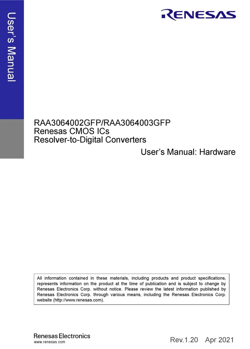
Renesas RAA3064002GFP User manual

Renesas

Renesas RAA3064002GFP User manual

Renesas M16C/62 Installation and operating instructions

Renesas

Renesas M16C/62 Installation and operating instructions

Renesas dialog semiconductor DA913 30 Series User manual

Renesas

Renesas dialog semiconductor DA913 30 Series User manual

Renesas ISL6310EVAL1Z User manual

Renesas

Renesas ISL6310EVAL1Z User manual

Renesas RA6T2 Installation and operating instructions

Renesas

Renesas RA6T2 Installation and operating instructions

Renesas R0E420000CFJ30 User manual

Renesas

Renesas R0E420000CFJ30 User manual

Renesas Single-Chip Microcomputer M32180T2-PTC User manual

Renesas

Renesas Single-Chip Microcomputer M32180T2-PTC User manual

Renesas M3A-ZA53 User manual

Renesas

Renesas M3A-ZA53 User manual

Renesas R0E53036ACFG40 User manual

Renesas

Renesas R0E53036ACFG40 User manual

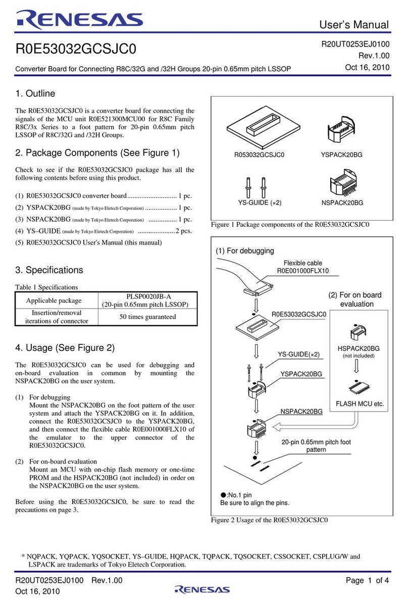
Renesas R0E53032GCSJC0 User manual

Renesas

Renesas R0E53032GCSJC0 User manual

Renesas AB-050-Fx4-MB-L-Q-TCT-V2 User manual

Renesas

Renesas AB-050-Fx4-MB-L-Q-TCT-V2 User manual

Renesas R0E000200ACB10 User manual

Renesas

Renesas R0E000200ACB10 User manual

Renesas RL78/G13 User manual

Renesas

Renesas RL78/G13 User manual

Popular Media Converter manuals by other brands

TR-Electronic CMS582M-4096/4096 IOL DMS 14H7 KRF Assembly instructions

TR-Electronic

TR-Electronic CMS582M-4096/4096 IOL DMS 14H7 KRF Assembly instructions

Korenix JetCon 2301S user manual

Korenix

Korenix JetCon 2301S user manual

StarTech.com ET91000LCOAM manual

StarTech.com

StarTech.com ET91000LCOAM manual

Alesis AI-3 Reference manual

Alesis

Alesis AI-3 Reference manual

Caton Vpro 5100 user guide

Caton

Caton Vpro 5100 user guide

Cypress CSC-5500 Operation manual

Cypress

Cypress CSC-5500 Operation manual

H&B TX-100 Installation and instruction manual

H&B

H&B TX-100 Installation and instruction manual

Bolin Technology D Series user manual

Bolin Technology

Bolin Technology D Series user manual

IFM Electronic Efector 400 RN30 Series Device manual

IFM Electronic

IFM Electronic Efector 400 RN30 Series Device manual

GRASS VALLEY KUDOSPRO ULC2000 user manual

GRASS VALLEY

GRASS VALLEY KUDOSPRO ULC2000 user manual

Linear Technology DC1523A Demo Manual

Linear Technology

Linear Technology DC1523A Demo Manual

Lika ROTAPULS I28 Series quick start guide

Lika

Lika ROTAPULS I28 Series quick start guide

Weidmuller IE-MC-VL Series Hardware installation guide

Weidmuller

Weidmuller IE-MC-VL Series Hardware installation guide

Optical Systems Design OSD2139 Series Operator's manual

Optical Systems Design

Optical Systems Design OSD2139 Series Operator's manual

Tema Telecomunicazioni AD615/S product manual

Tema Telecomunicazioni

Tema Telecomunicazioni AD615/S product manual

KTI Networks KGC-352 Series installation guide

KTI Networks

KTI Networks KGC-352 Series installation guide

Gira 0588 Series operating instructions

Gira

Gira 0588 Series operating instructions

Lika SFA-5000-FD user guide

Lika

Lika SFA-5000-FD user guide

manuals.online logo
manuals.online logoBrands
  • About & Mission
  • Contact us
  • Privacy Policy
  • Terms and Conditions

Copyright 2025 Manuals.Online. All Rights Reserved.

USER’S MANUAL
AN1211
Rev 0.00
Jan 3, 2006
ISL8103EVAL1
Three Phase Buck Converter with Integrated High Current 5-12V Drivers
AN1211 Rev 0.00 Page 1 of 21
Jan 3, 2006
Introduction
The progress in many parts of modern power systems such
as DDR/Chipset core voltage regulators, high current low
voltage DC/DC converters, FPGA/ASIC DC/DC converters
and many other general purpose applications keeps
challenging the power management IC makers to come up
with innovative products and new solutions to meet the
increase in power, reduction in size and increase in the
DC/DC converter’s efficiency targets. The interleaved
multiphase synchronous buck topology proves again to be
the topology of choice for such high current low voltage
applications.
The ISL8103 is a space-saving, cost-effective solution for
such applications. The ISL8103 is a three-phase PWM
control IC with integrated high current MOSFET drivers. The
integration of 5-12V high current MOSFET drivers into the
controller IC marks a departure from the separate PWM
controller and driver configuration of previous multi-phase
product families. By reducing the number of external parts,
this integration allows for a cost and space saving power
management solution.
Output voltage can be programmed using the on-chip DAC
or an external precision reference. A two bit code programs
the DAC reference to one of 4 possible values (0.6V,
0.9V,1.2V and 1.5V). A unity gain, differential amplifier is
provided for remote voltage sensing, compensating for any
potential difference between remote and local grounds. The
output voltage can also be offset through the use of single
external resistor. An optional droop function is also
implemented and can be disabled for applications having
less stringent output voltage variation requirements or
experiencing less severe step loads.
A unique feature of the ISL8103 is the combined use of both
DCR and rDS(ON) current sensing. Load line voltage
positioning and overcurrent protection are accomplished
through continuous inductor DCR current sensing, while
rDS(ON) current sensing is used for accurate channel-current
balance. Using both methods of current sampling utilizes the
best advantages of each technique.
Protection features of this controller IC include a set of
sophisticated overvoltage and overcurrent protection.
Overvoltage results in the converter turning the lower
MOSFETs ON to clamp the rising output voltage and protect
the load. An OVP output is also provided to drive an optional
crowbar device. The overcurrent protection level is set
through a single external resistor. Other protection features
include protection against an open circuit on the remote
sensing inputs. Combined, these features provide advanced
protection for the output load.
The ISL8103EVAL1 evaluation board embodies a 85-90A
regulator solution targeted at supplying power to the
designated load. The physical board design is optimized for
3 phase operation and ships out configured to provide one of
the following four output voltages (0.6V, 0.9V, 1.2V and 1.5V)
depending on choice of the REF1, REF0 combination set by
DIP switch U2, but can be easily modified to provide any
output voltage values in the range of 0.6-2.3V by means of
resistor divider composed of R90 and R81.
For further details on the ISL8103, consult the data sheet [1].
The Intersil multi-phase family controller and driver portfolio
continues to expand with new selections to better fit our
customer needs. Refer to our web site for updated
information: www.intersil.com.
ISL8103EVAL Board Design
The evaluation kit consists of the ISL8103EVAL1 evaluation
board, the ISL8103 datasheet, and this application note. The
evaluation board is optimized for three phase operation
without droop, the nominal output voltage is 1.5V (with DIP
switch U2 set to 11 position) and the maximum output
current is 90A.
The evaluation board provides convenient test points, a DIP
switch for DAC (REF) voltage selection from four possible
values (0.6V, 0.9V, 1.2V and 1.5V), footprint for a resistor
divider for output voltage adjustment up to 2.3V, and an on-
board transient load generator to facilitate the evaluation
process. An on board LED is present to indicate the status of
the PGOOD signal. The board is configured for down
conversion from 5-12V to the REF setting.
The printed circuit board is implemented in 6-layer, 2-ounce
copper. Layout plots and part lists are provided at the end of
this application note for this design.
Quick Start Evaluation
The ISL8103EVAL1 is designed for quick evaluation after
following only a few simple steps. All that is required is two
bench power supplies, Oscilloscope and Load. To begin
evaluating the ISL8103EVAL1 follow the steps below.
1. Before doing anything to the evaluation board, make sure
that the “Enable” switch (S1) is in the Disable position and
the “Transient Load Generator” switch (S2) is in the Load
Off position.
2. Connect a 12V, 15A Lab power supply between J7 and
J8, this power supply provides VIN and PVCC (with
original board configuration).
3. Connect a 5V, 1A Lab power supply between J23 and
GND, this power supply provides VCC bias (and PVCC
bias if the board is configured for 5V PVCC).

AN1211 Rev 0.00 Page 2 of 21
Jan 3, 2006
ISL8103EVAL1
4. Set the “REF Selection” DIP switch (U2) to 11
corresponding to DAC = REF = 1.5V. Figure 1 details the
typical default configuration for U2 when the board is
shipped. In this default setting, the evaluation board is set
for a reference voltage of 1.5V.
5. Connect a load (either resistive or electronic) between
VOUT terminal (J1, J2) and GND terminal (J3, J4).
6. Move the “Enable” switch (S1) to the Enable position
releasing the IC ENLL pin to rise to begin regulation.
After step 6, the ISL8103EVAL1 should be regulating the
output voltage, at the “VOUT+” and “VOUT-” test points
(P20, P21) and J5 to the REF voltage. The “PGOOD
Indicator” LED (D1) should be green to indicate the regulator
is operating correctly.
ISL8103EVAL1 Board Features
Input Power Connections
The ISL8103EVAL1 allows for the use of standard bench
power supplies for powering up the board. Two female-
banana jacks are provided for connection of bench power
supplies. Connect the +5V terminal to P23, +12V terminal to
J7, and the common ground to terminal J8. Voltage
sequencing is not required when powering the evaluation
board.
Once power is applied to the board, the PGOOD LED
indicator will begin to illuminate red. With S1 in the Disable
position, the ENLL pin of the ISL8103 is held low and the
startup sequence is inhibited.
Output Power Connections
The ISL8103EVAL1 output can be exercised using either
resistive or electronic loads. Copper alloy terminal lugs
provide connection points for loading. Tie the positive load
connection to VOUT, terminals J1 and J2, and the negative
to ground, terminals J3 and J4. A shielded scope probe test
point, J5, allows for inspection of the output voltage, VOUT.
REF and VOUT Setup
The REF DIP switch would be preset to 11 (1.500V). Also
1.2V, 0.9V and 0.6V outputs can be selected using different
codes on the DIP switch. If an output voltage different than
the 4 possible REF values is desired, the output resistor
divider composed of R90 (initially 0) and R81 (initially
open) can be used (consult Data sheet and the section
entitled Adjusting the Output Voltage at the end of this
application note for resistor value calculations). Note that the
ISL8103 is usable for output voltages up to 2.3V when the
REF voltage is set to 1.5V. See Table 1 below for the
maximum possible output voltage with different REF setting.
PVCC Power Options
One unique feature of the ISL8103 is the variable gate drive
bias for the integrated drivers. The gate drive voltage for the
internal drivers can be any voltage from +5V to +12V by
simply connecting the desired voltage to the PVCC pin of the
controller. To accommodate the flexibility of the drivers, the
ISL8103EVAL1 has been designed to support a multitude of
options for the PVCC voltage.
Switching between the different PVCC voltages available on
the evaluation board is as simple as populating and
depopulating certain resistors. The eval board has three on
board voltages available: +5V, +12V, and +8V (from an
onboard linear regulator). Refer to Table 2 for what resistors
to populate for each voltage option.
Enabling the Controller
In order to enable the controller, the board must be powered,
a REF (DAC) code must be set, and the PVCC and VCC
voltages must be set. If these steps have been properly
followed, the regulator is enabled by toggling the “ENABLE”
switch (S1) to the Enable position, which allows the voltage
on the ENLL pin of the ISL8103 to rise above the ENLL
threshold of 0.66V and the controller will begin its digital soft
start sequence. The output voltage ramps up to the
programmed setting, at which time the PGOOD indicator will
switch from red to green.
On-Board Load Transient Generator
Most bench-top electronic loads are not capable of
producing the current slew rates required to emulate most
modern loads. For this reason, a discrete transient load
FIGURE 1. TYPICAL U2 DEFAULT SETTING 11 (1.500V)
REF0
REF1
1
2
ON
1
0
Logic
TABLE 1. MAXIMUM OUTPUT VOLTAGE WITH DIFFERENT
REF SETTING WITH THE USE OF A RESISTOR
DIVIDER ON VSEN
REF1 REF0 REF=DAC VOUT MAX
0 0 0.6V 1.4V
0 1 0.9V 1.7V
1 0 1.2V 2V
1 1 1.5V 2.3V
TABLE 2. GATE DRIVE VOLTAGE OPTIONS AND RESISTOR
SETTINGS
UGATE
VOLTAGE
LGATE
VOLTAGE R48 R68 R71 R72
12.0V 12.0V OPEN OPEN OPEN 0
8.0V 8.0V OPEN OPEN 0OPEN
5.0V 5.0V 0OPEN OPEN OPEN
12.0V 5.0V 00OPEN OPEN
AN1211 Rev 0.00 Page 3 of 21
Jan 3, 2006
ISL8103EVAL1
generator is provided on the evaluation board, see Figure 2.
The generator produces a load pulse of 550s in duration
with a period of 70ms. The pulse magnitude is approximately
30A with rise and fall slew rates of approximately 50A/s as
configured. The short load current pulse and long duty cycle
is required to limit the power dissipation in the load resistors
(R38-R42) and MOSFETs (Q20, Q21). To engage the load
generator simply place switch S2, in the “OFF” position.
If the DAC code is changed from 11(1.500V), the transient
generator dynamics must be adjusted relative to the new
output voltage level. Place a scope probe in J10 to measure
the voltage across the load resistors and the dV/dt across
them as well. Adjust the load resistors, R38-R40, to achieve
the correct load current level. Change resistors R34-R37 to
increase or decrease the dV/dt as required to match the
desired dI/dt profile.
Inductor DCR Static Current Sense Points
A unique feature of the ISL8103EVAL1 is the ability to
measure the voltage drop across the DCR of each channel’s
inductor by multimeter. This is accomplished with the use of
a capacitor and resistor series circuit which is placed in
parallel across each inductor as illustrated in Figure 3. When
current, IL, flows through the inductor, the voltage drop
developed across the DCR will be sensed by the R-C circuit,
and an equivalent voltage will be developed across the
capacitor C.
.
In order to not affect the rest of the regulator, the time
constant of this R-C circuit is very large, so it can only be
used to measure static current, and not transient currents. To
calculate the current through each inductor measure the
voltage across the “DCR SENSE” points on the
ISL8103EVAL1 and then divide that number by the DCR of
the inductor. This should give you an accurate reading of the
current through each channel during static loads.
Modifying the ISL8103EVAL1 Design
Current Balance Resistors
The ISL8103 uses lower MOSFET rDS(ON) current sensing to
measure the current through each channel and balance them
accordingly. If the lower MOSFETs on the ISL8103EVAL1 are
changed, the current balance resistors, R18-R20, should also
be changed to adjust for the change in rDS(ON). Refer to page
19 in the ISL8103 datasheet to choose new current sense
resistors. R18 adjusts the current in channel 1, R19 adjusts
the currents in channel 3 and R20 adjusts the currents in
channel 2. These resistors can also be changed to adjust for
any current imbalance due to layout, which is also explained
on page 19 of the ISL8103 datasheet.
Load Line (Droop) Regulation
The ISL8103 has an optional Droop function, the
ISL8103EVAL1 board design is optimized for no Droop case.
For Droop option selection follow Table 3.
If Droop is implemented, the compensation network will need to
be recalculated for optimal loop response and stability.
To create an output voltage change proportional to the total
current in all the active channels (droop), the ISL8103 uses an
inductor DCR sensing R-C network. This network, shown in
Figure 4, is designed not only to precisely control the load line
of the regulator, but also to thermally compensate for any
changes in DCR that may skew the load line as a result of
increases in temperature.
HIP2100
VSS
VDD
L I
H I
HB
LO
HS
HO
R33
402
1µF
C55
Q19
R30
46.4k
VCC12
2N7002 22µF
C57
ON
OFF
R35
562
R34
249
R37
562k
R36
249
VOUT
Q20 Q21
R38
0.05
R40
OPEN
R39
OPEN
S3
S4
SUD50N03 SUD50N03
BAV99LT1
BAV99LT1
FIGURE 2. LOAD TRANSIENT GENERATOR
U2
S2
R41
OPEN
R42
OPEN J10
VLOAD
TABLE 3. SELECTION OF DROOP OPTION
DROOP R86 R85
Disabled (Droop
connected to IREF)
0OPEN
Enabled (Droop
connected to ICOMP)
OPEN 0
RC
FIGURE 3. DCR STATIC CURRENT SENSE CIRCUIT
VIN
ISL8103
DCR
L
INDUCTOR
VOUT
COUT
IL
+-
DCR
SENSE
AN1211 Rev 0.00 Page 4 of 21
Jan 3, 2006
ISL8103EVAL1
This sensing technique works off the principle that if the R-C
time constant of C7 * Rcomp (Rcomp = R14) is equal to the
L/DCR time constant of the inductor, the load line impedance
will be equal to Rcomp*DCR/R15 (R15, R16 and R17 are
equal).
If the load line impedance needs to be changed, all that is
required is adjusting the values of R15-R17 as explained on
page 20 of the ISL8103 datasheet. If the Inductor is changed
though, the resistance of time constant matching network
will need to be changed. The NTC resistor network must first
be adjusted so that the new L/DCR time constant is precisely
matched. Refer to page 19 and 20 of the ISL8103 datasheet
to design the entire R-C sense network.
An Optional NTC resistor network consisting of 3 resistors
(R9, R10, and R14) and a single NTC thermistor (R12),
which is placed close the output inductors. This network is
designed to compensate for any change in DCR that occurs
due to temperature when the Droop option is used and a
tight load-line regulation is required, and keep the time
constant of the R-C network equal to that of the inductor
L/DCR time constant.
Overcurrent Protection Level
The ISL8103 utilizes a single resistor to set the maximum
current level for the IC’s overcurrent protection circuitry.
Please refer to page 17 of the ISL8103 datasheet, and
adjust resistor R11 accordingly to set the desired overcurrent
trip level.
Output Voltage Offset
The ISL8103 allows a designer to accurately offset the
output voltage both negatively and positively. All that is
required is a single resistor between the OFS and VCC pins,
or the OFS pin and GND. The ISL8103EVAL1 has both of
these resistor options available on the board. To positively
offset the output voltage populate resistor R5. To negatively
offset the output voltage populate resistor R7. Please refer to
page 13 of the ISL8103 datasheet to accurately calculate
these resistor values.
Switching Frequency
The switching frequency of the ISL8103EVAL1 board is set
to an optimal value of 325kHz giving the best efficiency and
performance for the given design with R13 = 75k.
However, the switching frequency can be adjusted anywhere
from 80kHz to 1.5MHz per phase. In practice many factors
affect the choice of switching frequency among which are
efficiency, and gate drive losses (which depend on the
MOSFET choice and Gate Driver Voltage). Since the
ISL8103 has integrated MOSFET drivers, the driver losses
must be taken into account when the switching frequency is
chosen. To change the switching frequency refer to page 24
of the ISL8103 datasheet and adjust the value of frequency
set resistor, R13, accordingly.
MOSFET Gate Drive Voltage (PVCC)
The gate drive bias voltage of the integrated drivers in the
ISL8103 can be any voltage between +5V and +12V. This
bias voltage is set by connecting the desired voltage to the
PVCC pins of the IC. Please refer to the PVCC Power
Options section to set the desired gate drive voltage.
Number of Active Phases
The ISL8103 has the option of 1, 2 or 2-phase operation.
The ISL8103EVAL1 is designed to change the number of
active phases by simply populating or depopulating few
resistors, R62 - R65. Refer to Table 4 for which resistors to
populate for 1, 2 or 3-phase operation.
ISL8103 Performance
Soft-Start Interval
The typical start-up waveforms for the ISL8103EVAL1 are
shown in Figure 5. The waveforms represented in this image
show the soft-start sequence of the regulator with the DAC
set to 1.50V. Before the soft-start interval begins, VCC and
PVCC are above POR and the DAC inputs are set to logic
11. With these two conditions met, throwing the ENABLE
FIGURE 4. DCR SENSING CONFIGURATION WITH
OPTIONAL FOOTPRINTS FOR NTC LOAD-LINE
COMPENSATION
ICOMP
R17
L2
VOUT
L4
PHASE1
PHASE3
R15
RCOMP
C7
ISUM
IREF
ISL8103
IOUT
R9
R12
R14
R10
OPTIONAL NTC RESISTOR NETWORK
10nF
* R15-R17 ARE EQUAL
0
DNP
DNP
L3
R16
PHASE2
TABLE 4. SETTINGS FOR NUMBER OF ACTIVE PHASES
# OF ACTIVE
PHASES R62 R63 R64 R65
300OPEN OPEN
2 OPEN 00OPEN
1 OPEN OPEN 00
AN1211 Rev 0.00 Page 5 of 21
Jan 3, 2006
ISL8103EVAL1
switch into the Enable position causes the voltage on the
ENLL pin to rise above the ISL8103’s enable threshold,
beginning the soft-start sequence. For a delay time of
0.85ms, VOUT does not move due to the manner in which
soft-start is implemented within the controller. After this delay
(which is approximately equal to 240 switching cycles),
VOUT begins to ramp linearly toward the DAC voltage. With
the converter running at 325kHz, this ramp takes
approximately 5.2ms, during which time the input current,
ICC12, also ramps slowly due to the controlled building of
the output voltage.
Once VOUT reaches the DAC set point, the internal pull-
down on the PGOOD pin is released. This allows a resistor
from PGOOD to VCC to pull PGOOD high and the PGOOD
LED indicator changes from red to green.
Special consideration is given to start-up into a pre-charged
output (where the output is not 0V at the time the SS cycle is
initiated). Under such circumstances, the ISL8103 keeps off
both sets of output MOSFETs until the internal ramp starts to
exceed the output voltage sensed at the FB pin. This special
scenario is detailed in Figure 6. The circuit is enabled at time
T0. As the internal ramp exceeds the magnitude of the
output voltage at time T1, the MOSFETs drivers are enabled
and the output voltage ramps up in a seamless fashion from
the pre-existent level to the DAC-set level, reached at time
T2.
A second scenario can be encountered with a pre-charged
output: output being pre-charged above the DAC-set point,
as shown in Figure 7. In this situation, the ISL8103 behaves
in a way similar to that of Figure 6, keeping the MOSFETs off
until the end of the SS ramp. However, once the end of the
ramp has been reached, at time T1, the output drivers are
enabled for operation, and the output is quickly drained
down to set-point level.
An OV condition during start-up will take precedence over
this normal start-up behavior, but will allow reversal back to
normal behavior as soon as the condition is removed or
brought under control.
FIGURE 5. SOFT-START INTERVAL WAVEFORMS
0V
0A
0V
0A
VOUT
ICORE,
ICC12
ENLL
1ms/DIV
2.0V/DIV 10.0A/DIV 50.0A/DIV 1.0V/DIV
FIGURE 6. ISL8103EVAL1 START-UP INTO A PARTIALLY
CHARGED OUTPUT (VDAC =1.200V)
GND>
GND>
500mV/DIV 20.00V/DIV
2.00V/DIV 20.00V/DIV
ENLL
T0 T1 T2
GND>
GND>
UGATE1
UGATE2
VOUT
1ms/DIV
FIGURE 7. ISL8103EVAL1 START-UP INTO AN
OVERCHARGED OUTPUT (VDAC = 1.200V)
1ms/DIV
GND>
GND>
500mV/DIV 20.00V/DIV
2.00V/DIV 20.00V/DIV
VOUT
ENLL
UGATE1
UGATE2
GND>
GND>
T0 T1
AN1211 Rev 0.00 Page 6 of 21
Jan 3, 2006
ISL8103EVAL1
Transient Response
The ISL8103EVAL1 is designed without droop for a
maximum output load current of 90A. The Load step is
approximately 30A and the output voltage variation during
the transient is kept below 100mV peak to peak. This load
step have a maximum slew rate of approximately 50A/s on
both the rising and falling edges. The on-board load
transient generator is designed to provide the specified load
step, different load steps and current slew rates can be
accommodated with the on Board Transient Load Generator.
The rising edge transient response of the ISL8103EVAL1, is
shown in Figure 8. In order to obtain the load current
waveform shown, the bench-top load is turned off, while the
on-board transient generator is pulsing a 30A step for 550s.
When the load step occurs, the output capacitors provide the
initial output current, causing VOUT to drop suddenly due to
the ESR and ESL voltage drops in the capacitors. The
controller immediately responds to this drop by increasing
the PWM duty cycles to as much as 66%. The duty cycles
then decrease to stabilize VOUT.
At the end of the 550s load pulse, the load current returns
to 0A. The transient response to this falling edge of the load
is shown in Figure 9. When the falling load step occurs, the
output capacitors must absorb the inductor current which
can not fall at the same rate of the load step. This causes
VOUT to rise suddenly due to the ESR and ESL voltage
drops in the capacitors. The controller immediately responds
to this rise by decreasing the PWM duty cycles to zero, and
then increasing them accordingly to regulate VCORE to the
programmed 1.5V level.
Figure 10 shows both the rising and falling edges.
Overcurrent Protection
The ISL8103 is designed to stop all regulation and protect
the sensitive Load if an overcurrent event occurs. This is
done by continuously monitoring the total output current and
comparing it to an overcurrent trip level set by the OCSET
resistor, R11. If the output current ever exceeds the trip level
as shown in Figure 11 (at time T1), the ISL8103 immediately
turns the upper and lower MOSFETs off, causing VOUT to
fall to 0V. The controller holds the UGATE and LGATE
signals in this state for a period of 4096 switching cycles,
which at 325kHz is 13.65ms. The controller then re-initializes
the soft-start cycle (at time T2). If the load that caused the
overcurrent trip remains, another overcurrent trip will occur
before the soft-start cycle completes. The controller will
continue to try to cycle soft-start indefinitely until the load
current is reduced, or the controller is disabled. This
operation is shown in Figure 11.
FIGURE 8. ISL8103EVAL1 RISING EDGE TRANSIENT LOAD
RESPONSE
20mV/DIV
1.0V/DIV
20µs/DIV
VOUT
V(ILOAD)
GND>
FIGURE 9. ISL8103EVAL1 FALLING EDGE TRANSIENT
RESPONSE
20mV/DIV
1.0V/DIV
20µs/DIV
VOUT
V(ILOAD)
GND>
FIGURE 10. ISL8103EVAL1 TRANSIENT RESPONSE
20mV/DIV
1.0V/DIV
100µs/DIV
VOUT
V(ILOAD)
GND>
AN1211 Rev 0.00 Page 7 of 21
Jan 3, 2006
ISL8103EVAL1
Pre-POR Overvoltage Protection
Prior to PVCC and VCC exceeding their POR levels, the
ISL8103 is designed to protect the load from any overvoltage
events that may occur (such an overvoltage may occur if for
example one of the upper MOSFETs was shorted at
assembly due to manufacturing defects). This is
accomplished by means of an internal 10k resistor tied
from PHASE to LGATE, which turns on the lower MOSFET
to control the output voltage until the input power supply
current limits itself and cuts off. In Figure 12, an artificial pre-
POR overvoltage event has been created by shorting the
positive 12V input plane to the PHASE plane. This same
12V input is connected to PVCC pins of the ISL8103.
Figure 12 illustrates how the controller protects the load from
a high output voltage spike, when the 12V input turns on, by
tying LGATE to PHASE.
Overvoltage Protection
To protect from an overvoltage event during normal
operation, the ISL8103 continually monitors the output
voltage. If the output voltage exceeds a specific limit (set
internally), the controller commands the LGATE signals high,
turning on the lower MOSFETs to keep the output voltage
below a level that might cause damage to the Load. As
shown in the overvoltage event in Figure 12, turning on the
lower MOSFETs not only keeps the output voltage from
rising, it also sinks a large amount of current, causing the
input voltage to the power stage to drop. If this causes the
input power supply voltage to fall below the POR level of the
ISL8103, as seen at the end of the waveform in Figure 13,
the controller responds by using the pre-POR overvoltage
protection explained in the previous section. This allows the
ISL8103 to always keep the output load safe from high
voltage spikes during an entire overvoltage event.
Efficiency
The efficiency of the ISL8103EVAL1 board, loaded from 0A
to 90A, at both PVCC = 5V and 12V are plotted in Figure 14
for VOUT = 1.5V. Measurements were performed at room
temperature and taken at thermal equilibrium with an air flow
of 200LFM. The efficiency peaks just below 89% at 50A for
the PVCC = 12V case and then levels off steadily to
approximately 86.5% at 90A, while for the PVCC = 5V,
efficiency peaks at around 90% at 25A and then falls down
to approximately 85% at 90A.
FIGURE 11. ISL8103EVAL1 OVERCURRENT PROTECTION
GND>
500mV/DIV 5.00V/DIV
1.00V/DIV 20.00V/DIV
5ms/DIV
VOUT
UGATE1
COMP
PGOOD
GND>
GND>
GND>
T1 T2
FIGURE 12. ISL8103EVAL1 PRE-POR OUTPUT OVER-
VOLTAGE PROTECTION (START-UP WITH
SHORTED UPPER FET)
GND>
1.0V/DIV
2.0V/DIV 1.0V/DIV
10ms/DIV
VOUT
LGATE2
Vin = PVCC
GND>
GND>
FIGURE 13. ISL8103EVAL1 PRE-POR OVERVOLTAGE
PROTECTION
GND>
2.00V/DIV
5.00V/DIV
500µs/DIV
VOUT
LGATE2
Vin = PVCC
GND>
GND>
10.00V/DIV
AN1211 Rev 0.00 Page 8 of 21
Jan 3, 2006
ISL8103EVAL1
The efficiency for VOUT = 1.8V is plotted in Figure 15. The
efficiency peaks around 90% at 50A for the PVCC = 12V case
and then levels off steadily to approximately 88% at 90A,
while for the PVCC = 5V, efficiency peaks at around 91% at
30A and then falls down to approximately 87% at 90A. The
use of stronger air flow could improve the efficiency across
the load range and keeps the components cooler leading to
better reliability and longer component lives.
Modifications
Adjusting the Output Voltage
The output voltage can be adjusted by changing the 2 bit
inputs (REF1, REF0) of internal DAC (externally connected
with a resistor to REF). Please consult the data sheet for the
available voltage ranges and the required settings.
The offset pin (OFS) allows for small-range (less than
100mV), positive or negative, offsetting of the output voltage.
The board is shipped with R90 equal to 0and R82 is not
populated to provide an output voltage equal to the internal
DAC setting. Should an output voltage setting outside the
normal range provided via the internal DAC be required, a
separate resistor divider connected from the load output
terminals to VSEN pin as shown in Figure 16 is needed.
Use the following relationships to calculate the value of the
resistors based on the known parameters.
Choose a value of VREF that meets the following condition
Choose a value for RL (for example 300)
Calculate the value of the resistor RH
Example:
VOUT=2.1V
70
72
74
76
78
80
82
84
86
88
90
92
0 5 10 15 20 25 30 35 40 45 50 55 60 65 70 75 80 85 90
LOAD CURRENT ( A )
EFFICIENCY ( % )
FIGURE 14. EFFICIENCY vs LOAD CURRENT
VOUT = 1.5V
Fsw = 325kHz
PVCC = 12V
PVCC = 5V
70
72
74
76
78
80
82
84
86
88
90
92
0 5 10 15 20 25 30 35 40 45 50 55 60 65 70 75 80 85 90
LOAD CURRENT ( A )
EFFICIENCY ( % )
FIGURE 15. EFFICIENCY vs LOAD CURRENT
VOUT = 1.8V
Fsw = 325kHz
PVCC = 12V
PVCC = 5V
FB
COMP
ISL8103
4
5
C1
R1
C2
R4
C4
R3
FIGURE 16. ADJUSTING VOUT OUTSIDE THE REF (DAC)
RANGE
6
VDIFF
RH = R90
RL = R81
VOUT+
VOUT-
78
VSEN
RGND
RLRH
+500
RL300=
Choose
VREF VOUT 0.8V–
RH
RLVOUT REF–
REF
-----------------------------------------------------
=
VREF 2.1V 0.8V–1.3V
VREF 1.5V=
RL300=
RH
3002.1V 1.5V–
1.5V
--------------------------------------------------------120==
AN1211 Rev 0.00 Page 9 of 21
Jan 3, 2006
ISL8103EVAL1
Down-Converting From a Different Input Voltage
The ISL8103EVAL1 is powered from bench supplies, the
input labelled ‘+12V’ can be adjusted down as desired. If
experimenting with a lower voltage, be mindful of a few
aspects:
• The duty cycle of the controller is limited to 66%; the
circuit will not be capable of properly regulating the output
voltage should the input be reduced to a level low enough
to induce duty cycle saturation
• As the evaluation board (as shipped) was not optimized
for high duty cycle operation, closely monitor the board
temperatures and increase the output current only as
allowed by the board thermal behaviour
• The reduced input voltage will decrease the amount of
loop gain the modulator provides in the feedback loop, as
a result, expect a more sluggish transient response when
operating the board at reduced down-conversion voltage
• The Evaluation Board (as shipped) have the +12V
connected as the input to be down-converted and
provides gate drive bias (PVCC). Since PVCC can
assume any value between +5 and +12V, the Input can be
reduced only to 5V. If a lower input voltage is desired, the
PVCC voltage should be provided by a separate supply
whose value does not drop below +5V. The VCC bias
supply can be used in this case (Consult the section
entitled PVCC Power Options for more details on how
this can be accomplished)
Summary
The ISL8103EVAL1 evaluation board showcases a highly
integrated approach to providing control in a wide variety of
applications. The sophisticated feature set and high-current
MOSFET drivers of the ISL8103 yield a highly efficient
power conversion solution with a reduced number of
external components in a compact footprint. The following
pages provide a board schematic, bill of materials and layout
drawings to support implementation of this solution.
References
Intersil documents are available on the web at
www.intersil.com.
[1] ISL8103 Data Sheet, Intersil Corporation, File No.
FN9246.
AN1211 Rev 0.00 Page 10 of 21
Jan 3, 2006
ISL8103EVAL1
IISL8103EVAL1 Schematic