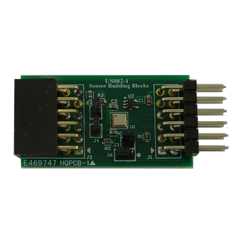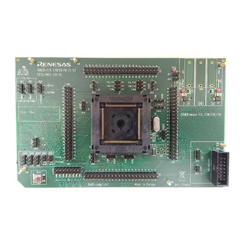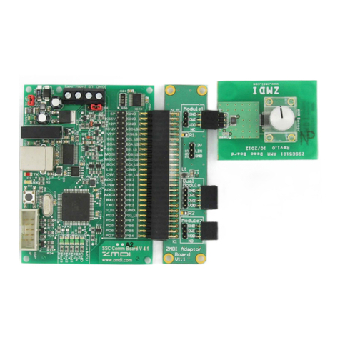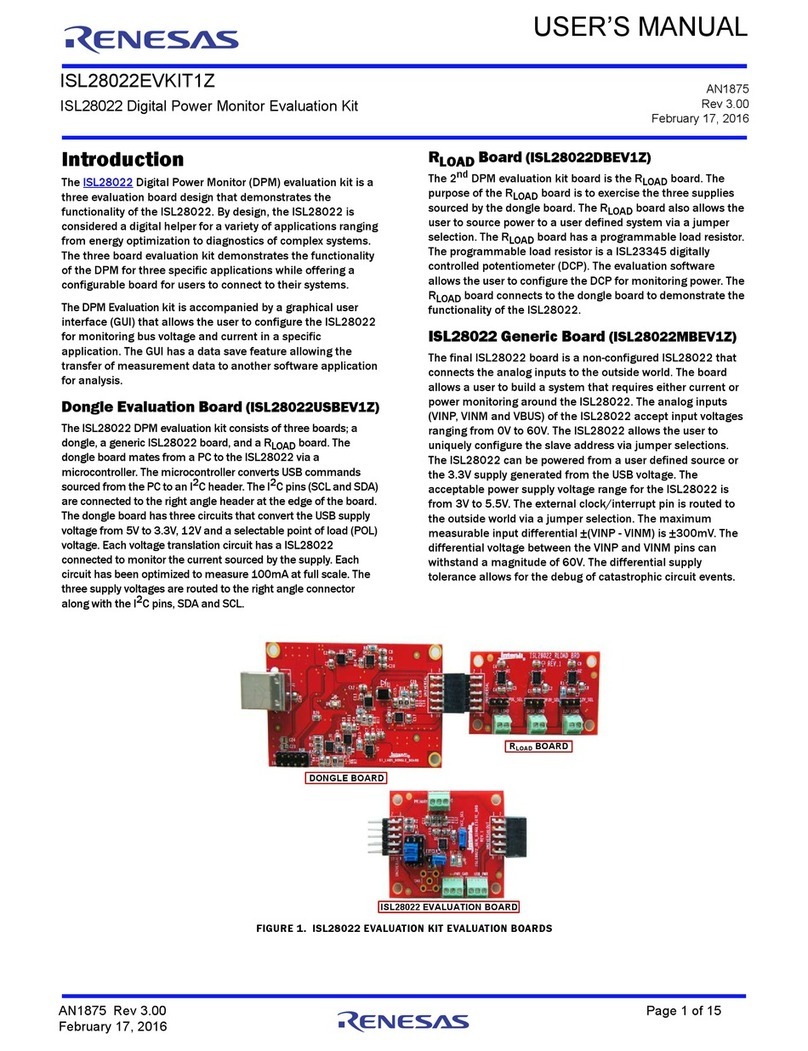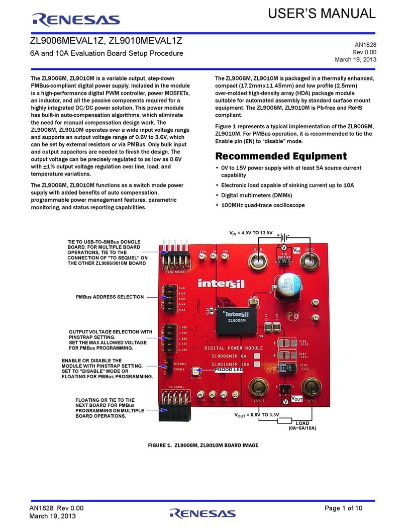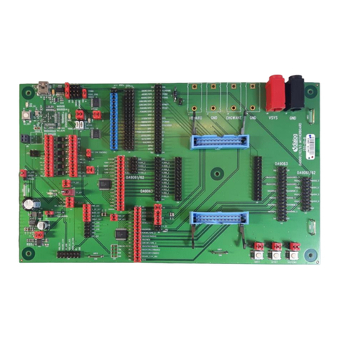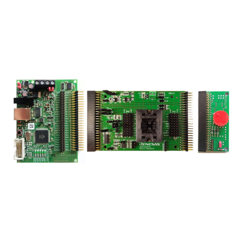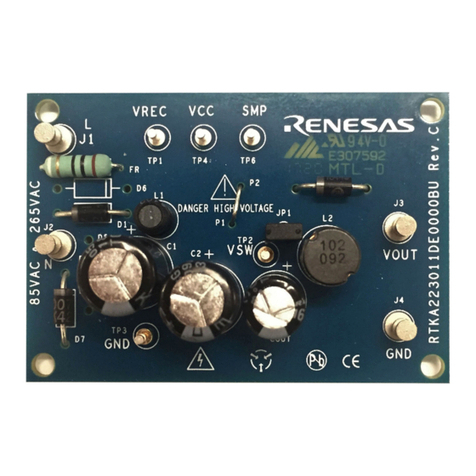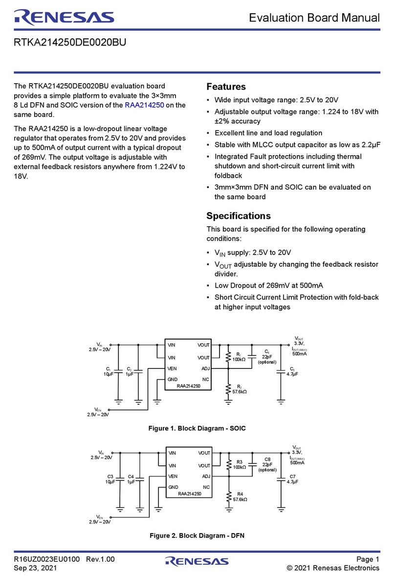
ISL85410EVAL1Z, ISL854102EVAL1Z, ISL85418EVAL1Z
Evaluation Boards User Guide
AN1905 Rev.4.00 Page 2 of 11
Oct 18, 2016
Recommended Equipment
The following materials are recommended to perform testing:
• 0V to 50V power supply with at least 2A source current
capability
• Electronic loads capable of sinking current up to 2A
• Digital Multimeters (DMMs)
• 100MHz quad-trace oscilloscope
• Signal generator
Quick Setup Guide
1. Ensure that the circuit is correctly connected to the supply and
loads prior to applying any power.
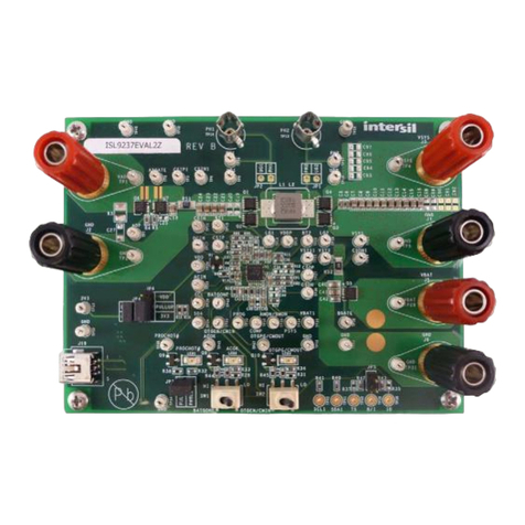
2. Connect the bias supply to VIN, the plus terminal to VIN (P4),
and the negative return to GND (P5).
3. Verify that the position is ON for S1.
4. Turn on the power supply.
5. Verify the output voltage is 3.3V for VOUT.
Evaluating the Other Output Voltage
The ISL85410EVAL1Z, ISL854102EVAL1Z and ISL85418EVAL1Z
board outputs are preset to 3.3V; however, output voltages can
be adjusted from 0.6V to 15V. The output voltage programming
resistor, R2, will depend on the desired output voltage of the
regulator and the value of the feedback resistor R1, as shown in
Equation 1.
If the output voltage desired is 0.6V, then R1is shorted. Please
note that if VOUT is less than 1.8V, the switching frequency and
compensation must be changed for 300kHz operation due to
minimum on-time limitation. Please refer to datasheets
ISL85410, ISL854102, and ISL85418 for further information.
Table 1 shows the component selection that should be used for
the respective VOUT.
Frequency Control
The ISL85410, ISL854102, and ISL85418 have an FS pin that
controls the frequency of operation. Programmable frequency
allows for optimization between efficiency and external
component size. It also allows low frequency operation for low
VOUTs when minimum on-time would limit the operation
otherwise. Default switching frequency is 500kHz when FS is tied
to VCC (R10 = 0). By removing R10, the switching frequency could
be changed from 300kHz (R12 = 340k) to 2MHz (R12 = 32.4k).
Please refer to datasheets ISL85410, ISL854102, and ISL85418
for calculating the value of R10. Do not leave this pin floating.
Disabling/Enabling Function
The ISL85410, ISL85418 evaluation boards contain an S1 switch
that enables or disables the part, thus allowing low quiescent
current state. Table 2 details this function.
SYNC Control
The ISL85410, ISL85418 evaluation boards have a SYNC pin that
allows external synchronization frequency to be applied. Default
board configuration has R6 = 200k to VCC, which defaults to
PWM operation mode and also to the preselected switching
frequency set by R12 (see datasheets and previous section
“Frequency Control”for details). If this pin is tied to GND the IC
will operate in PFM mode. The S2 switch allows forced PFM or
PWM modes.
Soft-Start/COMP Control
R15 selects between internal (R15 = 0) and external soft-start.
R11 selects between internal (R11 = 0) and external
compensation. For applications where repetitive restarts of the
IC are required, it is recommended to add a 350kΩresistor in
parallel to CSS in order to allow its fast discharge. Please refer to
the pin description table of the ISL85410, ISL854102, and
ISL85418 datasheets.
TABLE 1. EXTERNAL COMPONENT SELECTION
VOUT
(V)
L1
(µH)
C5 +C6
(µF)
R1
(kΩ)
R2
(kΩ)
C4
(pF)
R12
(kΩ)
R3
(kΩ)
C7
(pF)
12 22 2x22 90.9 4.75 22 115 150 470
5 22 47+22 90.9 12.4 27 DNP
(Note 1)
100 470
3.3 22 47+22 90.9 20 27 DNP
(Note 1)
100 470
2.5 22 47+22 90.9 28.7 27 DNP
(Note 1)
100 470
1.8 12 47+22 90.9 45.5 27 DNP
(Note 1)
70 470
NOTE:
1. Connect FS to VCC.
R2R1
0.6
VOUT 0.6–
------------------------------
=(EQ. 1)
TABLE 2. SWITCH SETTINGS
S1 ON/OFF CONTROL
ON Enable VOUT
OFF Disable VOUT

