Richardson RFPD RadioCarbon RFPD-RC-4450-50 User manual

RFPD-RC-4450-50 4.4-5 GHz, 2W Linear
Front-End Design Accelerator
Quick Start Guide

RFPD-RC-4450-50 Design Accelerator –Quick Start Guide
1

RFPD-RC-4450-50 Design Accelerator –Quick Start Guide
2
1Table of Contents
2 Introduction - About This Document...........................................................................................................3
3 RFPD-RC-4450-50 Module –Standalone Mode ..........................................................................................4
4 RF Bench Setup –Standalone Transmit .......................................................................................................5
5 Hardware Setup –Standalone Transmit......................................................................................................6
5.1 DC Power Supply Connection......................................................................................................................6
5.2 Digital/Control - USB/TTL Cable Connection ...............................................................................................7
5.3 RF Port Connections ....................................................................................................................................7
6 Software Setup –Standalone Transmit.......................................................................................................8
6.1 Launch RadioCarbon Software App.............................................................................................................8
oOpen the App for the RFPD-RC-4450-50 Frontend module by clicking on the icon ( .................................8
6.2 Biasing the RadioCarbon PA ......................................................................................................................10
6.3 Turn RF signal ON ......................................................................................................................................12
6.4 Transmitter Turn OFF Sequence................................................................................................................12
7 Hardware Setup –Receiver Operation......................................................................................................13
7.1 Software Setup –Receiver Operation .......................................................................................................14
7.2 Turn Receiver OFF......................................................................................................................................15
List of Figures
Figure 1: RFPD-RC-4450-50 Simplified Block Diagram............................................................................................ 3
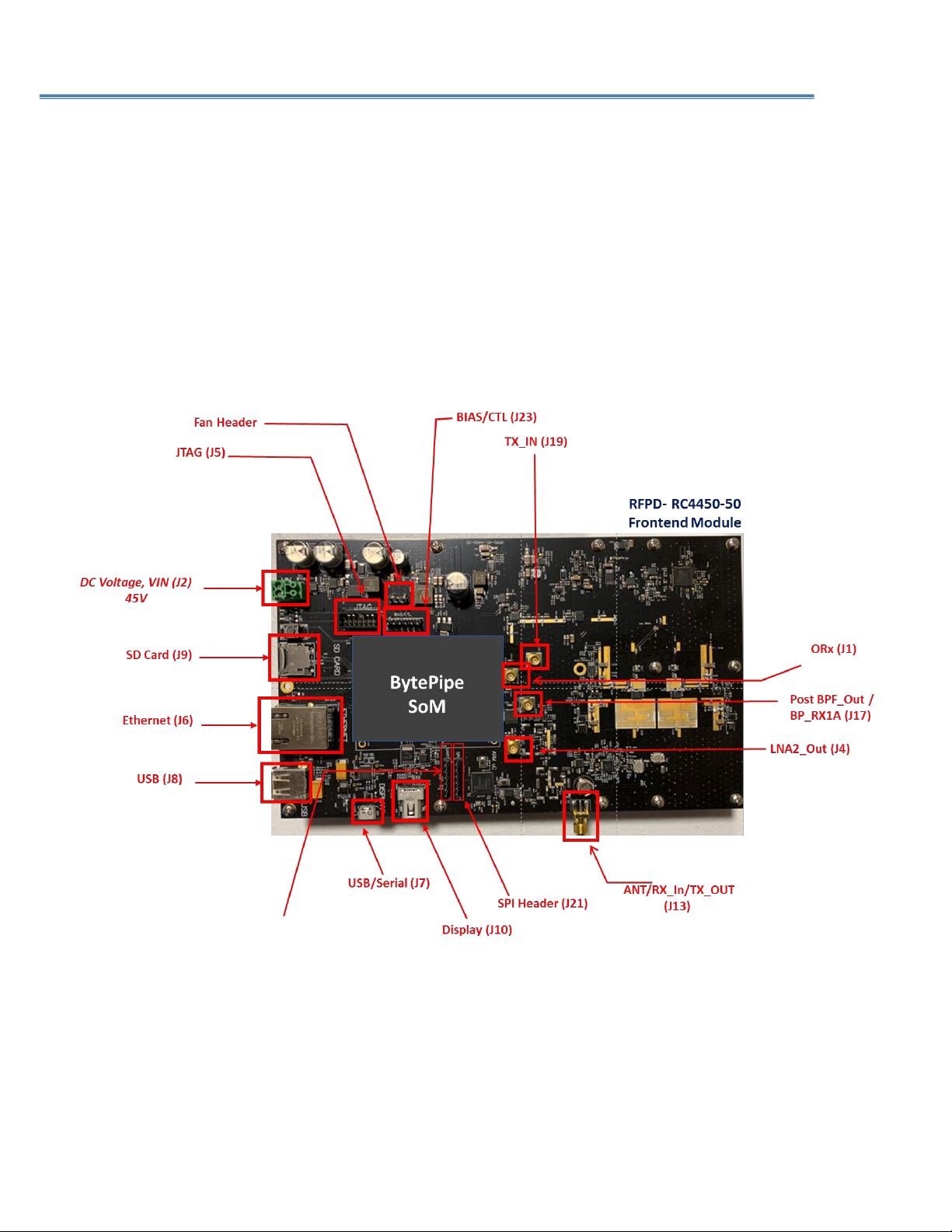
Figure 2: RFPD-RC-4450-50 RF Frontend Module with Input/Output Interfaces. ................................................. 4
Figure 3: Suggested Configuration for RFPD-RC-4450-50 Transmit Evaluation. .................................................... 5
Figure 4: DC Voltage VIN connection...................................................................................................................... 6
Figure 5: USB to TTL/UART cable............................................................................................................................ 7
Figure 6: Serial cable connection to J15 ................................................................................................................. 7
Figure 7: Icon........................................................................................................................................................... 8
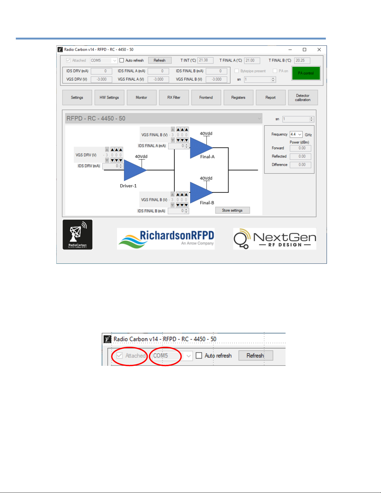
Figure 8: Main Screen ............................................................................................................................................. 9
Figure 9: COM port Highlighted.............................................................................................................................. 9
Figure 10: Auto Refresh Box Checked................................................................................................................... 10
Figure 11: Main Screen –Setting PA Bias ............................................................................................................. 10
Figure 12: PA Bias “Quick View” ........................................................................................................................... 11
RFPD-RC-4450-50_ADRV9002 EVAL PLATFORM_QSG_9/22/2021

RFPD-RC-4450-50 Design Accelerator –Quick Start Guide
3
Figure 13: PA Power-Down................................................................................................................................... 12
Figure 14: Idq Verification..................................................................................................................................... 13
Figure 15: Receiver Test bench Setup................................................................................................................... 14
Figure 16: Main Window - Frontend..................................................................................................................... 15
List of Tables
Table 1: PA Bias Settings for Class AB operation.................................................................................................. 11
2Introduction - About This Document
This document serves as a Quick Start Guide to assist users in powering up and performing Bench level
testing/evaluation of the “RadioCarbon” RFPD-RC-4450-50 RF Frontend module from Richardson RFPD in
standalone mode. The RFPD-RC-4450-50 Frontend module serves as a “Design Accelerator” platform targeting
RF Frontend communications applications in the 4.4 to 5 GHz frequency band. Figure 1 shows a simplified block
diagram.
RFPD-RC-4450-50
Pre-Driver
30dB Coupler
LNA with Bypass
MHz
50Ω
A
Circulator
LNA
1
2
Σ
Forward
Pi
10 dB
SPDT Switch
RMS Power Detect
In 90°
0°Iso
Hybrid In90°
0° Iso
Hybrid
50Ω
A
50Ω
A
A
50Ω
50Ω
A
##
Ω##
nF
20dB Coupler
Forward Detect Forward
Reverse Detect
VSWR Detect
Driver
J13
Antenna
TX IN
J19
Tunable Band
Pass Filter
Pi
15 dB J1 MCX
Aux RX OutSplitter
25W PSAT HPA
25W PSAT HPA
3dB Hybrid Coupler
3dB Hybrid Coupler
RX Out
J17
Microcontroller
Power Amplifier
Current Controller
SoM Connector
JTAG/UART
ETHERNET
USB Micro-B
SD CARD
DISPLAY PORT
USB A 2.0
VIN
45 V
DC/DC 40V
J2
Figure 1: RFPD-RC-4450-50 Simplified Block Diagram

RFPD-RC-4450-50 Design Accelerator –Quick Start Guide
4
3RFPD-RC-4450-50 Module –Standalone Mode
In Standalone mode, the input RF Transmitter signal to the RFPD-RC-4450-50 module is sourced from a Signal
Generator and is applied at the 50 Ohm TX_IN Port (J19) as shown in the picture in Figure 2 below which shows
the actual RFPD-RC-4450-50 module with the various input/Output connections. Please note that Port J19 is a
MCX connector and there is a MCX to SMA adaptor included in the kit. The RF Output signal is delivered to the
50 Ohm RF_OUT port (J13), padded down with a 50 Ohm coaxial attenuator and measured with a
Signal/Spectrum Analyzer and Power Meter.
Figure 2: RFPD-RC-4450-50 RF Frontend Module with Input/Output Interfaces.

RFPD-RC-4450-50 Design Accelerator –Quick Start Guide
5
DC Power to the module is provided via an external DC Power Supply and is applied at the DC Voltage (VIN) port
J2 ( Figure 2 above). This power supply input feeds a series of on-board switching regulators that generate the
additional voltages required for the individual circuits used (including MCU and PA Bias Controller ICs) onboard
the RFPD-RC-4450-50 module.
The RFPD-RC-4450-50 module also comes with a software GUI that allows the user to control vital tasks on the
module such as ON/ Off Power sequencing of the GaN Power Amplifier devices as well as setting optimum PA
bias voltages and other key parameters both in the TX and RX paths of the system. The GUI also allows for real
time monitoring of the PA’s Drain voltages and currents, on-board Temperature Sensor readings as well as
forward power levels in the transmitter. In future reversions we will add the ability to detect reflected power
levels from the antenna.
4RF Bench Setup –Standalone Transmit
The recommended Hardware Bench setup required to properly test the RFPD-RC-4450-50 in Stand-alone
Transmit mode is shown in Figure 3
Figure 3: Suggested Configuration for RFPD-RC-4450-50 Transmit Evaluation.

RFPD-RC-4450-50 Design Accelerator –Quick Start Guide
6
For optimum RF performance it is recommended that high quality, low loss 50 Ohm cables, adaptors and connections are
used. All RF interfaces on the RFPD-RC-4450-50 module are 50 Ohms. The RF output Attenuator needs to have at least
30dB attenuation and be able to handle 50W CW power.
5Hardware Setup –Standalone Transmit
This section of the QSG outlines the sequence of steps required for proper Hardware connections on the RFPD-
RC-4450-50 for Transmit operation
5.1 DC Power Supply Connection
Connect the “DC Power Jumpers (provided in the KIT) at the 2-PIN Input Voltage Terminal block (J2) as shown
in Figure 4.
Figure 4: DC Voltage VIN connection
The nominal Input DC Voltage to the RC module is 45V
* IMPORTANT: Make sure the VIN power supply meets the Minimum/Maximum Voltage and Minimum Current
capacity requirements listed below:
MIN/MAX DC Power Supply requirements:
DC Input Voltage (VIN) Range: 42V (MIN) to 47V (MAX)
Recommended (nominal) VIN: 45V DC
Set up current limit on your bench power supply to 3.5A
* IMPORTANT: Keep DC Power Supply Turned OFF at this point
DC VIN
(45V)

RFPD-RC-4450-50 Design Accelerator –Quick Start Guide
7
Figure 5: USB to TTL/UART cable
5.2 Digital/Control - USB/TTL Cable Connection
Software control is provided via a RadioCarbon software APP running on a PC so a serial USB to UART/TTL cable
needs to be connected between the PC and the module as illustrated in Figure 5.
oConnect the USB to TTL/UART Serial Cable provided (Error! Reference source not found.) between USB p
ort on the PC to the 6-pin header (J15) on the RFPD-RC-4450-50 module (Figure 6).
5.3 RF Port Connections
oMake all 50 Ohm RF Output connections between the RFPD-RC-4450-50 module at ANT Port (J13) and the test
equipment shown in Figure 3. Make sure to insert a 30 dB (or higher) Attenuator Pad capable of handling 50W
CW, from the ANT port to the test equipment.
oMake all 50 Ohm connections between the RFPD-RC-4450-50 module and the “Input” test equipment
as shown in Figure 3. Please note that TX_IN (J19) is a MCX connector and there is a MCX to SMA adaptor
included in the kit
* IMPORTANT: Keep the RF input source (signal generator) turned OFF at this point.
USB/UART
Figure 6: Serial cable connection to J15

RFPD-RC-4450-50 Design Accelerator –Quick Start Guide
8
6Software Setup –Standalone Transmit
The RFPD-RC-4450-50 Software GUI that comes with the KIT handles the sequencing of the Gate and Drain
voltages on the GaN power devices in the Power Amplifier. It also provides the user the ability to establish and
monitor the Quiescent Idq currents of the driver device (CGHV1F006S) and both final stage devices
(CGHV1F025S) for optimum PA performance.
NOTE: This RFPD-RC-4450-50 Software App is designed to run on Windows based PC’s running a 64-Bit OS
6.1 Launch RadioCarbon Software App
oCopy the RadioCarbon Software App ZIP file from the USB thumb drive provided with the RFPD-RC-4450-
50 KIT to a folder and Extract files
oTurn ON the 45V power supply input to the module at VIN (J2).
oOpen the App for the RFPD-RC-4450-50 Frontend module by clicking on the icon (Figure 7) in the
RadioCarbon folder created.
o
Figure 7: Icon
oOnce the App is launched, the following Main Window (Figure 8) appears.

RFPD-RC-4450-50 Design Accelerator –Quick Start Guide
9
Figure 8: Main Screen
oVerify that the appropriate COM port shows up and that the Attached Box is Checked as highlighted
below (Figure 9):
Figure 9: COM port Highlighted
Note: If COM port is not visible, check the serial USB/TTL cable, USB driver, and hardware connection on
RFPD-RC-4450-50 at the 6-pin header J15.
oCheck the “Auto refresh” box (Figure 10) on the GUI. This provides for real-time updates to the GUI every
second.

RFPD-RC-4450-50 Design Accelerator –Quick Start Guide
10
Fig X Auto Refresh Box Checked
Figure 10: Auto Refresh Box Checked
6.2 Biasing the RadioCarbon PA
To assist the user in biasing the PA, the GUI provides 3 scroll wheels (Figure 11) which set the Gate to Source
voltage (VGS) for the Driver stage and for the Final stage devices. The resolution of the VGS Bias voltages using
the scroll wheels is as small as 1mV.
Figure 11: Main Screen –Setting PA Bias

RFPD-RC-4450-50 Design Accelerator –Quick Start Guide
11
oFor class AB operation, set the VGS voltage for the Driver and the Final Stage A and B devices to
match the IDQ quiescent currents shown in Table 1.
Table 1: PA Bias Settings for Class AB operation
Once the VGS values are all set, the resulting IDQ current values can be observed on the main window both in
the schematic section (next to the scroll wheel) as highlighted in Figure 12 but also near the top of the GUI in
the area labeled “PA Bias Quick View”. Here the 3 VGS voltages and IDS currents are all captured together for
easy viewing.
Figure 12: PA Bias “Quick View”
Device VGS IDQ
Driver Amp VGS(DRV) = -2.698V IDS(1) = 60mA
RFPD-RC-4450-50 PA Bias Settings
Final Stage A
Final Stage B
VGS(A) = -2.932V
VGS(B) = -2.878V
IDS(A) = 150mA
IDS(B) = 150mA
PA Bias
“Quick

RFPD-RC-4450-50 Design Accelerator –Quick Start Guide
12
Note that there may be slight differences from one RadioCarbon board to another in the exact VGS values that
corresponds to the desired IDQ values. This variation is primarily due to the device-to-device differences in
forward transconductance and threshold values, VGS(th), that will likely exist between the GaN devices used in
the PA.
6.3 Turn RF signal ON
Now that the PA is set to the proper quiescent bias conditions, the RF signal can be Turned ON.
oTurn ON the RF input signal applied at port J19. It’s recommended to start with a lower Input Power
level (PIN) than required and ramp PIN up until the final desired RF Output Power level (Pout) is reached
as measured at SMA port J13.
Note: The typical Gain of the RFPD-RC-4450-50 TX chain is 42 dB, so for an AVG Pout of 2W, an RF input
signal level of only -9dBm at J19 is needed.
6.4 Transmitter Turn OFF Sequence
Follow the steps outlined below to properly Turn OFF the RFPD-RC-4450-50 Transmitter and GUI:
oTURN OFF the RF input signal at the Signal Generator.
oTurn Off the PA by clicking the Red “PA Control” box on the Main GUI screen Figure 13. This action
performs the power-down sequencing of the Gate/Drain voltages.
Figure 13: PA Power-Down
Once the PA is OFF the PA Control Box is Green as seen in Figure 14.
oVerify that the Idq quiescent currents are at 0mA at the Driver and Final stage IDS fields on the GUI as
highlighted in Figure 14

RFPD-RC-4450-50 Design Accelerator –Quick Start Guide
13
Figure 14: Idq Verification
oTo save the VGS Bias voltage , Hit the “Store Settings”button
oExit the GUI by clicking the “close wondow” X
oTurn OFF the 45V DC Power supply input.
7Hardware Setup –Receiver Operation
To evaluate the Receiver portion of the RFPD-RC-4450-50 module, the Test Bench setup in Figure 15 is
recommended.

RFPD-RC-4450-50 Design Accelerator –Quick Start Guide
14
Figure 15: Receiver Test bench Setup
As illustrated above, the specific RX test performed will determine what test equipment is required. For
example, for Noise Figure (NF) testing, it’s recommended to use a Noise Figure Analyzer with the configuration
shown in Figure 15. For S-parameter testing (S11, S21, S22, S12), a Network analyzer is required and for Third
Order Intermodulation testing (e.g., IIP3), a two-tone measurement setup using 2 signal generators at the input
and a spectrum analyzer at the output will be needed.
7.1 Software Setup –Receiver Operation
RX Testing of the RFPD-RC-4450-50 will require the user to configure the module via the SW GUI.
oMake sure all 50 Ohm cable connections between the RFPD-RC-4450-50 module and the test
equipment as shown in the RX Test Bench setup diagram in Figure 15 are secure.
oKeep RF Receiver signal source OFF at this point
oTurn ON 45V input power supply voltage at VIN.

RFPD-RC-4450-50 Design Accelerator –Quick Start Guide
15
oLaunch the RFPD-RC-4450-50 software GUI and follow steps for making Initial connection to the
module as outlined in the Transmitter Section 5.2.
oThe GUI’s “RX Frontend”(Figure 16) Tab allows the user to choose the LNA “Bypass” mode as well
as the configuration of the RF Switch (TX or RX).
Figure 16: Main Window - Frontend
oTurn on the input signal source for the specific RX tests performed
7.2 Turn Receiver OFF
oTo turn OFF the Receiver, 1st turn OFF the RF signal source.
oExit GUI by closing window (X)
oTurn OFF the 45V power supply.
Other manuals for RadioCarbon RFPD-RC-4450-50
2
Table of contents
Popular Control Unit manuals by other brands

inveo
inveo Nano Relay Output PoE user manual

DeZurik
DeZurik APCO CVS-6000 Installation, operation and maintenance manual

Rauch
Rauch QUANTRON-A instruction manual

WDT
WDT Granudos 10 Touch Operating and installation instructions

Victaulic
Victaulic 795 Series Installation and maintenance instructions

Flashcut CNC
Flashcut CNC 401A Hardware guide