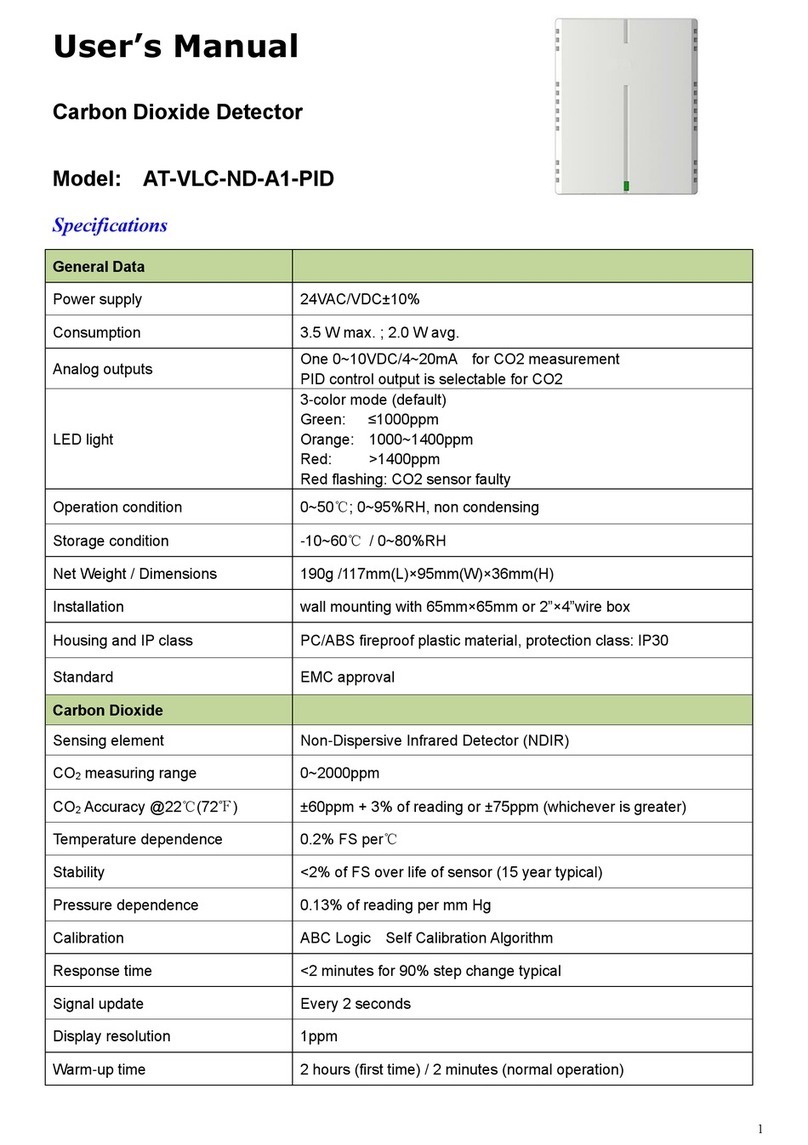
Ricoh R3111x Series User manual

R3111x SERIES
LOW VOLTAGE DETECTOR
NO.EA-056-110408
1
OUTLINE
The R3111x series are CMOS-based voltage detector ICs with high detector threshold accuracy and ultra-low
supply current, which can be operated at an extremely low voltage and is used for system reset as an example.
Each of these ICs consists of a voltage reference unit, a comparator, resistors for detector threshold setting,
an output driver and a hysteresis circuit. The detector threshold is fixed with high accuracy internally and does
not require any adjustment.
Three output types, Nch open drain “L” type, Nch open drain “H” type and CMOS type are available.
The R3111x Series are operable at a lower voltage than that for the Rx5VL series, and can be driven by a
single battery.
Seven types of packages, TO-92 (Limited), SOT-89, SOT-23-3, SOT-23-5, SC-82AB, SC-88A and
SON1612-6 are available.
FEATURES
•Supply Current......................................................................Typ. 0.8μA (-VDET=1.5V, VDD=-VDET−0.1V)
•Operating Voltage Range......................................................0.7V to 10.0V (Topt=25°C)
•Detector Threshold Range....................................................0.9V to 6.0V (0.1V steps)
(
For other voltages, please refer to MARK INFORMATIONS.)
•Detector Threshold Accuracy................................................±2.0%
•Temperature-Drift Coefficient of Detector Threshold ............Typ. ±100ppm/°C
•Output Types.........................................................................Nch Open Drain “L”, Nch Open Drain “H”, and
CMOS
•Packages ..............................................................................SON1612-6, SC-82AB, SC-88A, SOT-23-3,
SOT-23-5,SOT-89,TO-92(Limited)
APPLICATIONS
•CPU and Logic Circuit Reset
•Battery Checker
•Window Comparator
•Wave Shaping Circuit
•Battery Back-up Circuit
•Power Failure Detector

R3111x
2
BLOCK DIAGRAMS
R3111xxxxA R3111xxxxB
OUT
V
DD
Vref
GND
OUT
V
DD
Vref
GND
R3111xxxxC
OUT
V
DD
GND
Vref

R3111x
3
SELECTION GUIDE
The package type, the detector threshold, the output type and the taping type for the ICs can be selected at
the users’ request. The selection can be made with designating the part number as shown below;
Product Name Package Quantity per Reel Pb Free Halogen Free
R3111Dxx1∗-TR-FE SON1612-6 4,000 pcs Yes Yes
R3111Qxx1∗-TR-FE SC-82AB 3,000 pcs Yes Yes
R3111Qxx2∗-TR-FE SC-88A 3,000 pcs Yes Yes
R3111Nxx2$-TR-FE SOT-23-3 3,000 pcs Yes Yes
R3111Nxx1$-TR-FE SOT-23-5 3,000 pcs Yes Yes
R3111Hxx1$-T1-FE SOT-89 1,000 pcs Yes Yes
R3111Exx1$-TZ-F TO-92 (Limited) 2,500 pcs Yes No
xx: The detector threshold can be designated in the range from 0.9V(09) to 6.0V(60) in 0.1V steps.
(For other voltages, please refer to MARK INFORMATIONS.)
∗: Designation of Output Type
(A) Nch Open Drain (Output "L" at Detection)
(B) Nch Open Drain (Output "H" at Detection)
(C) CMOS (Output "L" at Detection)
$ : Designation of Output Type
(A) Nch Open Drain (Output "L" at Detection)
(C) CMOS (Output "L" at Detection)
The products scheduled to be discontinued (be sold to limited customer) : "Limited"
These products will be discontinued in the future. You can not select these products newly.
We will provide these products to the customer who has been using or has ordered them before.
But we recommend changing to other products as soon as possible.

R3111x
4
PIN CONFIGURATIONS
zTO-92 zSOT-89 zSOT-23-3 zSOT-23-5
3
12
(mark side)
3
12
(mark side)
12
3
(mark side)
123
4
5
(mark side)
zSC-82AB zSC-88A zSON1612-6
4 3
12
(mark side)
5 4
13
2
(mark side)
123
654
(mark side)
PIN DESCRIPTIONS
zTO-92 (Limited) zSOT-89 zSOT-23-3 zSOT-23-5
Pin No. Symbol Pin No. Symbol Pin No. Symbol Pin No. Symbol
1 VDD 1 OUT 1 OUT 1 OUT
2 GND
2 VDD 2 GND 2 VDD
3 OUT
3 GND 3 VDD 3 GND
4 NC
5 NC
zSC-82AB zSC-88A zSON1612-6
Pin No. Symbol Pin No. Symbol Pin No. Symbol
1 OUT 1 OUT 1 OUT
2 VDD 2 NC 2 VDD
3 NC 3 VDD 3 GND
4 GND 4 NC 4 NC
5 GND 5 VDD
6 NC

R3111x
5
ABSOLUTE MAXIMUM RATINGS
Symbol Item Rating Unit
VDD Supply Voltage 12 V
VOUT1 Output Voltage (CMOS) VSS−0.3 to VDD+0.3 V
VOUT2 Output Voltage (Nch) VSS−0.3 to 12 V
IOUT Output Current 70 mA
Power Dissipation (TO-92)* (Limited) 300
Power Dissipation (SOT-89)* 900
Power Dissipation (SOT-23-3)* 420
Power Dissipation (SOT-23-5)* 420
Power Dissipation (SC-82AB)* 380
Power Dissipation (SC-88A)* 380
PD
Power Dissipation (SON1612-6)* 500
mW
Topt Operating Temperature Range −40 to 85 °C
Tstg Storage Temperature Range −55 to 125 °C
Tsolder Lead temperature (Soldering) 260°C, 10s
* )For Power Dissipation, please refer to PACKAGE INFORMATION.
ABSOLUTE MAXIMUM RATINGS
Electronic and mechanical stress momentarily exceeded absolute maximum ratings may cause the
permanent damages and may degrade the life time and safety for both device and system using the device
in the field. The functional operation at or over these absolute maximum ratings is not assured.
RECOMMENDED OPERATING CONDITIONS (ELECTRICAL CHARACTERISTICS)
All of electronic equipment should be designed that the mounted semiconductor devices operate within the
recommended operating conditions. The semiconductor devices cannot operate normally over the
recommended operating conditions, even if when they are used over such conditions by momentary
electronic noise or surge. And the semiconductor devices may receive serious damage when they continue
to operate over the recommended operating conditions.

R3111x
6
ELECTRICAL CHARACTERISTICS
•R3111x09xA/C Topt=25°C
Symbol Item Conditions Min. Typ. Max. Unit
-VDET Detector Threshold 0.882 0.900 0.918 V
VHYS Detector Threshold Hysteresis 0.027 0.045 0.063 V
ISS Supply Current VDD=0.80V
VDD=2.90V 0.8
0.9 2.4
2.7 μA
VDDH Maximum Operating Voltage 10 V
Topt=25°C 0.55 0.70
VDDL Minimum Operating Voltage∗Note1 −40°C
<
=
Topt
<
=
85°C 0.65 0.80 V
Nch
VDS=0.05V,VDD=0.70V
VDS=0.50V,VDD=0.85V
0.01
0.05
0.05
0.50
mA
IOUT Output Current (Driver Output Pin) Pch
VDS=−2.1V,VDD=4.5V
1.0
2.0 mA
tPLH Output Delay Time∗Note2 100
μs
Δ-VDET/
ΔTopt Detector Threshold Temperature
Coefficient −40°C
<
=
Topt
<
=
85°C ±100 ppm/°C
•R3111x18xA/C Topt=25°C
Symbol Item Conditions Min. Typ. Max. Unit
-VDET Detector Threshold 1.764 1.800 1.836 V
VHYS Detector Threshold Hysteresis 0.054 0.090 0.126 V
ISS Supply Current VDD=1.70V
VDD=3.80V 0.8
1.0 2.4
3.0 μA
VDDH Maximum Operating Voltage 10 V
Topt=25°C 0.55 0.70
VDDL Minimum Operating Voltage∗Note1 −40°C
<
=
Topt
<
=
85°C 0.65 0.80 V
Nch
VDS=0.05V, VDD=0.70V
VDS=0.50V, VDD=1.50V
0.01
1.00
0.05
2.00
mA
IOUT Output Current (Driver Output Pin) Pch
VDS=−2.1V,VDD=4.5V
1.0
2.0 mA
tPLH Output Delay Time∗Note2 100
μs
Δ-VDET/
ΔTopt Detector Threshold Temperature
Coefficient −40°C
<
=
Topt
<
=
85°C ±100 ppm/°C
∗Note1:
Minimum operating voltage means the value of input voltage when output voltage maintains 0.1V or less. (In
the case of Nch Open Drain Output type, the output pin is pulled up with a resistance of 470k
Ω
to 5.0V.)
∗Note2:In the case of CMOS Output type: The time interval between the rising edge of VDD input pulse from 0.7V
to (+VDET)+2.0V and output voltage level becoming to ((+VDET)+2.0V)/2.
In the case of Nch Open Drain Output type: The output pin is pulled up with a resistance of 470kΩto
5.0V, the time interval between the rising edge of VDD input pulse from 0.7V to (+VDET)+2.0V and output
voltage level becoming to 2.5V.

R3111x
7
•R3111x27xA/C Topt=25°C
Symbol Item Conditions Min. Typ. Max. Unit
-VDET Detector Threshold 2.646 2.700 2.754 V
VHYS Detector Threshold Hysteresis 0.081 0.135 0.189 V
ISS Supply Current VDD=2.60V
VDD=4.70V 0.9
1.1 2.7
3.3 μA
VDDH Maximum Operating Voltage 10 V
Topt=25°C 0.55 0.70
VDDL Minimum Operating Voltage∗Note1 −40°C
<
=
Topt
<
=
85°C 0.65 0.80 V
Nch
VDS=0.05V,VDD=0.70V
VDS=0.50V,VDD=1.50V
0.01
1.00
0.05
2.00 mA
IOUT Output Current (Driver Output Pin) Pch
VDS=−2.1V,VDD=4.5V
1.0
2.0 mA
tPLH Output Delay Time∗Note2 100
μs
Δ-VDET/
ΔTopt Detector Threshold Temperature
Coefficient −40°C
<
=
Topt
<
=
85°C ±100 ppm/°C
•R3111x36xA/C Topt=25°C
Symbol Item Conditions Min. Typ. Max. Unit
-VDET Detector Threshold 3.528 3.600 3.672 V
VHYS Detector Threshold Hysteresis 0.108 0.180 0.252 V
ISS Supply Current VDD= 3.47V
VDD= 5.60V 1.0
1.2 3.0
3.6 μA
VDDH Maximum Operating Voltage 10 V
Topt=25°C 0.55 0.70
VDDL Minimum Operating Voltage∗Note1 −40°C
<
=
Topt
<
=
85°C 0.65 0.80 V
Nch
VDS=0.05V,VDD=0.70V
VDS=0.50V,VDD=1.50V
0.01
1.00
0.05
2.00
mA
IOUT Output Current (Driver Output Pin) Pch
VDS=−2.1V,VDD=4.5V
1.0
2.0 mA
tPLH Output Delay Time∗Note2 100
μs
Δ-VDET/
ΔTopt Detector Threshold Temperature
Coefficient −40°C
<
=
Topt
<
=
85°C ±100 ppm/°C
∗Note1:
Minimum operating voltage means the value of input voltage when output voltage maintains 0.1V or less. (In
the case of Nch Open Drain Output type, the output pin is pulled up with a resistance of 470k
Ω
to 5.0V.)
∗Note2:In the case of CMOS Output type: The time interval between the rising edge of VDD input pulse from 0.7V
to (+VDET)+2.0V and output voltage level becoming to ((+VDET)+2.0V)/2.
In the case of Nch Open Drain Output type: The output pin is pulled up with a resistance of 470kΩto
5.0V, the time interval between the rising edge of VDD input pulse from 0.7V to (+VDET)+2.0V and output
voltage level becoming to 2.5V.

R3111x
8
•R3111x45xA/C Topt=25°C
Symbol Item Conditions Min. Typ. Max. Unit
-VDET Detector Threshold 4.410 4.500 4.590 V
VHYS Detector Threshold Hysteresis 0.135 0.225 0.315 V
ISS Supply Current VDD=4.34V
VDD=6.50V 1.1
1.3 3.3
3.9 μA
VDDH Maximum Operating Voltage 10 V
Topt=25°C 0.55 0.70
VDDL Minimum Operating Voltage∗Note1 −40°C
<
=
Topt
<
=
85°C 0.65 0.80 V
Nch
VDS=0.05V, VDD=0.70V
VDS=0.50V, VDD=1.50V
0.01
1.00
0.05
2.00 mA
IOUT Output Current (Driver Output Pin) Pch
VDS=−2.1V,VDD=8.0V
1.5
3.0 mA
tPLH Output Delay Time∗Note2 100
μs
Δ-VDET/
ΔTopt Detector Threshold Temperature
Coefficient −40°C
<
=
Topt
<
=
85°C ±100 ppm/°C
•R3111x54xA/C Topt=25°C
Symbol Item Conditions Min. Typ. Max. Unit
-VDET Detector Threshold 5.292 5.400 5.508 V
VHYS Detector Threshold Hysteresis 0.162 0.270 0.378 V
ISS Supply Current VDD=5.20V
VDD=7.40V
1.2
1.4 3.6
4.2 μA
VDDH Maximum Operating Voltage 10 V
Topt=25°C 0.55 0.70
VDDL Minimum Operating Voltage∗Note1 −40°C
<
=
Topt
<
=
85°C 0.65 0.80 V
Nch
VDS=0.05V, VDD=0.70V
VDS=0.50V, VDD=1.50V
0.01
1.00
0.05
2.00 mA
IOUT Output Current
(Driver Output Pin) Pch
VDS=−2.1V, VDD=8.0V
1.5
3.0 mA
tPLH Output Delay Time∗Note2 100
μs
Δ-VDET/
ΔTopt Detector Threshold Temperature
Coefficient −40°C
<
=
Topt
<
=
85°C ±100 ppm/°C
∗Note1:
Minimum operating voltage means the value of input voltage when output voltage maintains 0.1V or less. (In
the case of Nch Open Drain Output type, the output pin is pulled up with a resistance of 470k
Ω
to 5.0V.)
∗Note2:In the case of CMOS Output type: The time interval between the rising edge of VDD input pulse from 0.7V
to (+VDET)+2.0V and output voltage level becoming to ((+VDET)+2.0V)/2.
In the case of Nch Open Drain Output type: The output pin is pulled up with a resistance of 470kΩto
5.0V, the time interval between the rising edge of VDD input pulse from 0.7V to (+VDET)+2.0V and output
voltage level becoming to 2.5V.

R3111x
9
•R3111Q231B Topt=25°C
Symbol Item Conditions Min. Typ. Max. Unit
-VDET Detector Threshold 2.254 2.300 2.346 V
VHYS Detector Threshold Hysteresis 0.069 0.115 0.161 V
ISS Supply Current VDD=2.2V
VDD=4.3V 0.9
1.1 2.7
3.3 μA
VDDH Maximum Operating Voltage 10 V
Topt=25°C 0.55 0.70
VDDL Minimum Operating Voltage∗Note1 −40°C
<
=
Topt
<
=
85°C 0.65 0.80 V
IOUT Output Current (Driver Output Pin) Nch
VDS=0.10V,VDD=6.5V 2.5 mA
tPLH Output Delay Time∗Note2 100
μs
Δ-VDET/
ΔTopt Detector Threshold Temperature
Coefficient −40°C
<
=
Topt
<
=
85°C ±100 ppm/°C
•R3111Q441B Topt=25°C
Symbol Item Conditions Min. Typ. Max. Unit
-VDET Detector Threshold 4.312 4.400 4.488 V
VHYS Detector Threshold Hysteresis 0.132 0.220 0.308 V
ISS Supply Current VDD=4.24V
VDD=6.4V
1.1
1.3 3.3
3.9 μA
VDDH Maximum Operating Voltage 10 V
Topt=25°C 0.55 0.70
VDDL Minimum Operating Voltage∗Note1 −40°C
<
=
Topt
<
=
85°C 0.65 0.80 V
IOUT Output Current
(Driver Output Pin) Nch
VDS=0.10V, VDD=6.5V 2.5 mA
tPLH Output Delay Time∗Note2 100
μs
Δ-VDET/
ΔTopt Detector Threshold Temperature
Coefficient −40°C
<
=
Topt
<
=
85°C ±100 ppm/°C
∗Note1:
Minimum operating voltage means the value of input voltage when output voltage maintains 0.1V or less. (In
the case of Nch Open Drain Output type, the output pin is pulled up with a resistance of 470k
Ω
to 5.0V.)
∗Note2:In the case of CMOS Output type: The time interval between the rising edge of VDD input pulse from 0.7V
to (+VDET)+2.0V and output voltage level becoming to ((+VDET)+2.0V)/2.
In the case of Nch Open Drain Output type: The output pin is pulled up with a resistance of 470kΩto
5.0V, the time interval between the rising edge of VDD input pulse from 0.7V to (+VDET)+2.0V and output
voltage level becoming to 2.5V.

R3111x
10
TIMING CHART
Detector Threshold
t
PLH
t
PLH
t
PLH
GND
GND
V
DDL
-V
DET
+V
DET
Detector Threshold
Released Voltage
Minimum Operating Voltage
Pull-up Voltage
Supply
Voltage
(V
DD
)
Output
Voltage
(V
OUT
)
R3111xxxxA R3111xxxxB R3111xxxxC
Detector Threshold Detector Threshold
Hysteresis HysteresisHysteresis
DEFINITION OF OUTPUT DELAY TIME
Output Delay Time (tPLH) is defined as follows:
1. In the case of Nch Open Drain Output:(R3111xxxxA/B)
Under the condition of the output pin (OUT) is pulled up through a resistor of 470kΩto 5V, the time interval
between the rising edge of VDD pulse from 0.7V to (+VDET)+2.0V and becoming of the output voltage to 2.5V.
2. In the case of CMOS Output:(R3111xxxxC)
The time interval between the rising edge of VDD pulse from 0.7V to (+VDET)+2.0V and becoming of the output
voltage to ((+VDET)+2.0V)/2.
+V
DET
+2.0V
0.7V
Supply
Voltage
(V
DD
) GND
5.0V
2.5V
GND
Output
Voltage
(V
OUT
)
t
PLH
t
PHL
+V
DET
+
2.0V
0.7V
GND
5.0V
2.5V
GND
t
PLH
t
PHL
Supply
Voltage
(V
DD
)
Output
Voltage
(V
OUT
)
+
V
DET
+2.0V
0.7V
GND
GND
t
PLH
t
PHL
+
V
DET
+2.0V
+
V
DET
+2.0V
2
Supply
Voltage
(V
DD
)
Output
Voltage
(V
OUT
)
Nch Open Drain Output Nch Open Drain Output CMOS Output
(R3111xxxxA) (R3111xxxxB) (R3111xxxxC)

R3111x
11

R3111x
12
ELECTRICAL CHARACTERISTICS BY DETECTOR THRESHOLD
•R3111x09x to R3111x60x
Detector Threshold Detector Threshold
Hysteresis Supply Current 1 Supply Current 2
-VDET[V]V
HYS[V]ISS1[μA]I
SS2[μA]
Part
Number Min. Typ. Max. Min. Typ. Max. Condition Typ. Max. Condition Typ. Max.
R3111x09xx 0.882 0.900 0.918 0.027 0.045 0.063 0.9 2.7
R3111x10xx 0.980 1.000 1.020 0.030 0.050 0.070
R3111x11xx 1.078 1.100 1.122 0.033 0.055 0.077
R3111x12xx 1.176 1.200 1.224 0.036 0.060 0.084
R3111x13xx 1.274 1.300 1.326 0.039 0.065 0.091
R3111x14xx 1.372 1.400 1.428 0.042 0.070 0.098
R3111x15xx 1.470 1.500 1.530 0.045 0.075 0.105
R3111x16xx 1.568 1.600 1.632 0.048 0.080 0.112
R3111x17xx 1.666 1.700 1.734 0.051 0.085 0.119
R3111x18xx 1.764 1.800 1.836 0.054 0.090 0.126
R3111x19xx 1.862 1.900 1.938 0.057 0.095 0.133
0.8 2.4 1.0 3.0
R3111x20xx 1.960 2.000 2.040 0.060 0.100 0.140
R3111x21xx 2.058 2.100 2.142 0.063 0.105 0.147
R3111x22xx 2.156 2.200 2.244 0.066 0.110 0.154
R3111x23xx 2.254 2.300 2.346 0.069 0.115 0.161
R3111x24xx 2.352 2.400 2.448 0.072 0.120 0.168
R3111x25xx 2.450 2.500 2.550 0.075 0.125 0.175
R3111x26xx 2.548 2.600 2.652 0.078 0.130 0.182
R3111x27xx 2.646 2.700 2.754 0.081 0.135 0.189
R3111x28xx 2.744 2.800 2.856 0.084 0.140 0.196
R3111x29xx 2.842 2.900 2.958 0.087 0.145 0.203
VDD=
(-VDET)
−0.10V
0.9 2.7 1.1 3.3
R3111x30xx 2.940 3.000 3.060 0.090 0.150 0.210
R3111x31xx 3.038 3.100 3.162 0.093 0.155 0.217
R3111x32xx 3.136 3.200 3.264 0.096 0.160 0.224
R3111x33xx 3.234 3.300 3.366 0.099 0.165 0.231
R3111x34xx 3.332 3.400 3.468 0.102 0.170 0.238
R3111x35xx 3.430 3.500 3.570 0.105 0.175 0.245
R3111x36xx 3.528 3.600 3.672 0.108 0.180 0.252
R3111x37xx 3.626 3.700 3.774 0.111 0.185 0.259
R3111x38xx 3.724 3.800 3.876 0.114 0.190 0.266
R3111x39xx 3.822 3.900 3.978 0.117 0.195 0.273
VDD=
(-VDET)
−0.13V 1.0 3.0 1.2 3.6
R3111x40xx 3.920 4.000 4.080 0.120 0.200 0.280
R3111x41xx 4.018 4.100 4.182 0.123 0.205 0.287
R3111x42xx 4.116 4.200 4.284 0.126 0.210 0.294
R3111x43xx 4.214 4.300 4.386 0.129 0.215 0.301
R3111x44xx 4.312 4.400 4.488 0.132 0.220 0.308
R3111x45xx 4.410 4.500 4.590 0.135 0.225 0.315
R3111x46xx 4.508 4.600 4.692 0.138 0.230 0.322
R3111x47xx 4.606 4.700 4.794 0.141 0.235 0.329
R3111x48xx 4.704 4.800 4.896 0.144 0.240 0.336
R3111x49xx 4.802 4.900 4.998 0.147 0.245 0.343
VDD=
(-VDET)
−0.16V 1.1 3.3 1.3 3.9
R3111x50xx 4.900 5.000 5.100 0.150 0.250 0.350
R3111x51xx 4.998 5.100 5.202 0.153 0.255 0.357
R3111x52xx 5.096 5.200 5.304 0.156 0.260 0.364
R3111x53xx 5.194 5.300 5.406 0.159 0.265 0.371
R3111x54xx 5.292 5.400 5.508 0.162 0.270 0.378
R3111x55xx 5.390 5.500 5.610 0.165 0.275 0.385
R3111x56xx 5.488 5.600 5.712 0.168 0.280 0.392
R3111x57xx 5.586 5.700 5.814 0.171 0.285 0.399
R3111x58xx 5.684 5.800 5.916 0.174 0.290 0.406
R3111x59xx 5.782 5.900 6.018 0.177 0.295 0.413
R3111x60xx 5.880 6.000 6.120 0.180 0.300 0.420
VDD=
(-VDET)
−0.20V 1.2 3.6
VDD=
(-VDET)
+2.0V
1.4 4.2
*1)
In the case of CMOS output type; when the voltage is forced to V
DD
from 0.7V to (
+
V
DET
)
+
2.0V, time interval between the rising edge of V
DD
and the reaching point at
((
+
V
DET
)
+
2.0V)/2. In the case of Nch open drain output type : The output pin is pulled up to 5V through 470k
Ω
, and when the voltage is forced to V
DD
from 0.7V to
(
+
V
DET
)
+
2.0V, time interval between the rising edge of VDD and the reaching point at ((
+
V
DET
)
+
2.0V)/2.
*2) VDD value when Output Voltage is equal or less than 0.1V. In the case of Nch open drain output type, the output pin is pulled up to 5V through 470kΩ
resistor.
Condition 1: Topt=25°C
Condition 2: −40°C
<
=
Topt
<
=
85°C

R3111x
13
Output Current 1 Output Current 2 *3Output Delay
Time
Minimum
Operating Voltage Detector Threshold
Temperature Coefficient
IOUT1[mA]I
OUT2[mA]tPLH[μs]VDDL[V]Δ-VDET/ΔTopt[ppm/°C]
Condition Min. Typ. Condition Min. Typ. Max. Typ. Max. Condition Typ.
VDD=
0.85V 0.05 0.5
VDD=
1.0V 0.2 1.0
<A/C version>
Nch
VDS=0.05V
VDD=0.7V
<B version>
Nch
VDS=0.10V
VDD=6.5V
0.01
2.5
0.05
-
Nch
VDS=
0.5V
VDD=
1.5V
1.0
2.0 100 *1
*2
Condition 1
0.55
Condition 2
0.65
*2
Condition 1
0.70
Condition 2
0.80
−40°C
<
=
Topt
<
=
85°C ±100
*3) Only A/C versions.

R3111x
14
OPERATION
•Operation of R3111xxxxA
Vref
Ra
Rb
Rc
V
DD
OUT
GND
Tr.1 Nch
Com
p
arato
r
OUT pin should be pulled-up to
V
DD
or an external voltage level.
Block Diagram (R3111xxxxA)
13 5
A B
t
PLH
2 4
GND
GND
VDDL
-
VDET
+VDET
Detector Threshold
Released Voltage
Minimum Operating Voltage
Pull-up Voltage
Detector Threshold
Hysteresis
Supply Voltage
(V
DD
)
Output Voltage
(V
OUT
)
Step 1 2 3 4 5
Comparator (
+
)
Pin Input Voltage I II II II I
Comparator Output H L Indefinite L H
Tr.1 OFF ON Indefinite ON OFF
Output Tr. Nch OFF ON Indefinite ON OFF
I×V
DD
Rb+Rc
Ra+Rb+Rc
II ×V
DD
Rb
Ra+Rb
Operation Diagram
•Explanation of operation
Step 1. The output voltage is equal to the pull-up voltage.
Step 2. At Point “A”, Vref
>
=
VDD×(Rb+Rc)/(Ra+Rb+Rc) is true, as a result, the output of comparator is reversed
from "H" to "L", therefore the output voltage becomes the GND level. The voltage level of Point Ameans
a detector threshold voltage (−VDET).
Step 3. When the supply voltage is lower than the minimum operating voltage, the operation of the output
transistor becomes indefinite. The output voltage is equal to the pull-up voltage.
Step 4. The output Voltage is equal to the GND level.
Step 5. At Point “B”, Vref
<
=
VDD×Rb/(Ra+Rb) is true, as a result, the output of comparator is reversed from "L" to
"H", then the output voltage is equal to the pull-up voltage. The voltage level of Point B means a released
voltage (+VDET).
∗) The difference between a released voltage and a detector threshold voltage is a detector threshold hysteresis.
Output
Delay Time

R3111x
15
•Operation of R3111xxxxB
Vref
Ra
Rb
Rc
V
DD
OUT
GND
Tr.1 Nch
Com
p
arator
OUT pin should be pulled-up to
V
DD
or an external voltage level.
Block Diagram (R3111xxxxB)
t
PLH
GND
GND
VDDL
-
VDET
+VDET
Detector Threshold
Released Voltage
Minimum Operating Voltage
Pull-up Voltage
1 2 3
A B
Detector Threshold
Hysteresis
Supply Voltage
(VDD)
Output Voltage
(VOUT)
Step 1 2 3
Comparator (−)
Pin Input Voltage I II I
Comparator Output L H L
Tr.1 OFF ON OFF
Output Tr. Nch ON OFF ON
I×V
DD
Rb+Rc
Ra+Rb+Rc
II ×V
DD
Rb
Ra+Rb
Operation Diagram
•Explanation of operation
Step 1. The output voltage is equal to the GND level.
Step 2. At Point “A”, Vref
>
=
VDD×(Rb+Rc)/(Ra+Rb+Rc) is true, as a result, the output of comparator is reversed
from "L" to "H", therefore the output voltage becomes the pull-up voltage. The voltage level of Point A
means a detector threshold voltage (−VDET).
Step 3. At Point “B”, Vref
<
=
VDD×Rb/(Ra+Rb) is true, as a result, the output of comparator is reversed from "H" to
"L", then the output voltage is equal to the GND level. The voltage level of Point B means a released
voltage (+VDET).
∗) The difference between a released voltage and a detector threshold voltage is a detector threshold hysteresis.
Output
Delay Time

R3111x
16
•Operation of R3111xxxxC
Vref
Ra
Rb
Rc
VDD
OUT
GND
Tr.1 Nch
Pch
Com
p
arato
r
Block Diagram (R3111xxxxC)
t
PLH
GND
GND
V
DDL
-
V
DET
+V
DET
Detector Threshold
Released Voltage
Minimum Operating Voltage
123 45
A B
Detector Threshold
Hysteresis
Supply Voltage
(V
DD
)
Output Voltage
(V
OUT
)
Step 1 2 3 4 5
Comparator (+)
Pin Input Voltage I II II II I
Comparator Output H L Indefinite L H
Tr.1 OFF ON Indefinite ON OFF
Pch ON OFF Indefinite OFF ON
Output Tr. Nch OFF ON Indefinite ON OFF
I×V
DD
Rb+Rc
Ra+Rb+Rc
II ×V
DD
Rb
Ra+Rb
Operation Diagram
•Explanation of operation
Step 1. The output voltage is equal to the supply voltage (VDD).
Step 2. At Point “A”, Vref
>
=
VDD×(Rb+Rc)/(Ra+Rb+Rc) is true, as a result, the output of comparator is reversed
from "H" to "L", therefore the output voltage becomes the GND level. The voltage level of Point A
means a detector threshold voltage (−VDET).
Step 3. When the supply voltage is lower than the minimum operating voltage, the operation of the output
transistor becomes indefinite.
Step 4. The output Voltage is equal to the GND level.
Step 5. At Point “B”, Vref
<
=
VDD×Rb/(Ra+Rb) is true, as a result, the output of comparator is reversed from "L" to
"H", then the output voltage is equal to the supply voltage (VDD). The voltage level of Point B means a
released voltage (+VDET).
∗) The difference between a released voltage and a detector threshold voltage is a detector threshold hysteresis.
Output
Delay Time

R3111x
17
TEST CIRCUITS
GND
V
DD
V
IN
I
SS
R3111x
Series OUT
GND
V
DD
V
IN
R3111x
Series OUT
470kΩ
5V
V
OUT
Supply Current Test Circuit Detector Threshold Test Circuit
(Pull-up circuit is not necessary for
CMOS Output type.)
GND
V
DD
V
IN
R3111x
Series OUT V
DS
I
OUT
GND
V
DD
V
IN
R3111x
Series OUT V
DD
−
V
DS
I
OUT
V
DS
Nch Driver Output Current Test Circuit Pch Driver Output Current Test Circuit
∗Apply to CMOS Output type only
GND
V
DD
R3111x
Series OUT
V
DS
V
OUT
5V
R
OUT
470kΩ
P.G.
+V
DET
+2.0V
0.7V
GND
C
OUT
GND
V
DD
R3111x
Series OUT
V
DS
V
OUT
5V
R
OUT
470kΩ
P.G.
+V
DET
+2.0V
0.7V
GND
R
IN
470kΩ
C
IN
Output Delay Time Test Circuit (1) Output Delay Time Test Circuit (2)
(Pull-up circuit is not necessary for
CMOS Output type.)

R3111x
18
TYPICAL CHARACTERISTICS
1) Supply Current vs. Input Voltage
R3111x09xx R3111x27xx
Topt=85°C
25°C
-40°C
2.5
2.0
1.5
1.0
0.5
0.0
Input Voltage V
IN
(V)
0246810
Supply Current I
SS
(μA)
Topt=85°C
25°C
-40°C
2.0
1.5
1.0
0.5
0.0
Input Voltage V
IN
(V)
0246810
Supply Current I
SS
(μA)
R3111x45xx
Topt=85°C
25°C
-40°C
2.0
1.5
1.0
0.5
0.0
Input Voltage V
IN
(V)
0246810
Supply Current I
SS
(μA)
2) Detector Threshold Hysteresis vs. Temperature
R3111x09xx R3111x27xx
+VDET
-VDET
1.00
0.98
0.96
0.94
0.92
0.90
0.88
0.84
0.86
Temperature Topt(°C)
-60 0 20406080-40 -20 100
Detector Threshold -VDET(V)
2.9
2.8
2.7
2.6
2.5
+VDET
-VDET
Temperature Topt(°C)
-60 0 20406080-40 -20 100
Detector Threshold -VDET(V)

R3111x
19
R3111x45xx
4.8
4.7
4.6
4.5
4.4
+VDET
-VDET
Temperature Topt(°C)
-60 0 20406080-40 -20 100
Detector Threshold -VDET(V)
3) Output Voltage vs. Input Voltage
R3111x09xC R3111x09xA
Topt=-40°C
25°C
85°C
1.6
1.4
1.2
1.0
0.8
0.6
0.4
0.0
0.2
Input Voltage V
IN
(V)
0 0.6 0.8 1 1.2 1.40.2 0.4 1.6
Output Voltage V
OUT
(V)
5V Pull-up 470kΩ
6
5
4
3
2
0
1
Input Voltage VIN(V)
0 0.6 0.8 1 1.2 1.40.2 0.4 1.6
Output Voltage VOUT(V)
Topt=-40°C
25°C
85°C
R3111x27xC R3111x27xA
Topt=-40°C
25°C
85°C
4.0
3.5
3.0
2.5
2.0
1.5
1.0
0.0
0.5
Input Voltage VIN(V)
0 1.5 2 2.5 3 3.50.5 1 4
Output Voltage VOUT(V)
5V Pull-up 470kΩ
6
5
4
3
2
0
1
Input Voltage V
IN
(V)
0 1.5 2 2.5 3 3.50.5 1 4
Output Voltage V
OUT
(V)
Topt=-40°C
25°C
85°C

R3111x
20
R3111x45xC R3111x45xA
Topt=-40°C
25°C
85°C
6
5
4
3
2
0
1
Input Voltage V
IN
(V)
0231654
Output Voltage V
OUT
(V)
5V Pull-up 470kΩ
6
5
4
3
2
0
1
Input Voltage VIN(V)
0231654
Output Voltage VOUT(V)
Topt=-40°C
25°C
85°C
4) Nch Driver Output Current vs. VDS
R3111x09xx R3111x09xx
Topt=25°C
VDD=0.85V
0.7V
700
600
500
400
300
200
0
100
VDS(V)
0 0.2 0.4 0.6 0.8
Output Current IOUT(μA)
VDD=0.8V
0.7V
Topt=25°C
300
250
200
150
100
0
50
VDS(V)
0 0.02 0.04 0.06 0.08 0.1
Output Current IOUT(μA)
R3111x27xx R3111x27xx
Topt=25°C
VDD=2.5V
2.0V
1.5V
20
18
14
16
12
10
8
6
4
0
2
VDS(V)
0 0.5 1 1.5 2 2.5
Output Current IOUT(mA)
VDD=0.8V
0.7V
Topt=25°C
300
250
200
150
100
0
50
VDS(V)
0 0.02 0.04 0.06 0.08 0.1
Output Current IOUT(μA)
This manual suits for next models
1
Table of contents
Popular Security Sensor manuals by other brands

Protekt
Protekt LB100 instruction manual
Tatsuta Electric Wire & Cable
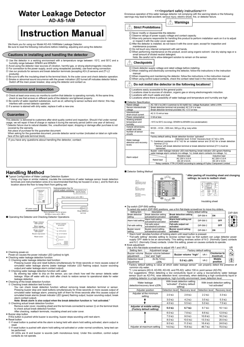
Tatsuta Electric Wire & Cable AD-AS-1AM instruction manual

Sensor Electronics
Sensor Electronics SEC 3000 Instruction and operation manual

hyfire
hyfire TAURUS TAU-OP-01-BL manual

WAVECONTROL
WAVECONTROL WaveMon user manual

Lince
Lince GR868 Bobby Installation, operation and maintenance manual
