Rise R653 User manual

PENTIUM II
ATX Form PCI & ISA Bus Pentium Mainboard
On Board PCI Master IDE, Multi-I/O.
_________________________________________________________________
Users Manual
※※※※※※※※※※※※※※※※※※※※※※※※※※※※※※※※※※※※

Table of Contents
Chapter 1 INTRODUCTION
1.1 Preface ................................................................................. 1-1
1.2 Key Features ........................................................................ 1-1
1.3 Static Electricity Precautions ............................................... 1-2
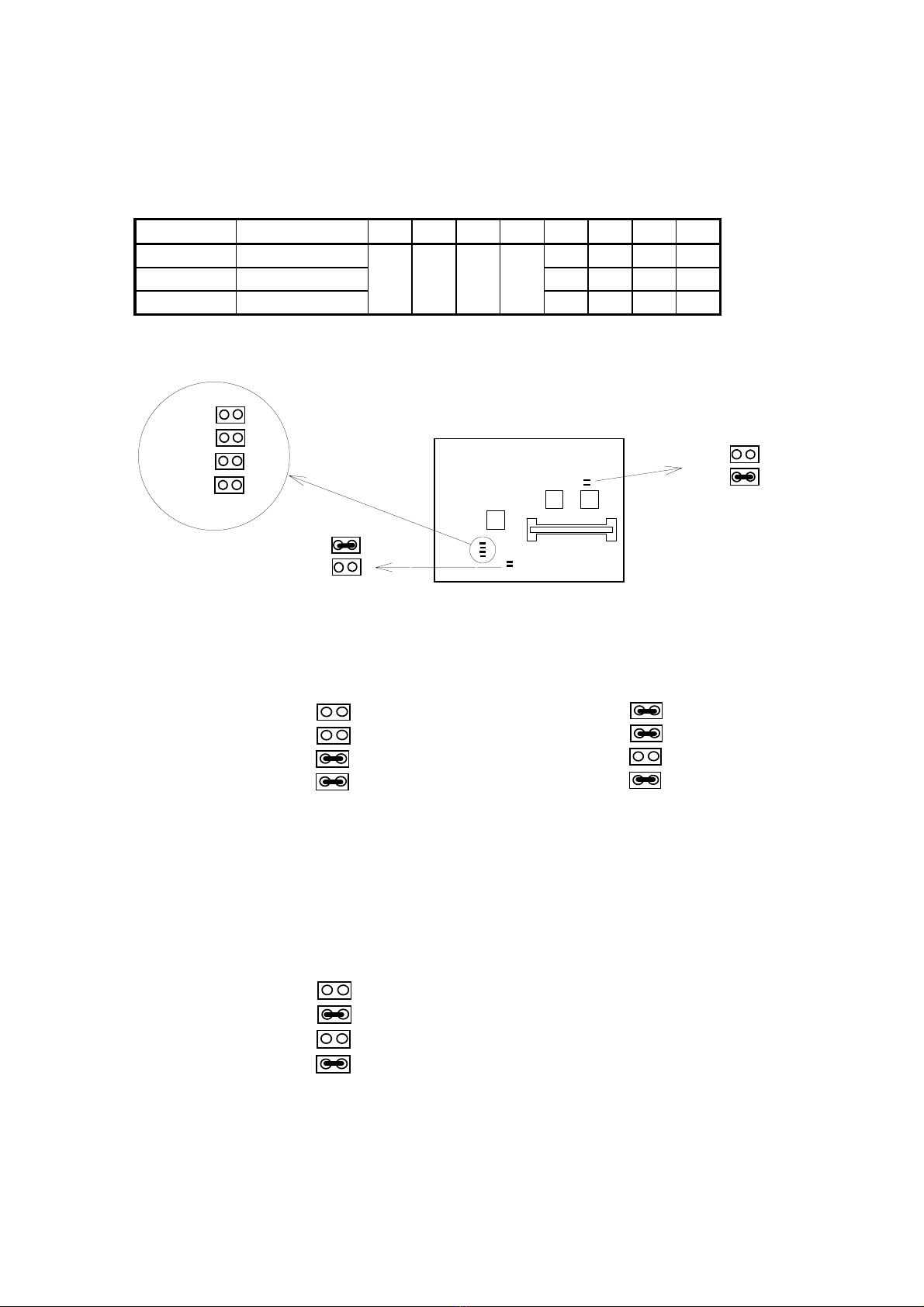
1.4 Mainboard Layout ................................................................ 1-3
Chapter 2 HARDWARE INSTALLATION
2.1 Jumper Setting Summary ................................................... 2-1
2.1.1 CPU Type Selector ................................................... 2-3
2.1.2 ATX Power ON/OFF Switch ...................................... 2-5
2.1.3 CMOS Clear Jumper ................................................. 2-5
2.1.4 Flash EPROM Voltage Selector ................................. 2-6
2.1.5 Upgrading System Memory ....................................... 2-7
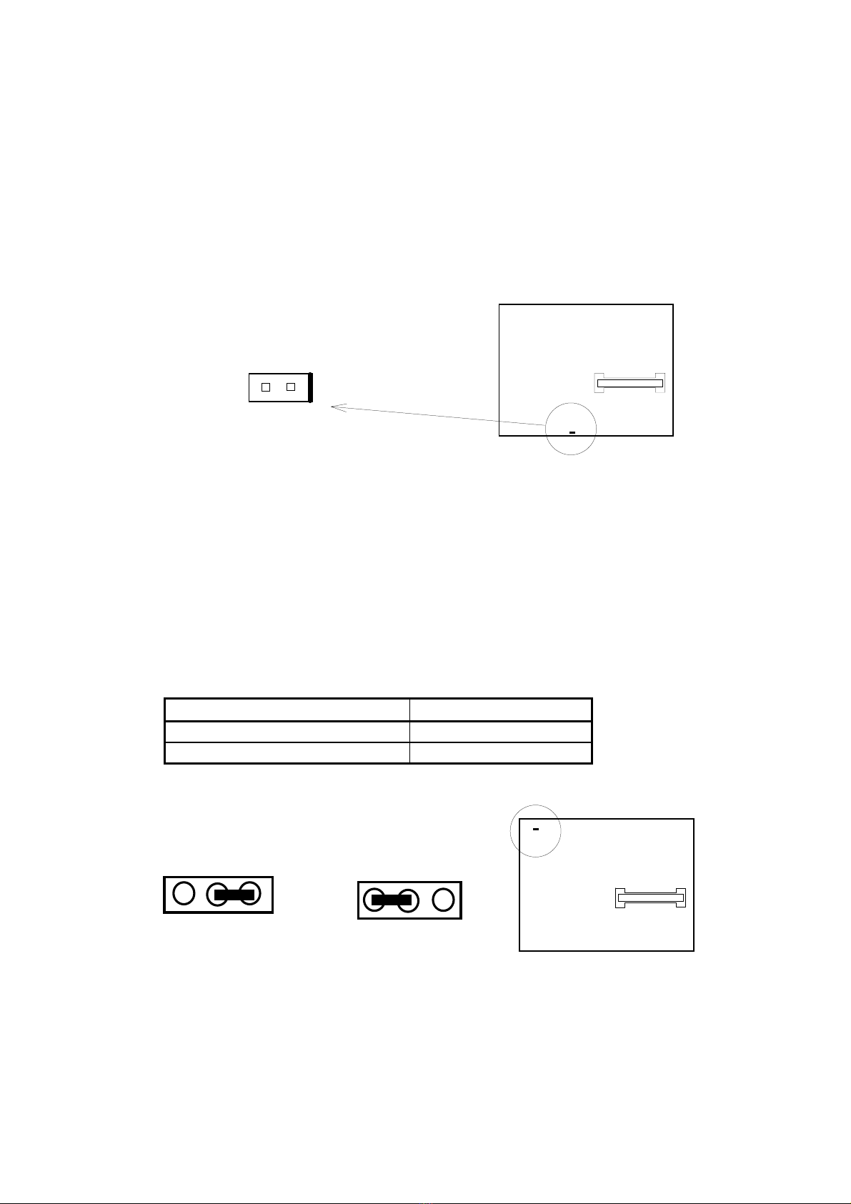
2.2 Connectors .......................................................................... 2-9
2.2.1 I/O Ports ................................................................... 2-10
2.2.2 External Connections ............................................... 2-11
Chapter 3 BIOS SETUP
3.1 Standard CMOS Setup ....................................................... 3-2
3.2 BIOS Feature Setup ........................................................... 3-3
3.3 Chipset Features Setup ..................................................... 3-6
3.4 Power Management Setup ................................................. 3-8
3.5 PNP/PCI Configuration Setup ............................................. 3-10
3.6 Load Setup Default ............................................................ 3-11
3.7 Integrated Peripherals ........................................................ 3-12
3.8 Supervisor Password ........................................................ 3-14
3.9 User Password ................................................................... 3-15
3.10 IDE HDD Auto Detection .................................................... 3-16

__________________________________【
【【
【1】
】】
】
1. INTRODUCTION
1.1. Preface
Welcom to use the R653 Pentium II system mainboard. This manual
explains how to use this mainboard and install upgrades. It has
overview of the design and features of the board and provides useful
information if you want to change the configuration of the board, or a
system it is installed in.
1.2. Key Features
The R653 Pentium II system mainboard is a high-performance system
board that support Intel Pentium II family CPUs.
There has many performance and system features integrated onto the
mainboard, including the following :
Supports Slot 1 for Intel Pentium II CPU 233MHz / 266MHz.
Chipset : Intel 82441FX, 82442FX, 82371SB.
Pentium II CPU Built-in 256K or 512KB L2 Cache.
Supports 3 Banks of SIMMs (Six -72PIN SIMM Sockets).
- Supports Memory Size from 8MB to 384MB.
- Supports Fast Page (FP) and Extended Data Out (EDO) Mode DRAM.
Four 16-bit ISA Slots and
Four 32-bit PCI Bus Master Mode Slots.
Fast PCI IDE Interface:
- Supports 2 PCI Bus Master IDE Ports. (up to Four IDE drivers)
- Supports PIO Mode 4 Transfers.
Universal Serial Bus Controller.
- Host / HUB Controller.
- Two USB Ports.
______________________________________________________________
1-1

【
【【
【1】
】】
】________________________________
On-board I / O support :
- 2 Serial Ports (6550 Fast UART compatible)
- 1 Parallel Port (with EPP and ECP capabilites)
- 1 Floppy Disk connector (support 2 FD drives).
- 1 PS/2 Mouse Connector.
- 1 PS/2 Keyboard Connector.
- 1 IrDA Connector.
BIOS support :
- Plug and Play (PnP), DMI, Green Function.
- 1M-bit Flash EPROM.
ATX Form Factor : 30.4cm x 24.4cm or 12" x 9.6" (4 Layers)
1.3. Static Electricity Precautions
Make sure you ground yourself before handling the mainboard or other
system components. Electrostatic discharge can easily damage the
components. Note that you must take special precaution when handling
the mainboard in dry or air-conditioned environments.
Take these precautions to protect you equipment from electrostatic
discharge :
zDo not remove the anti-static pachaging until you are ready to install
the system board and other system components.
zGround yourself before removing any system component from its
protective anti-static packaging. To ground yourself grasp the
expansion slot covers or other unpainted portions of the computer
chassis.
zFrequently ground yourself while working, or use a grounding strap.
zHandle the system board by the edges and avoid touching its
components.
______________________________________________________________
1-2

_________________________________【
【【
【1】
】】
】
1.4 R653 Mainboard Layout
KEYLOCK
SPEAK
RESET
HD LED
JP3
COM 1
Mouse
Keyboard
Printer
COM 2
JP4
JP5
JP6
TB.SW
TBLED
SMI
IDE.2
IDE.
1
PCI.3
PCI.2
PCI.1
BANK 0
PCI.4
FDC
IR
USB 1
USB 2
JP10 JP11
PS-SW
BANK 0
BANK 1
BANK 2
11 1
JP7
JP8
JP1
JP2
FAN
__________________________________________________________
1-3

__________________________________【
【【
【2】
】】
】
2. HARDWARE INSTALLATION
This chapter explains how to configure the system main board
hardware. After you install the main board, you can set jumpers and
make case connections. Refer to this chapter whenever you
upgrade or reconfigure you system.
_________________________________________________
CAUTION : Turn off power to the main board, system chassis,
and peripheral devices before performing any work on the
main board or system.
_________________________________________________
2.1. Jumper Setting Summary
Regarding hardware settings on the board. They specify configuration
options for various features. The settings are made using something
called a "Jumper". A jumper is a set of two or more metal pins in a
plastic base attached to the mainboard. A plastic jumper "cap" with a
metal plate inside fits over two pins to create an electrical contact
between them. The contact establishes a hardware setting.
Some jumpers have two pins, other have three or more. The jumper are
sometimes combined into sets called jumper "blocks", where all the
jumpers in the block must be set together to establish a hardware setting.
The next figures show how this locks.
Jumpers and caps
Jumper cap 2-Pin Jumper 3-Pin Jumper Jumper block
_______________________________________________________________
2-1

【
【【
【2】
】】
】__________________________________
Most jumper setting are printed on the board in a stylized bird's-eye view,
with which pins to connect for each setting marked by a bar connecting two
pins. For example, if a jumper has three pins, connecting or "shorting",
the first and second pins creates one setting and shorting the second and
third pins creates another. The same type of diagrams are used in this
manual. The jumpers are always shown from the same point of view as
shown in the whole board diagram in this chapter.
Jumpers diagrams
Jumper caps like this
Jumpers are shown like this
Jumper settings like this
1
3
(Pin 1 & 2 Short)
( Open )
________________________________________________________________
2-2

_________________________________【
【【
【2】
】】
】
2.1.1 CPU Type Selector : JP1 ~ JP8.
CPU Type System CLK JP1 JP2 JP3 JP4 JP5 JP6 JP7 JP8
233MHz 66MHz x 3.5 O O C C
266MHz 66MHz x 4 O C C O C C O C
300MHz 66MHz x 4.5 O C O C
"O" = Open, "C" = Close.
1
2
JP8
JP5
JP6
1
JP1
JP2 2
JP3
JP4 1
2
JP7
(a) 233 MHz CPU
1
2
JP8
JP5
JP6
JP7
(c) 300 MHz CPU
1
2
JP8
JP5
JP6
JP7
M/B R-653
(b) 266 MHz CPU
1
2
JP8
JP5
JP6
JP7
______________________________________________________________
2-3

【
【【
【2】
】】
】__________________________________
Installing the Pentium II CPU
Step 1: (1) Installing the Retention
Mechanism Screw the provided
Retention Mechanism onto the
Motherboard.
(2) Attach the Heatsink Support
Base onto the Motherboard.
(optional)
Facing Memory Socket
Mainboard
SIMM
Retention Mechanism
Attach Mount Heatsink Support Base
Step 2: (1) Insert the Pentium II CPU into
the Retention Mechanism.
Making sure the CPU is fully
inserted into the CPU Slot,
and the Heatsink is facing
the memory Sockets. Facing Memory Socket
Pull out
Top Bar
Insert
Down
CPU & Heatsink
(2) Snap the Top Bar onto the
rigid pins of the Heatsink
Support Base. (optional)
Step 3: Slide the Top Bar into
the Heatsink and Lock it.
(optional)
Slide in
*(optional) : If Pentium II CPU come with Large Heatsink.
________________________________________________________________
2-4

__________________________________ 【
【【
【2】
】】
】
2.1.2. ATX Power ON/OFF Switch : PS-SW.
When the system is OFF, press This button system will ON.
To turn the system OFF, press this button again.
(The Switch connect to a two-pin push bottom.)
PS-SW
Note: Please make sure the AC Power Switch which on the Power Supply
already switch to ON.(If your Power Supply have AC Power Switch)
2.1.3. CMOS Clear Jumper : JP10.
Clear the CMOS memory by momentarily shorting this Jumper;
then Open the Jumper to retain new setting.
Function JP10
Retain CMOS Data (default) 1-2
Clear CMOS data 2-3
(a) Retain CMOS (b) Clear CMOS
JP10
1
JP10
1
(Default)
33
22
______________________________________________________________
2-5

【
【【
【2】
】】
】__________________________________
2.1.4. Flash EPROM Voltage Selector : JP11.
EPROM Voltage Mode JP11
+5V Flash ROM 1-2
+12V Flash ROM 2-3
(a) 5V Flash ROM
JP11
1
3
2
(a) 12V Flash ROM
JP11
1
3
2
(Default)
How to Update BIOS (Flash ROM)
1. Copy the Flash Utility to a bootable diskette.
AWDFLASH.EXE : for AWARD BIOS.
AMIFLASH.COM : for AMI BIOS.
2. Copy the new bios file to the diskette.
*
**
*.BIN : is AWARD BIOS.
*
**
*.ROM : is AMI BIOS.
3. Turn the power off and set the JP11 to select Flash EPROMs Voltage Mode.
JP11 .
+5V Flash ROM 1-2
+12V Flash ROM 2-3
4. Turn the system on and run the Flash utility.
5. Follow the promp and input the file name.
6. Save the old BIOS and when prompt to program hit " Y ".
7. After the BIOS is Flash, turn off the system and clear the CMOS.
______________________________________________________________
2-6

__________________________________ 【
【【
【2】
】】
】
2.1.5. Upgrading System Memory
The R653 mainboard can use Six- 72pin SIMMs, system DRAM memory
can be upgraded from 8MB to 384MB, The DRAM type can be used Fast
Page Mode (FP) and Extended Data Output Mode (EDO) or BEDO Mode at
the each Banks. The same Bank must use the same type of DRAM.
You must use 2 Module at a time (one Bank), that is. SIM 1 & SIM2 ,
SIM3 & SIM4, SIM5 & SIM6, (at least one Bank On-board).
Each pair of modules must be the same size and speed and can be
either single or double-sided.
DRAM Type : Fast Page Mode(FP) or Extended Data Output(EDO)
or BEDO Mode.
DRAM Speed : 70ns or faster.
Parity : Either parity or non-parity.
(Require Parity Memory to Support ECC)
Installing SIMMs
To install SIMMs as following instructions:
1. The modules will only insert in a socket in one orientation. An orientation
cut-out will prevent you from inserting them the wrong way. See the figures
at right.
2. Press the module edge connector into the socket at a moderate angle to the
board. See the figures below.
3. Press the module forward onto the socket's vertical posts, so that the
alignment pins at the top of each post go into the circular holes at each end
of the module.
4. The module should click into place, as the retaining clips at each end of the
socket snap behind the module to secure it.
5. Repeat this procedure for each module you install.
______________________________________________________________
2-7

【
【【
【2】
】】
】__________________________________
Installing a SIMM Module
A.
B.
C.
Insert the SIMM into the
socket at an anglle.
Press it forward onto the
positioning pins.
The retaining clips should fit
over the edge and hold the
SIMM in place.
______________________________________________________________
2-8

__________________________________【
【【
【2】
】】
】
2.2. Connectors
The Connectors are made of the same component as the jumper
switchs. There are connectors for the switchs and indicator lights from the
system case. There are also connectors for the on-board I/O port and the
leads from a system power supply.
COM 1
Mouse
Keyboard
Printer
COM 2
IDE.2
IDE.
1
FDC
IR
USB 1
USB 2
KEYLOCK SPEAK TBSWTBLED
RESET
HDLED
SM1
PS-SW 1
1
1
FAN
______________________________________________________________
2-9

【
【【
【2】
】】
】__________________________________
2.2.1 I/O Ports .
Floppy Disk Drive
cable connector
IDE Hard Disk Drive
cable connectors,
Secondary IDE(L)
Primary IDE(H) IDE.2
IDE.1
COM 1
PS/2
Mouse
PS/2
Keyboard
PrinterCOM 2
USB.1
USB.2
FDC
1
1
1
IR
When you connect a ribbon cable to any of these I/O connectors, you must
orient the cable connector so that the Pin 1 edge of the cable is at the Pin 1
end of the on-board connector.
The pin 1 edge of the ribbon cable is colored to indentify it.
Port & Controller Cables
The mainboard comes with One IDE ribbon connector cable and One Floppy
Disk drive ribbon connector cable.
The COM1, COM2 and LPT with D-Type Connector On-board.
(1) Floppy Drive ribbon cable
(3) IDE Drive ribbon cable
______________________________________________________________
2-10

___________________________________【
【【
【2
】
】】
】
2.2.2 External Connections
There are several connectors on the system board for switches and
indicator lights from the system case. The connectors are made of
the same components as the jumper switches.
KEYLOCK Connector for both a case-mounted lock and a
Power-On LED.
SPEAKER Connector for the lead from a speaker mounted
inside the system case.
RESET Connector for the lead from a Reset switch
mounted on the system case.
TBSW Connector for the lead from a turbo-switch mounted
on the system case.
TBLED Connector for the lead from a turbo-LED mounted on
the system case.
SMI Conntctor for the lead from a case-mounted Suspend
switch.
HD LED Connector for IDE activity LED.
CN1 ATX Form Power Supply Connector.
PS-SW ATX Power ON/OFF Switch. (refer Page 2-4)
______________________________________________________________
2-11

【
【【
【2】
】】
】__________________________________
_
USB1, USB2 Two USB ports connector.
Pin assignment of the USB Connectors as following :
USB 1 Pin Name USB 2 Pin Name
Pin 1 SBV0 Pin 1 SBV1
Pin 2 -SBD0 Pin 2 -SBD1
Pin 3 +SBD0 Pin 3 +SBD1
Pin 4 SBG0 Pin 4 SBG1
Pin 5 Ground Pin 5 Ground
IR IR Connector.
Pin assignment :
Pin Number Pin Name
Pin 1 + 5V
Pin 2 IR RxH
Pin 3 IR RxL
Pin 4 GND
Pin 5 IRTX
_______________________________________________________________
2-12

__________________________________【
【【
【3】
】】
】
3. BIOS Setup
The mainboard's BIOS setup program is the ROM PCI/ISA BIOS from
Award Software Inc. Enter the Award BIOS program's Main Menu as
follows:
1. Turn on or reboot the system. After a series of diagnostic checks,
you are asked to press DEL to enter Setup.
2. Press the <DEL> key to enter the Award BIOS program and the main
screen appears:
↑↓→←
3. Chosse an option and press <Enter>. Modify the system parameters to
reflect the options installed in the system. (See the following sections.)
4. Press <ESC> at anytime to return to the Main Menu.
5. In the Main Menu, choose "SAVE AND EXIT SETUP" to save your changes
and reboot the system. Choosing "EXIT WITHOUT SAVING" ignores your
changes and exits the program.
The Main Menu options of the Award BIOS are described in the sections
that follow.
_______________________________________________________________
3-1

【
【【
【3】
】】
】__________________________________
3.1 Standard CMOS Setup
Run the Standard CMOS Setup as follows.
1. Choose "STANDARD CMOS SETUP" from the Main Menu. A screen
appears.
(2A69HR0E-8680)
↑ ↓ → ←
2. Use arrow keys to move between items and select values. Modify selected
fields using PgUg/PgDn/+/- keys. Some fields let you enter values directly.
Date (mm/dd/yy) Type the current date.
Time (hh/mm/ss) Type the current time.
Primary (Secondary) Choose from the standard hard disk types 1 to 46.
Master & Slave Type 47 is user definable. If a hard disk is not
installed choose "Not installed". (defaut)
Drive A & B Choose 360KB, 5 1/4"
1.2MB, 5 1/4"
720KB, 3 1/2"
1.4MB, 3 1/2" (Default),
2.88MB, 3 1/2" or
None
Video Choose Monochrome,
Color 40 X 25,
VGA/EGA (Default),
Color 80 X 25
3. When you finish, press the <ESC> key to return to the Main Menu.
_____________________________________________________________
3-2

__________________________________【
【【
【3】
】】
】
3.2 BIOS Features Setup
Run the BIOS Features Setup as follows.
1. Choose "BIOS FEATURES SETUP" from the Main Menu and a screen with
a list of items appears. (The screen below shows the BIOS default settings.)
↑ ↓ → ←
2. Use the arrow keys to move between items and to select values. Modify the
selected fields using the PgUg/PgDn/+/- keys. <F> keys are explained below:
<F1>: "Help" gives options available for each item.
Shift<F2>: Change color.
<F5>: Get the old values. These values are the values with which
the user stanted the current session.
<F6>: Load all options with the BIOS Setup default values.
<F7>: Load all options with the Power-On default values.
A short description of screen items follows:
CPU Internal This option enables/desables the CPU's internal
Cache cache. (The Default setting is Enabled.)
_____________________________________________________________
3-3
Table of contents
Other Rise Motherboard manuals
Popular Motherboard manuals by other brands

Avalue Technology
Avalue Technology ERX-W480P user manual

Asus
Asus B85M-C/C/SI quick start guide

Linear Technology
Linear Technology DC708 quick start guide

Cypress
Cypress MB39C326-EVBSK-01 Operation manual

PRIZM
PRIZM 201750 Series User's manual and troubleshooting guide

IBASE Technology
IBASE Technology IB981AF-C226 user manual