manuals.online logo
Brands
  1. Home
  2. •
  3. Brands
  4. •
  5. Rohm
  6. •
  7. Motherboard
  8. •
  9. Rohm BM2P141X User manual

Rohm BM2P141X User manual

AC/DC Converter
Non-Isolation Buck Converter
PWM method 10 W 14 V
BM2P141X Reference Board
Notice
www.rohm.com HVB01E
© 2018 ROHM Co., Ltd. All rights reserved.
<High Voltage Safety Precautions>
◇Read all safety precautions before use
Please note that this document covers only the BM2P141X evaluation board
(BM2P141X-EVK-001) and its functions. For additional information, please refer to the
datasheet.
To ensure safe operation, please carefully read all precautions before
handling the evaluation board
Depending on the configuration of the board and voltages used,
Potentially lethal voltages may be generated.
Therefore, please make sure to read and observe all safety precautions described in
the red box below.
Before Use
[1] Verify that the parts/components are not damaged or missing (i.e. due to the drops).
[2] Check that there are no conductive foreign objects on the board.
[3] Be careful when performing soldering on the module and/or evaluation board to ensure that solder
splash does not occur.
[4] Check that there is no condensation or water droplets on the circuit board.
During Use
[5] Be careful to not allow conductive objects to come into contact with the board.
[6] Brief accidental contact or even bringing your hand close to the board may result in
discharge and lead to severe injury or death.
Therefore, DO NOT touch the board with your bare hands or bring them too close to the board.
In addition, as mentioned above please exercise extreme caution when using conductive tools such as
tweezers and screwdrivers.
[7] If used under conditions beyond its rated voltage, it may cause defects such as short-circuit or,
depending on the circumstances, explosion or other permanent damages.
[8] Be sure to wear insulated gloves when handling is required during operation.
After Use
[9] The ROHM Evaluation Board contains the circuits which store the high voltage. Since it stores the
charges even after the connected power circuits are cut, please discharge the electricity after using
it, and please deal with it after confirming such electric discharge.
[10] Protect against electric shocks by wearing insulated gloves when handling.
This evaluation board is intended for use only in research and development facilities and
should by handled only by qualified personnel familiar with all safety and operating
procedures.
We recommend carrying out operation in a safe environment that includes the use of high
voltage signage at all entrances, safety interlocks, and protective glasses.
1/20
© 2019 ROHM Co., Ltd.
No. 61UG024E Rev.002
Jul. 2021
© 2017 ROHM Co., Ltd.
No. 60AP001E Rev.001
2017.4
User’s Guide
AC/DC Converter
Non-Isolation Buck Converter PWM method Output 10 W 14 V
BM2P141X Reference Board
BM2P141X-EVK-001
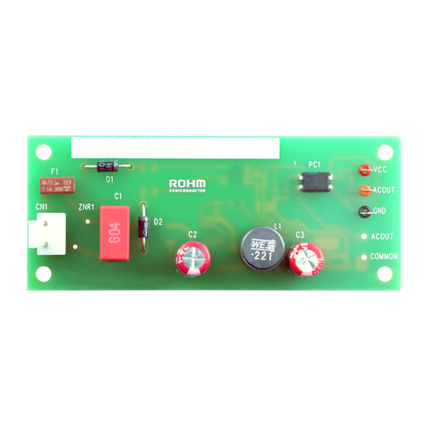
The BM2P141X-EVK-001 evaluation board outputs 14 V voltage from the input of 90 Vac to 264 Vac. The output current supplies up
to 0.715 A. The BM2P141X which is PWM method DC/DC converter IC built-in 650 V MOSFET is used.
The BM2P141X contributes to low power consumption by built-in a 650 V starting circuit. Built-in current detection resistor realizes
compact power supply design. Current mode control imposes current limitation on every cycle, providing superior performance in
bandwidth and transient response. The switching frequency is 65 kHz in fixed mode. At light load, frequency is reduced and high
efficiency is realized. Built-in frequency hopping function contributes to low EMI. Low on-resistance 1.5 Ω 650 V MOSFET built-in
contributes to low power consumption and easy design.
Figure 1. BM2P141X-EVK-001
Electronics Characteristics
Not guarantee the characteristics, is representative value.
Unless otherwise noted :VIN = 230 Vac, IOUT = 0.5 A, Ta:25 °C
(NOTE1) Please adjust operating time, within any parts surface temperature under 105 °C
(NOTE2) Not include spike noise
Parameter
Min
Typ
Max
Units
Conditions
Input Voltage Range
90
230
264
Vac
Input Frequency
47
50/60
63
Hz
Output Voltage
12.6
14.0
15.4
V
Maximum Output Power
-
-
10.0
W
IOUT = 0.715 A
Output Current Range
(NOTE1)
0.000
0.500
0.715
A
Stand-by Power
-
150
-
mW
IOUT = 0 A
Efficiency
80.0
83.7
-
%
Output Ripple Voltage
(NOTE2)
-
76
-
mVpp
Operating Temperature Range
-10
+25
+65
°C
2/20
© 2019 ROHM Co., Ltd.
No. 61UG024E Rev.002
Jul. 2021
User’s Guide
BM2P141X-EVK-001
Operation Procedure
1. Operation Equipment
(1) AC Power supply 90 Vac~264 Vac, over 20W
(2) Electronic Load capacity 0.715 A
(3) Multi meter
2. Connect method
(1) AC power supply presetting range 90~264 Vac, Output switch is off.
(2) Load setting under 0.715 A. Load switch is off.
(3) AC power supply N terminal connect to the boardAC (N) of CN1, and L terminal connect toAC(L).
(4) Load + terminal connect to VOUT, GND terminal connect to GND terminal
(5) AC power meter connect between AC power supply and board.
(6) Output test equipment connects to output terminal
(7) AC power supply switch ON.
(8) Check that output voltage is 14 V.
(9) Electronic load switch ON
(10) Check output voltage drop by load connect wire resistance
Figure 2. Connection Circuit
Deleting
Maximum Output Power Po of this reference board is 10.0 W. The derating curve is shown on the right. If ambient temperature
is over 40°C, Please adjust load continuous time by over 105 °C of any parts surface temperature.
Figure 3. Temperature Deleting curve
0
2
4
6
8
10
12
-25 0 25 50 75 100
Output Power Po [W]
Ambient Temparature Ta [℃]
AC
Power
Supply
DC Multi Meter
V
Electronics
Load
Power
Meter
CN1 : from the top ①:AC (L), ②:AC (N)
3/20
© 2019 ROHM Co., Ltd.
No. 61UG024E Rev.002
Jul. 2021
User’s Guide
BM2P141X-EVK-001
Application Circuit
VIN = 90 ~ 264 Vac, VOUT = 14 V
Figure 4. BM2P141X-EVK-001 Application Circuit
The BM2P141X is non-insulation method without opto-coupler and feeds back the VCC voltage to 14.0 V typ. This VCC voltage is the
voltage between the VCC pin and the GND_IC pin.
The output voltage VOUT is defined by the following equation.
   
VCNT: VCC Control Voltage
VFD1: Forward Voltage of diode D1
VFD2: Forward Voltage of diode D2
Figure 5. General Buck converter application circuit
Compared to the general Buck converter as shown above, the number of parts is reduced because the feedback circuit is not
required. However, the output voltage may rise at light load because the VCC voltage and the output voltage that are fed back are
different. In that case, please put a resistance on the output terminal and lower the output voltage.
VCC
1
N.C
N.C.
DRAIN
N.C.
GND_IC
N.C.
N.C.
2
3
4
8
7
6
5
GND
VOUT
IC
L
N
AC90-264V
D1
D2
GND
L
N
VCC
5
DRAIN
DRAIN
FB
GND
SOURCE
6
7
4
3
2
1
__
VOUT
AC90-264V
4/20
© 2019 ROHM Co., Ltd.
No. 61UG024E Rev.002
Jul. 2021
User’s Guide
BM2P141X-EVK-001
BM2P141X Overview
Feature
PWM Frequency=65 kHz
PWM current mode control
Switching frequency jitter
Burst function around light load
650 V Starter
650 V Super-Junction Power MOSFET
VCC Under voltage detection
VCC Over voltage detection
Cycle by cycle current limiter
Soft Start function
Key specifications
Operation Voltage Range: VCC: 12.00 V ~ 15.12 V
DRAIN 650 V(Max)
Circuit Current(ON): 0.85 mA(Typ)
Circuit Current (Burst mode): 0.45 mA(Typ)
Switching Frequency: 65 kHz(Typ)
Operating Temperature: -40 °C ~ +105 °C
MOSFET R-ON: 1.5 Ω(Typ)
Dimension W(Typ) x D(Typ) x H(Max)
DIP7K 9.20 mm x 6.35 mm x 4.30 mm
Pitch 2.54 mm
Figure 6. Block Diagram Figure 7. DIP7K Package
Table 1. BM2P141X PIN description
No.
Name
I/O
Function
ESD Diode
VCC
GND
1
-
-
-
-
-
2
-
-
-
-
-
3
GND_IC
I/O
GND
✔
-
4
-
-
-
-
-
5
VCC
I
Vcc
-
✔
6
DRAIN
I/O
MOSEFET DRAIN
-
✔
7
DRAIN
I/O
MOSEFET DRAIN
-
✔
5/20
© 2019 ROHM Co., Ltd.
No. 61UG024E Rev.002
Jul. 2021
User’s Guide
BM2P141X-EVK-001
Design Overview
1 Important parameter
VIN : Input Voltage Range AC 90 V ~ 264 Vac (DC 100 V ~ 380 V)
VOUT : Output Voltage DC 14 V
IOUT(Typ) : Constant Output Current 0.5 A
IOUT(Max) : Maximum Output Current 0.715 A
fSW : Switching Frequency Min:60 kHz, Typ:65 kHz, Max:70 kHz
Ipeak(Min) : Over Current Detection Current Min:1.8 A, Typ:2.0 A, Max:2.2A
2 Coil Selection
2.1 Determining Coil Inductance
The switching operation mode determines the L value so that it becomes as discontinuous mode (DCM) as possible. In the
continuous mode (CCM), reverse current in trr of the diode flows, which leads to an increase in power loss of diode.
Furthermore, this reverse current becomes the peak current when the MOSFET is ON, and the power loss of the MOSFET also
increases. The constant load current IOUT (Typ): 0.5 A, the peak current ILflowing through the inductor is:
 󰇛󰇜   [A]
It tends to be in continuous mode (CCM) when the input voltage drops.
Calculate with input voltage minimum voltage 100 Vdc
with 20% margin and VIN (Min) = 80 Vdc.
From the output voltage VOUT: 14 V and the diode VF: 1 V,
Calculate the maximum value of Duty: Duty (Max).
󰇛󰇜 
󰇛󰇜
Figure 8. Coil current waveform at OCP detection
From the minimum switching frequency fSW (Min) = 60 kHz,
Calculate on time ton (Max)
󰇛󰇜󰇛󰇜
󰇛󰇜  [μsec]
Calculate L value to operate in discontinuous mode.
  󰇛󰇜󰇛󰇜
  [μH]
t
tON
Iomax
IL
IL
Ip
Ipeak
tdly
OCP Detection
Iripple
ΔIL
6/20
© 2019 ROHM Co., Ltd.
No. 61UG024E Rev.002
Jul. 2021
User’s Guide
BM2P141X-EVK-001
2.1 Determining Coil Inductance –Continued
Also, calculate L value so that the overcurrent detection becomes maximum load current IOUT: 715 mA or more. Overcurrent
detection is calculated by the current flowing through the MOSFET when operating in continuous mode at the minimum
switching frequency fSW (Min) = 60 kHz. When the current flowing through the MOSFET (≠ the coil current at switching ON)
exceeds the minimum value Ipeak (Min): 1.8 A of the overcurrent detection current, the MOSFET is turned OFF. Since a delay
of approximately tdly = 0.1 μsec occurs, in reality, the peak current exceeds the Ipeak value and the peak current becomes Ip.
The peak current Ip is obtained by setting the current slope at switching ON to ΔIL,
 
  

Calculate the output current Io (LIM) at overcurrent detection by securing a margin of 10% from the maximum load current of
715 mA, and setting it as 787 mA.
󰇛󰇜
 󰇛󰇜
Calculate the minimum value of the L value of the coil. From the above formula,
  󰇝󰇛󰇜󰇛󰇜󰇛󰇜󰇞󰇛󰇛󰇜󰇜
󰇛󰇜󰇛󰇜󰇛󰇜󰇛󰇜 [μH]
Therefore, the inductance value of the coil is discontinuous mode when the rated current Io (Typ) is 0.5 A, and in order to detect
the overcurrent of the maximum load current Io (Max): 0.715 A or more, the condition of 95.0 μH to 206.3 μH , A coil of 150 μH
is selected.
2.2 Inductor Current Calculation
Calculate the maximum peak current of the inductor. The condition where the peak current is maximized is when the input
voltage is the maximum voltage VIN (Max): 380 V, the maximum load current Io (Max): 0.715 A, and the switching frequency is
60 kHz at the minimum.The ripple current Iripple of the coil is given by the following formula.
  
 󰇝󰇛󰇜󰇛 󰇜󰇞
󰇛 󰇜
󰇛󰇜󰇛󰇜
7/20
© 2019 ROHM Co., Ltd.
No. 61UG024E Rev.002
Jul. 2021
User’s Guide
BM2P141X-EVK-001
2.2 Inductor Current Calculation -Continued
When it is applied to the formula of the peak current,
 󰇛󰇜
 󰇝󰇛󰇜󰇛󰇜󰇞󰇛󰇜
󰇛󰇜󰇛󰇜 [A]
Select a coil with an allowable current of 1.52 A or more.
In this EVK, we use inductance value: 150 μH, rated: 1.9 A product.
Radial inductor (closed magnetic circuit type) Core size DR09 x 11 series
Product: XF1501Y-151
Manufacturer: ALPHA TRANS CO,. LTD
〒541-0059 Senbanishi KID Bldg 7F, 4-4-11, Bakurou-machi, Chuo-ku, Osaka
http://www.alphatrans.jp/
3 Diode Selection
3.1 Flywheel Diode : D1
Flywheel diode uses fast diode (fast recovery diode).The reverse voltage of the diode is VIN (Max): 380 V when the output
voltage at startup is 0 V. Consider the derating and select 600 V diode. The condition where the effective current of the diode is
maximized is when the input voltage is the maximum voltage VIN (Max): 380 V, the maximum load current Io (Max): 0.715 A,
and the switching frequency is 60 kHz at the minimum.
  
󰇛󰇜  [%]
The average current ID of the diode is calculated from the peak current Ip: 1.52 A by the following formula
󰇛󰇜
  [A]
Select the rated current of 0.860 A or more.
In fact, we used RFN5BM6S of 5 A / 600 V product as a result of mounting the board and considering the parts temperature.
3.2 VCC Rectifier Diode : D1
Rectifier diodes are used for diodes to supply VCC. The reverse voltage applied to the diode is VIN (Max): 380 V. Consider the
derating and select 600 V diode. Because the current flowing to the IC is small enough, we use the 0.2 A / 600 V
RRE02VSM6S.
8/20
© 2019 ROHM Co., Ltd.
No. 61UG024E Rev.002
Jul. 2021
User’s Guide
BM2P141X-EVK-001
Design Overview –Continued
4 Capacitor Selection
4.1 Input Capacitor : C4
The input capacitor is determined by input voltage VI and output power POUT. As a guide, for an input voltage of 90 to 264 Vac,
2 x POUT [W] μF. For 176 to 264 Vac, set 1 x POUT [W] μF. Since the output power POUT = 10 W, 22 μF / 450 V is selected at 20
μF or more.
4.2 VCC Capacitor : C6
The VCC capacitor CVCC is required for stable operation of the device and stable feedback of the output voltage. A withstand
voltage of 25 V or more is required, and 1.0 μF to 4.7 μF is recommended. 2.2 μF / 50 V is selected.
4.3 Output Capacitor : C7, C8
For the output capacitor, select output voltage VOof 25 V or more in consideration of derating. For C7 electrolytic capacitors,
capacitance, impedance and rated ripple current must be taken into consideration.
The output ripple voltage is a composite waveform generated by electrostatic capacity: Cout, impedance: ESR when the ripple
component of inductor current: ΔILflows into the output capacitor and is expressed by the following formula.
   

The inductor ripple current,
 󰇝󰇛󰇜󰇞 󰇛󰇜  [A]
For this EVK, we use electrostatic capacity: 680 μF, ESR: 0.049 Ω, and the design value of output ripple voltage is less than
100 mV.
  󰇥󰇡 
󰇢󰇦  󰇥󰇡 
󰇢󰇦   [mV]
Next, check whether the ripple current of the capacitor satisfies the rated ripple current.
Inductor ripple current RMS conversion,
󰇟󰇠 
 [A]
The ripple current of the capacitor,
󰇟󰇠  [A]
9/20
© 2019 ROHM Co., Ltd.
No. 61UG024E Rev.002
Jul. 2021
User’s Guide
BM2P141X-EVK-001
4.3 Output Capacitor C7, C8 –Continued
Select a rated current of 0.59A or more.
The output capacitor C7 used a rated ripple current of 1.24 A at 680 μF / 25 V.
C8 has added a 0.1 μF ceramic capacitor to reduce switching noise.
5 Resistor Selection
5.1 Discharge Resistor : R1,R2,R3
The resistor is for discharging X - Capacitor (C1). Considering withstand voltage, 3 pcs of chip resistance of ROHM
product MCR18 (200 V withstand voltage) are connected in series. 220 kΩ is used in 3 pcs in series so that it becomes 45
V or less after 1 second after turning off the power supply.
5.2 Bleeder Resister : R4
Because it is indirectly fed back to the output voltage, the output voltage increases at light load. This board uses bleeder
resistance for its improvement. Reducing the resistance value improves the rise in the output voltage of the light load, but
increases the power loss. 10 kΩ / 0.25 W is used.
6 EMI Filter Selection
As a measure against "Conducted Emission", Input filter is composed of X-Capacitor: C1 and common mode filter LF1.
X-Capacitor uses 0.22 μF / X 2. The common mode filter uses 13 mH (Min) / 1 A.
As a measure against "Radiated Emission", Input filter is composed of Y-Capacitor: C2, C3 and a common mode filter LF2.
Y - Capacitor uses 2200 pF / Y1 and connects the midpoint to the output capacitor so that high frequency noise is not
propagated from the input. Moreover, the common mode filter uses 60 μH (Min) / 1 A with good characteristics of the 100
MHz band. If "Radiated Emission" does not have a problem in the state that it is loaded in the set, C2, C3, LF2 are
unnecessary.
10/20
© 2019 ROHM Co., Ltd.
No. 61UG024E Rev.002
Jul. 2021
User’s Guide
BM2P141X-EVK-001
Performance Data
Constant Load Regulation
Figure 8. Load Regulation (IOUT vs. VOUT) Figure 9. Load Regulation (IOUT vs. Efficiency)
Table 2. Load Regulation (VIN=115 Vac) Table 3. Load Regulation (VIN=230 Vac)
IOUT
VOUT
Efficiency
IOUT
VOUT
Efficiency
179 mA
13.737 V
84.64 %
179 mA
13.720 V
80.47 %
358 mA
13.705 V
85.45 %
358 mA
13.687 V
82.52 %
536 mA
13.690 V
85.77 %
536 mA
13.674 V
83.48 %
715 mA
13.681 V
83.36 %
715 mA
13.665 V
84.01 %
Figure 10. Load Regulation (IOUT vs. PLOSS) Figure 11. Load Regulation (IOUT vs. PLOSS)
12.6
12.8
13.0
13.2
13.4
13.6
13.8
14.0
14.2
14.4
14.6
14.8
15.0
15.2
15.4
0 500 1000 1500
Output Voltage [V]
Output Current [mA]
-VIN= 90 Vac
-VIN=230 Vac
-VIN=115 Vac
-VIN=264 Vac
0
10
20
30
40
50
60
70
80
90
100
0 100 200 300 400 500 600 700
Efficiency [%]
Output Current [mA]
-VIN=90 Vac
-VIN=230 Vac
-VIN=115 Vac
-VIN=264 Vac
0.0
0.5
1.0
1.5
2.0
2.5
0 100 200 300 400 500 600 700
Power Loss [W]
Output Current [mA]
-VIN= 90 Vac
-VIN=230 Vac
-VIN=115 Vac
-VIN=264 Vac
0.0
0.1
0.2
0.3
0.4
0.5
110 100
Power Loss [W]
Output Current [mA]
-VIN= 90 Vac
-VIN=230 Vac
-VIN=115 Vac
-VIN=264 Vac
11/20
© 2019 ROHM Co., Ltd.
No. 61UG024E Rev.002
Jul. 2021
User’s Guide
BM2P141X-EVK-001
Performance Data -Continued
Table 4. Load Regulation : VIN=90 Vac Table 5. Load Regulation: VIN=100 Vac
Table 6. Load Regulation: VIN=115 Vac Table 7. Load Regulation: VIN=176 Vac
VIN
[Vac]
PIN
[W]
VOUT
[V]
IOUT
[mA]
POUT
[W]
PLOSS
[W]
Efficiency
[%]
90 0.05 14.459 0 0.000 0.051 0.00
90 0.06 14.352 1 0.014 0.048 23.15
90 0.08 14.279 2 0.029 0.046 38.08
90 0.12 14.164 5 0.071 0.052 57.58
90 0.16 14.132 7 0.099 0.058 63.01
90 0.21 14.106 10 0.141 0.068 67.49
90 0.29 14.077 15 0.211 0.083 71.82
90 0.38 14.059 20 0.281 0.096 74.58
90 0.53 13.968 30 0.419 0.115 78.47
90 0.85 13.883 50 0.694 0.153 81.95
90 1.16 13.833 70 0.968 0.194 83.33
90 1.63 13.784 100 1.378 0.256 84.36
90 2.89 13.740 179 2.459 0.429 85.16
90 3.22 13.736 200 2.747 0.474 85.29
90 4.81 13.717 300 4.115 0.693 85.59
90 5.73 13.710 358 4.908 0.821 85.67
90 7.98 13.697 500 6.849 1.132 85.82
90 8.55 13.696 536 7.341 1.210 85.85
90 11.45 13.685 715 9.785 1.664 85.46
90 12.85 13.681 800 10.945 1.909 85.15
90 16.17 13.665 1000 13.665 2.509 84.49
90 19.57 13.651 1200 16.381 3.184 83.73
90 20.26 13.625 1240 16.895 3.361 83.41
90 0.07 0.000 1250 0.000 0.070 0.00
VIN
[Vac]
PIN
[W]
VOUT
[V]
IOUT
[mA]
POUT
[W]
PLOSS
[W]
Efficiency
[%]
100 0.05 14.537 0 0.000 0.054 0.00
100 0.07 14.406 1 0.014 0.052 21.83
100 0.08 14.317 2 0.029 0.050 36.25
100 0.13 14.181 5 0.071 0.055 56.27
100 0.16 14.142 7 0.099 0.061 61.87
100 0.21 14.114 10 0.141 0.072 66.26
100 0.30 14.085 15 0.211 0.087 70.90
100 0.38 14.064 20 0.281 0.101 73.63
100 0.54 13.982 30 0.419 0.122 77.53
100 0.85 13.888 50 0.694 0.160 81.31
100 1.17 13.837 70 0.969 0.199 82.93
100 1.64 13.787 100 1.379 0.261 84.07
100 2.89 13.738 179 2.459 0.434 85.00
100 3.23 13.733 200 2.747 0.478 85.17
100 4.81 13.713 300 4.114 0.696 85.53
100 5.73 13.707 358 4.907 0.823 85.64
100 7.98 13.694 500 6.847 1.129 85.85
100 8.55 13.693 536 7.339 1.206 85.89
100 11.45 13.682 715 9.783 1.662 85.48
100 12.86 13.679 800 10.943 1.914 85.11
100 16.17 13.663 1000 13.663 2.511 84.48
100 19.55 13.649 1200 16.379 3.167 83.80
100 20.37 13.630 1250 17.038 3.330 83.65
100 0.08 0.000 1260 0.000 0.080 0.00
VIN
[Vac]
PIN
[W]
VOUT
[V]
IOUT
[mA]
POUT
[W]
PLOSS
[W]
Efficiency
[%]
115 0.06 14.611 0 0.000 0.062 0.00
115 0.07 14.458 1 0.014 0.059 19.81
115 0.09 14.354 2 0.029 0.057 33.38
115 0.13 14.197 5 0.071 0.062 53.37
115 0.17 14.151 7 0.099 0.068 59.32
115 0.22 14.114 10 0.141 0.077 64.74
115 0.30 14.088 15 0.211 0.093 69.51
115 0.39 14.067 20 0.281 0.110 71.95
115 0.55 14.005 30 0.420 0.133 75.98
115 0.87 13.896 50 0.695 0.171 80.23
115 1.18 13.842 70 0.969 0.211 82.11
115 1.65 13.789 100 1.379 0.273 83.47
115 2.91 13.737 179 2.459 0.446 84.64
115 3.24 13.732 200 2.746 0.492 84.82
115 4.82 13.712 300 4.114 0.710 85.27
115 5.74 13.705 358 4.906 0.836 85.45
115 7.99 13.691 500 6.846 1.142 85.71
115 8.56 13.690 536 7.338 1.217 85.77
115 11.46 13.681 715 9.782 1.678 85.36
115 12.88 13.677 800 10.942 1.942 84.92
115 16.22 13.662 1000 13.662 2.555 84.24
115 19.59 13.647 1200 16.376 3.211 83.61
115 20.65 13.641 1260 17.188 3.462 83.23
115 0.09 0.000 1270 0.000 0.090 0.00
VIN
[Vac]
PIN
[W]
VOUT
[V]
IOUT
[mA]
POUT
[W]
PLOSS
[W]
Efficiency
[%]
176 0.10 14.803 0 0.000 0.101 0.00
176 0.11 14.601 1 0.015 0.096 13.15
176 0.13 14.457 2 0.029 0.096 23.13
176 0.17 14.238 5 0.071 0.101 41.39
176 0.21 14.170 7 0.099 0.107 48.15
176 0.26 14.112 10 0.141 0.116 54.91
176 0.34 14.066 15 0.211 0.133 61.33
176 0.43 14.050 20 0.281 0.149 65.35
176 0.61 14.022 30 0.421 0.184 69.53
176 0.93 13.930 50 0.697 0.235 74.81
176 1.25 13.858 70 0.970 0.275 77.92
176 1.72 13.798 100 1.380 0.340 80.22
176 2.98 13.726 179 2.457 0.518 82.59
176 3.31 13.721 200 2.744 0.568 82.86
176 4.91 13.700 300 4.110 0.800 83.71
176 5.83 13.694 358 4.902 0.932 84.03
176 8.09 13.682 500 6.841 1.249 84.56
176 8.66 13.682 536 7.334 1.328 84.66
176 11.56 13.675 715 9.778 1.780 84.60
176 13.08 13.675 800 10.940 2.140 83.64
176 16.56 13.662 1000 13.662 2.901 82.49
176 20.06 13.648 1200 16.378 3.679 81.66
176 22.50 13.609 1330 18.100 4.398 80.45
176 0.17 0.000 1340 0.000 0.172 0.00
12/20
© 2019 ROHM Co., Ltd.
No. 61UG024E Rev.002
Jul. 2021
User’s Guide
BM2P141X-EVK-001
Performance Data -Continued
Table 8. Load Regulation : VIN=230 Vac Table 9. Load Regulation: VIN=264 Vac
VIN
[Vac]
PIN
[W]
VOUT
[V]
IOUT
[mA]
POUT
[W]
PLOSS
[W]
Efficiency
[%]
230 0.15 15.041 0 0.000 0.148 0.00
230 0.16 14.764 1 0.015 0.143 9.34
230 0.17 14.577 2 0.029 0.143 16.95
230 0.22 14.292 5 0.071 0.148 32.63
230 0.25 14.204 7 0.099 0.155 39.14
230 0.30 14.130 10 0.141 0.163 46.48
230 0.39 14.069 15 0.211 0.180 53.97
230 0.48 14.038 20 0.281 0.202 58.13
230 0.66 14.015 30 0.420 0.237 64.00
230 1.01 13.985 50 0.699 0.307 69.51
230 1.32 13.884 70 0.972 0.351 73.46
230 1.80 13.811 100 1.381 0.417 76.81
230 3.05 13.720 179 2.456 0.596 80.47
230 3.39 13.714 200 2.743 0.648 80.88
230 5.00 13.693 300 4.108 0.896 82.09
230 5.94 13.687 358 4.900 1.038 82.52
230 8.21 13.673 500 6.837 1.374 83.27
230 8.78 13.674 536 7.329 1.451 83.48
230 11.63 13.665 715 9.770 1.860 84.01
230 13.23 13.663 800 10.930 2.300 82.62
230 16.83 13.646 1000 13.646 3.184 81.08
230 20.47 13.638 1200 16.366 4.104 79.95
230 24.02 13.583 1390 18.880 5.140 78.60
230 0.25 0.000 1400 0.000 0.250 0.00
VIN
[Vac]
PIN
[W]
VOUT
[V]
IOUT
[mA]
POUT
[W]
PLOSS
[W]
Efficiency
[%]
264 0.19 15.109 0 0.000 0.186 0.00
264 0.20 14.835 1 0.015 0.180 7.61
264 0.21 14.635 2 0.029 0.179 14.07
264 0.26 14.320 5 0.072 0.184 27.97
264 0.29 14.222 7 0.100 0.190 34.33
264 0.34 14.140 10 0.141 0.201 41.35
264 0.43 14.065 15 0.211 0.216 49.41
264 0.52 14.032 20 0.281 0.234 54.49
264 0.69 14.006 30 0.420 0.273 60.63
264 1.05 13.969 50 0.698 0.352 66.52
264 1.38 13.909 70 0.974 0.407 70.50
264 1.86 13.820 100 1.382 0.475 74.42
264 3.11 13.720 179 2.456 0.657 78.89
264 3.45 13.709 200 2.742 0.708 79.47
264 5.07 13.687 300 4.106 0.965 80.97
264 6.01 13.681 358 4.898 1.110 81.52
264 8.29 13.669 500 6.835 1.456 82.44
264 8.87 13.669 536 7.327 1.543 82.60
264 11.72 13.660 715 9.767 1.953 83.34
264 13.32 13.660 800 10.928 2.392 82.04
264 16.92 13.624 1000 13.624 3.296 80.52
264 20.57 13.607 1200 16.328 4.242 79.38
264 23.95 13.520 1400 18.928 5.022 79.03
264 0.30 0.000 1410 0.000 0.300 0.00
13/20
© 2019 ROHM Co., Ltd.
No. 61UG024E Rev.002
Jul. 2021
User’s Guide
BM2P141X-EVK-001
Performance Data -Continued
Line Regulation
Figure 12. Line Regulation (IIN vs. VOUT) Figure 13. Line Regulation (IIN vs. Efficiency)
Figure 14. Switching Frequency (IOUT vs. FSW) Figure 15. Coil Peak Current (IOUT vs. Ipeak)
12.6
12.8
13.0
13.2
13.4
13.6
13.8
14.0
14.2
14.4
14.6
14.8
15.0
15.2
15.4
80 100 120 140 160 180 200 220 240 260 280
Output Voltage [V]
Input Voltage [Vac]
-IOUT= 10 mA
-IOUT=100 mA
-IOUT=500 mA
-I
OUT
=715 mA
0
10
20
30
40
50
60
70
80
90
100
80 100 120 140 160 180 200 220 240 260 280
Efficiency [%]
Input Voltage [Vac]
-IOUT= 10 mA
-IOUT=100 mA
-IOUT=500 mA
-I
OUT
=715 mA
0
10
20
30
40
50
60
70
0 100 200 300 400 500 600 700 800
Switching Frequency [kHz]
Output Current [mA]
-VIN=115 Vac
-VIN=230 Vac
0.0
0.2
0.4
0.6
0.8
1.0
1.2
1.4
1.6
1.8
2.0
0 100 200 300 400 500 600 700 800
Coil Peak Current [A]
Output Current [mA]
-VIN=115 Vac
-VIN=230 Vac
14/20
© 2019 ROHM Co., Ltd.
No. 61UG024E Rev.002
Jul. 2021
User’s Guide
BM2P141X-EVK-001
Performance Data -Continued
Operation Waveform
Figure 16. MOSFET VIN = 90 Vac, IOUT = 0.715 A Figure 17. Diode VIN = 90 Vac, IOUT=0.715 A
Figure 18. MOSFET VIN = 264 Vac, IOUT = 0.715 A Figure 19. Diode VIN = 264 Vac, IOUT = 0.715 A
Figure 20. MOSFET VIN = 264 Vac, Output Short Figure 21. Diode VIN = 264 Vac, Output Short
MOSFET VDS
MOSFET IDrain
Diode IF
Diode VAnode-Cathode
Diode IF
Diode VAnode-Cathode
MOSFET VDS
MOSFET IDrain
Diode IF
Diode VAnode-Cathode
MOSFET VDS
MOSFET
IDrain
15/20
© 2019 ROHM Co., Ltd.
No. 61UG024E Rev.002
Jul. 2021
User’s Guide
BM2P141X-EVK-001
Performance Data -Continued
Power ON
Figure 22. VIN = 115 Vac, IOUT = 0.715 A Figure 23. VIN = 230 Vac, IOUT = 0.715 A
Dynamic Response
Figure 24. VIN = 115 Vac, IOUT = 10 mA → 0.715 A Figure 25. VIN = 115 Vac, IOUT = 0.715 A → 10 mA
Figure 26. VIN = 230 Vac, IOUT = 10 mA → 0.715 A Figure 27. VIN = 230 Vac, IOUT = 0.715 A → 10 mA
VOUT
IOUT
VOUT
IOUT
VOUT
IOUT
VOUT
IOUT
16/20
© 2019 ROHM Co., Ltd.
No. 61UG024E Rev.002
Jul. 2021
User’s Guide
BM2P141X-EVK-001
Performance Data -Continued
Output Ripple Voltage
Figure 28. VIN = 115 Vac, IOUT = 10 mA Figure 29. VIN = 230 Vac, IOUT = 10 mA
Figure 30. VIN = 115 Vac, IOUT = 0.5 A Figure 31. VIN = 230 Vac, IOUT = 0.5 A
Figure 32. VIN = 115 Vac, IOUT = 0.715 A Figure 33. VIN = 230 Vac, IOUT = 0.715 A
VOUT
VOUT
VOUT
VOUT
VOUT
VOUT
17/20
© 2019 ROHM Co., Ltd.
No. 61UG024E Rev.002
Jul. 2021
User’s Guide
BM2P141X-EVK-001
Performance Data -Continued
Parts surface temperature
Table 10. Parts surface temperature Ta = 25 °C, measured 30minites after startup
Part
Condition
VIN = 90 Vac,
IOUT = 0.500 A
VIN = 90 Vac,
IOUT = 0.715 A
VIN = 264 Vac,
IOUT = 0.500 A
VIN = 264 Vac,
IOUT = 0.715 A
IC1
50.4 °C
67.3 °C
51.8 °C
64.9 °C
D1
61.5 °C
76.9 °C
64.3 °C
77.5 °C
DB1
49.6 °C
54.8 °C
44.1 °C
46.0 °C
L1
49.8 °C
61.8 °C
47.6 °C
62.5 °C
EMI
・Conducted Emission: CISPR22 Pub 22 Class B
Figure 34. VIN = 110 Vac / 60 Hz, IOUT = 0.715 A Figure 35. VIN = 230 Vac / 50 Hz, IOUT = 0.715 A
QP margin = 13.5 dB, AV margin = 20.5 dB QP margin = 18.3 dB, AV margin = 23.9 dB
・Radiated Emission: CISPR22 Pub 22 Class B
Figure 36. VIN = 110 Vac / 60 Hz, IOUT = 0.715 A Figure 37. VIN = 230 Vac / 50 Hz, IOUT = 0.715 A
QP margin = 6.6 dB QP margin = 6.0 dB
18/20
© 2019 ROHM Co., Ltd.
No. 61UG024E Rev.002
Jul. 2021
User’s Guide
BM2P141X-EVK-001
Schematics
VIN = 90~264 Vac, VOUT = 14 V
Figure 38. BM2P141X-EVK-001 Schematics
Bill of Materials
Table 11. BoM of BM2P141X-EVK-001
Part
Reference
Qty. Type Value Description Part Number Manufacture
Configuration
mm (inch)
C1 1 X2 Capacitor 0.22μF275Vac, ±20% 890324023028CS Wurth -
C2,C3 2 Y1 Capacitor 2200pF Y1 capacitor DE1E3KX222MB4BP01F Murata -
C4 1 Electrolytic 22μF450V, ±20% 450BXW22MEFR12.5X20 Rubycon 12.5mmΦX20mm
C5 1 Ceramic 100pF 1kV, C0G, ±10% GRM31A5C3A101J Murata 3216 (1206)
C6 1 Ceramic 2.2μF50V, X7R, ±10% UMK316B7225KL-T Taiyo Yuden 3216 (1206)
C7 1 Electrolytic 680uF 25V , ±20% UPA1E681MPD Nichicon 10mmΦX16mm
C8 1 Ceramic 0.1µF 100V, X7R, ±10% HMK107B7104MA-T Taiyo Yuden 1608 (0603)
CN1 1 Connector 2pin 5mm pitch B2P-NV JST -
D1 1 FRD 5A 600V RFN5BM6S ROHM TO-252
D2 1 REC Di 0.2A 600V RRE02VSM6S ROHM TUMD2SM
DB1 1 Bridge 1A 800V D1UBA80 Shindengen SOP-4
F1 1 Fuse 1.6A 1.6A 300V 36911600000 Littelfuse -
IC1 1 AC/DC Converter - 650V BM2P141X-Z ROHM DIP7
JP1 1 Jumper - Jumper Wire - - Φ0.5mm
L1 1 Coil 150μH 1.9A XF1501Y-151 Alpha Trans -
LF1 1 Line Filter 13mH 1A XF1482Y Alpha Trans -
LF2 1 Line Filter 60μH1A LF1246Y Alpha Trans -
PCB 1 FR4 - - - - -
R1,R2,R3 3 Resistor 220kΩ 0.25W, ±5% MCR18EZPJ224 ROHM 3216 (1206)
R4 1 Resistor 10kΩ 0.25W, ±5% MCR18EZPJ103 ROHM 3216 (1206)
ZNR1 1 Varistor - 300Vac, 423Vmin, 400A V470ZA05P Littelfuse 5mmΦ Disc

Other manuals for BM2P141X

1

This manual suits for next models

1

Other Rohm Motherboard manuals

Rohm Lapis Technology RB-D610Q327TB48 User manual

Rohm

Rohm Lapis Technology RB-D610Q327TB48 User manual

Rohm BM92A14MWV-EVK-001 User manual

Rohm

Rohm BM92A14MWV-EVK-001 User manual

Rohm BD7F105EFJ-EVK-001 User manual

Rohm

Rohm BD7F105EFJ-EVK-001 User manual

Rohm Shield-EVK-001 User manual

Rohm

Rohm Shield-EVK-001 User manual

Rohm KX132-1211-EVK-001 User manual

Rohm

Rohm KX132-1211-EVK-001 User manual

Rohm HB2637L-EVK-301 User manual

Rohm

Rohm HB2637L-EVK-301 User manual

Rohm BD71837MWV Guide

Rohm

Rohm BD71837MWV Guide

Rohm BM1Z002FJ User manual

Rohm

Rohm BM1Z002FJ User manual

Rohm BM92A56MWV-ZE2 User manual

Rohm

Rohm BM92A56MWV-ZE2 User manual

Rohm BM1Z002FJ User manual

Rohm

Rohm BM1Z002FJ User manual

Rohm BD9E201FP4-Z User manual

Rohm

Rohm BD9E201FP4-Z User manual

Rohm BU94603 User manual

Rohm

Rohm BU94603 User manual

Rohm BD63 EFV-EKV-001 Series User manual

Rohm

Rohm BD63 EFV-EKV-001 Series User manual

Rohm BM92A56MWV-EVK-001 Quick start guide

Rohm

Rohm BM92A56MWV-EVK-001 Quick start guide

Rohm BM2P060MF-EVK-001 User manual

Rohm

Rohm BM2P060MF-EVK-001 User manual

Rohm BD7F100EFJ-EVK-002 User manual

Rohm

Rohm BD7F100EFJ-EVK-002 User manual

Rohm BM3G007MUV-EVK-003 User manual

Rohm

Rohm BM3G007MUV-EVK-003 User manual

Rohm SENSEKIT1-EVK-101 User manual

Rohm

Rohm SENSEKIT1-EVK-101 User manual

Rohm BD63800MUF-EVK-002 User manual

Rohm

Rohm BD63800MUF-EVK-002 User manual

Rohm BD868 0MUF-C Series User manual

Rohm

Rohm BD868 0MUF-C Series User manual

Rohm TO-247N User manual

Rohm

Rohm TO-247N User manual

Rohm BM1Z102FJ User manual

Rohm

Rohm BM1Z102FJ User manual

Rohm Lapis MK715 1 Evaluation Kit Mini Plus... User manual

Rohm

Rohm Lapis MK715 1 Evaluation Kit Mini Plus... User manual

Rohm BM1383AGLV-EVK-001 User manual

Rohm

Rohm BM1383AGLV-EVK-001 User manual

Popular Motherboard manuals by other brands

ASROCK Fatality H97 Killer series user manual

ASROCK

ASROCK Fatality H97 Killer series user manual

ASROCK H55M R2.0 user manual

ASROCK

ASROCK H55M R2.0 user manual

CompuLab SBC-FITPC2 reference guide

CompuLab

CompuLab SBC-FITPC2 reference guide

Gigabyte GA-MA78GM-S2H user guide

Gigabyte

Gigabyte GA-MA78GM-S2H user guide

Gigabyte GA-8N-SLI Royal user manual

Gigabyte

Gigabyte GA-8N-SLI Royal user manual

Asus P5N-VM WS - Motherboard - Micro ATX manual

Asus

Asus P5N-VM WS - Motherboard - Micro ATX manual

Asus M2NBP-VM CSM user guide

Asus

Asus M2NBP-VM CSM user guide

MSI X370 GAMING PLUS manual

MSI

MSI X370 GAMING PLUS manual

Dialog Semiconductor DA9155M user manual

Dialog Semiconductor

Dialog Semiconductor DA9155M user manual

OLIMEX LPC-E2468 user manual

OLIMEX

OLIMEX LPC-E2468 user manual

Wiznet WIZ-iRadio user manual

Wiznet

Wiznet WIZ-iRadio user manual

Supero X9SCE-F user manual

Supero

Supero X9SCE-F user manual

Taiwan Commate Computer Inc. 370SMA user manual

Taiwan Commate Computer Inc.

Taiwan Commate Computer Inc. 370SMA user manual

EPOX EP-D3VA user manual

EPOX

EPOX EP-D3VA user manual

Renesas RTKA211820DE0000BU manual

Renesas

Renesas RTKA211820DE0000BU manual

MACOM MAOM-37447 user guide

MACOM

MACOM MAOM-37447 user guide

ADLINK Technology cExpress-AL user manual

ADLINK Technology

ADLINK Technology cExpress-AL user manual

Apex Digital MSA240KC manual

Apex Digital

Apex Digital MSA240KC manual

manuals.online logo
manuals.online logoBrands
  • About & Mission
  • Contact us
  • Privacy Policy
  • Terms and Conditions

Copyright 2025 Manuals.Online. All Rights Reserved.