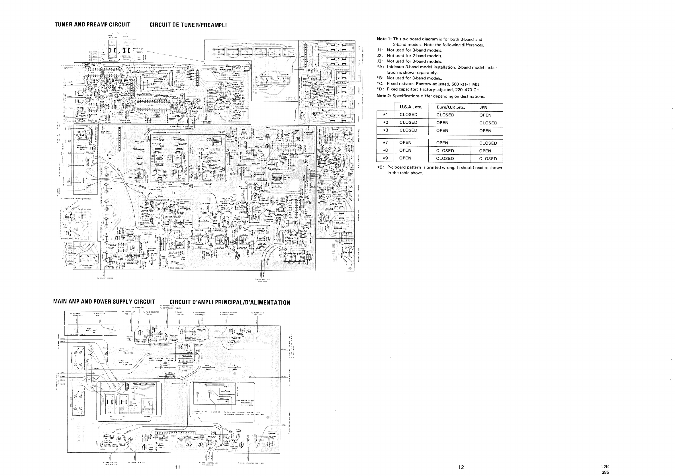
Rotel RX-700L User manual

Quality
Uncompromised.
ee
Technical
Manual
THE
ROTEL
CO.
LTP.
QUARTZ
PLL
SYNTHESIZER
AM/FM
STEREO
RECEIVER
RX-/OOZL
TABLE
OF
CONTENTS
Description
of
Function
2
ok
eee
Se
ee
ee
ee
ee
2
AMONIMEN
Cod
io
a
a
ee
Sh
OE SS
eS
We
3
Troubleshooting
Guide.
.......0.0.
0...
ee
ee
ee
eee
6
Paris
(hiSt.
fc
64
Gee
sos
Se
Ee
We
A
Re
Oe
7
Specifications
=...
oss.
BS
wR
AS
Sr
es
9
Chassis
Layout
(Top
View)
..........
00002
ee
eae
10
BIGCK:
Diagrannte.
esc:
4
Soccer:
oe
ewe
Gea
eer
Ke
eS
10
Circuit
Board:
Disgranse
«0606.
8 6
4.
BABS
6
Se
oe
GOA
eS
11
Schematic
Diagram
=
2.6
2
6.8
o
Dera
WR
ae
a
Bw
ow
ee
ews
13
TABLE
DES
MATIERES
Description
des
fonctions
........0.
200
pee
eee
eee
2
PUIGMEMENE
:6:
Aicd
Shi
Gi
eee
Se
ee
WG
eee
a
we
Be
ew
3
Guide
de
dépannage
..........0
0.
eee eee
eee
ae
6
PISte
CO°DIOCES
so
ca
5
oe
gx
wb
d
Soe
eed
Se
oe
ee
7
CaracteriStiQues:
2.10
ce
ws
dab
bed,
SS
We
wa
BS
aR
OO
9
Installation
du
chassis
(vue
de
dessus)
...........00..
10
Schémasynoptique.
.......
2.0.
eee
ee
es
10
Diagrammes
des
plaquettes
des
circuits
imprimés.
.......
11
Diagramme
schématique...........
02
e
ee
ene
es
erm
|
Serial
Nos.
Beginning
NE16261
1-36-8
OHOKAY
AMA,
MEGURO-KU,
TOKYO
152,
JAPAN
2ND
FLOOR,
EVERGLORY
BLDG.,
NO.
305,
SECTION
3
ROTEL
ELECTRONICS
CO.,,
LTD.
Nanking
€’
ROAD,
TAIPEI,
TAIWAN,
REPUBLIC
OF
CHINA
ROTELW
OF
AMERICA,
INC.
ROTTEN
HIF!
LIMITED.
13528
SO.
NORMANDIE,
GARDENA,
CALIF.
90249,
U.S.A.
2-4
ERICA
ROAD,
STACEY
BUSHES,
MILTON
KEYNES,
BUCKINGHAMSHIRE,
ENGLAND

DESCRIPTION
OF
FUNCTION
1.
Memory
a)
Preset
stations:
5
FM
stations
plus
5
AM
(LW/MW)
stations
(10
stations
in
total).
b)
Last
channel:
1
station
for
each
band.
2.
Memory
backup:
Battery
backup
method
(about
one
year).
3.
Automatic
tuning
is
possible
only
for
FM
band.
4.
Receiving
frequency
ranges,
etc.
are
shown
in
the
DESCRIPTION
DES
FONCTIONS
1.
Mémoire
a}
Stations
préréglées:
5
stations
MF
et
5
stations
MA
(GO/OM)
(10
stations
au
total)
b)
Dernier
canal:
1
station
dans
chaque
gamme.
2.
Renfort
de
mémoire:
Piles
d
e
secours
(environ
un
an).
3.
L’accord
par
auto-exploration
n‘est
possible
que
dans
la
gamme
MF.
4.
Les
gammes
de
fréquences
recues,
etc,
sont
indi-
table
below.
Table
1
Tableau
1
queées
au
tableau
ci-aprés.
Area
Band
Frequency
Range
Channel
Space
ae
IF
Région
Gamme
Fréquence
|
shai
:
stall
FI
Mw
530kHz
—
1620kHz
10kHz
10kHz
A50kHz
USA
(
MW2
522kHz
—
1611kHz
9kHz
—
QOkHz
450kHz
)
FM
87.9MHz
—
107.9MHz
200kHz
25kHz
10.70MHz
MW
522kHz
—
1611kHz
9kHz
|
kHz
450kHz
Europe,
UK,
etc.’
LW
146kHz
—
353kHz
9kHz
1kHz
|
450kHz
FM
87.50MHz
—
108.0MHz
50kHz
25kHz
10.70MHz
Note:
Units
for
the
U.S.A.
are
preset
for
MW1
(channel
space
=
10kHz).
9.
The
following
tables
show
frequency
ranges,
etc.
for
respective
areas,
which
are
preset
by
opening
or
closing
certain
part
of
controller
circuit
or
tuner
circuit.
Table
2
a)
Presetting
FM
and
MW
Bands
USA
EUROPE
UK
Notes:
Note:
Les
appareils
pour
les
U.S.A.
sont
préréglés
en
MW1
(OM1)
(intervalle
entre
canaux
=
10kHz).
©.
Les
tableaux
suivants
indiquent
les
gammes
de
fré-
quence,
etc,
selon
les
zones
respectives,
qui
font
l'objet
d’un
réglage
par
ouverture
ou
fermeture
de
certaines
sections
du
circu
circuit
de
section
tuner.
Frequency
Range
Chan
it
de
commande
ou
du
Tableau
2
a)
Préréglages
dans
les
gammes
MF
et
OM
nel
Space
CLOSED
|
87.50MHz—108.00MHz
1.
FM
band
is
preset
by
combining
*7
and
*8
(it
cannot
be
preset
when
*7
and
*8
are
closed).
2.
MW
(*9)
can
be
preset
independent
of
FM
band.
3.
If
settings
for
*7,
*8
and
*9
are
changed
while
the
unit
is
operating,
PLL
data
and
display
do
not
change.
It
is
therefore
necessary
to
put
the
unit
in
the
standby
state
beforehand.
b
b
—
3°“
Presetting
FM
Muting
(Auto-stop)
Lock
Range
Préréglage
de
la
gamme
de
verrouillage
(arrét
auto-
matique)
de
silencieux
MF
Area
Lock
Range
*
1
Zone
Gamme
de
|
verrouillage
USA
CLOSED
CLOSED
+70kHz
EUROPE
CLOSED
OPEN
+30kHz
UK
Table
3.
Tableau
3
CLOSED
§22kHz—1611kHz
Notes:
1.
La
gamme
MF
est
préréglée
en
réglage
ne
peut
étre
opéré
lorsque
*7
et
*8
sont
fermés).
2.
La
gamme
OM
(*9)
peut
étre
préréglée
indépendamment
de
la
gamme
MF.
Lorsque
les
réglages
de
*7,
*8
et
*9
sont
modifiés
alors
que
l‘appareil
est
en
marche,
les
do
Espacement
des
Gamme
de
frequences
canaux
87.9MH2—107.9MHz
200kHz
530kH2z—1620kHz
10kHz
50kHz
9kHz
combinant
*7
et
*8
(le
pré-
nnées
PLL
et
l'affichage
ne
changent
pas.
II
est
donc
nécessaire
de
mettre
l'appareil
en
mode
d’attante
au
préalable.
c)
Presetting
FM
De-emphasis
c)
Préréglage
de
désaccentuatio
n
MF
*3
De-emphasis
Zone
Désaccentuation
75us
USA
CLOSED
EUROPE
OPEN
5Ous
UK
|
|
Table
4
Tableau
4

Alignment
Instruments:
FM
signal
generator,
FM
stereo
signal
gene-
rator,
AM
signal
generator,
oscilloscope,
HD
analyzer,
DC
digital
voltmeter,
AC
voltmeter,
zero-center
meter
@
Adjustment
should
be
made
in
the
following
order.
1)
FM
2)
MW
3)
LW
FM
ALIGNMENT
A.
VCO
Adjustment
1.
Connect
the
DC
voltmeter
to
kinky
pin
on
the
FM
OSC
section
and
chassis
ground.
Operate
the
scanning
button
to
display
the
lower
edge
frequency*!
on
the
frequency
display.
Then
adjust
FM
OSC
coil
L106
so
that
the
DC
voltmeter
reads
3V+0.5V.
2.
Then
display
the
higher
edge
frequency*?,
and
adjust
the
trimmer
capacitor
CT104
so
that
the
DC
volt-
meter
reads
19V+0.1V.
3.
Repeat
steps
1
and
2
until
no
further
improvement
is
noticed.
Note:
*!,
**:
Band
edge
varies
according
to
area,
as
shown
in
the
table.
Table
5
Tableau
5
lower
Edge
|
Higher
Edge
Channel
Space
Limite
infé-
|
Limité
supé-
Espacement
rieure
'
rieure
des
canaux
87.50MHz
108.00MHz
50kHz
EUROPE,
UK
107.9MHz
200kHz
B.
FMRF
Sensitivity
Adjustment
1.
Receive
SOMHz
(90.1MHz,
channel
space
=
200
kHz)
signal
from
the
FM
signal
generator.
Adjust
the
FM
RF
coils
£101,
L102
and
L103
to
obtain
maximum
sensitivity.
2.
Next,
receive
105MHz(105.1MHz,
channel
space
=
200
kHz)
signal
from
the
FM
signal
generator.
Adjust
RF
trimmer
capacitors
CT101,
CT102
and
CT103
to
obtain
maximum
sensitivity.
3.
Repeat
steps
1
and
2
until
no
further
improvement
is
noticed.
4.
Receive
9OMHz
(90.1MHz)
signal
from
FM
signal
gen-
erator.
Antenna
input
should
be
set
to
the
optimal
lev-
el
where
adjustment
can
be
carried
out
satisfactorily
with
the
appropriate
amount
of
noise
contained
in
the
signal
wave
(2uV).
Adjust
FM
IFT
L105
so
that
the
waveform
is
largest
and
contains
noise
uniformly
on
the
top
and
bottom
of
the
waveform.
(See
Fig.
1)
Note:
Although
two
resonating
points
are
available,
be
sure
to
adjust
at
the
lower
point.
TUNER
PCB
(PORTION
)
Fig.
1
Alignement
Instruments:
Genérateur
de
signaux
MF,
générateur
de
signaux
stereophonique
MF,
générateur
de
signaux
MA,
oscilloscope,
analyseur
a
distorsion
non-linéaire,
volt-
metre
CC
(digital),
voltmétre
CA,
compteur
a
centrage
zero
@
Le
reglage
doit
étre
effectué
dans
!’ordre
suivant.
TMF:
2)
PO
<3)'°GO
ALIGNEMENT
MF
A.
Reglage
du
VCO
(oscillateur
commandé
par
varia-
tion
de
tension)
1.
Brancher
le
voltmétre
CC
sur
la
broche
nouée
sur
la
section
OSC
MF
et
la
masse
du
chassis.
Tourner
le
bouton
d’accord
afin
d’afficher
la
fré-
quence
de
limite
inférieure*!
sur
l'atfichage
de
fré-
quence.
Ajuster
la
bobine
OSC
MF
L106
de
facon
a
ce
que
le
voltmétre
affiche
la
valeur
3V+0,5V.
2.
Afficher
ensuite
la
fréquence
de
limite
supérieure*?
sur
l'afficharge
de
fréquence
et
ajuster
le
capaciteur
trimer
CT104
de
facon
a
ce
que
le
voltmétre
CC
affiche
19V+0,1V.
3.
Repéter
les
opérations
des
points
1
et
2
jusqu’a
ce
qu‘il
ne
soit
plus
noté
d’amélioration
du
fait
du
ré-
glage.
Nota:
*’,
*?:
La
limite
de
bande
varie
selon
la
région,
comme
indiqué
sur
le
tableau
5.
B.
Réglage
de
sensibilite
HF
MF
1.
Appliquer
un
signal
9OMHz
(90,1MHz,
espacement
des
canaux:
200kHz)
a
Il’aide
du
générateur
de
signaux
MF.
Ajuster
les
bobines
RF
L101,
L102
et
L103
sur
l’avant
afin
d’obtenir
une
sensibilité
maxi-
mum.
2.
Appliquer
ensuite
un
signal
105MHz
(105,1MHz,
espacement
des
canaux:
200kHz)
a
l'aide
du
geé-
nérateur
de
signaux
MF.
Ajuster
les
capaciteurs
trimer
RF
C1101,
C1102
et
CT103
sur
l’avant
afin
d‘ob-
tenir
une
sensibilite
maximum.
3.
Répeter
les
operations
des
points
1
et
2
jusqu’a
ce
qu'il
ne
soit
plus
noté
d’amélioration
du
fait
du
réglage.
4.
Récevoir
le
signal
de
9OMHz
(90,1MHz)
du
généra-
teur
de
signaux
MF.
L'entrée
de
l’antenne
doit
6tre
reglée
au
niveau
optimal
ou
le
réglage
peut
étre
mis
a
exécution
d’une
maniére
satisfaisante
avec
la
quantité
appropriee
de
bruit
contenue
dans
|’onde
de
signal
(2yuV).
Régler
FM
IFT
L105
de
sorte
que
la
forme
d’onde
soit
plus
grande
et
contienne
le
bruit
uniformément
sur
le
sommet
et
le
fond
de
la
forme
d’onde.
(Fig.
1)
Note:
Deux
points
de
résonance
sont
prévus;
opérer
le
réglage
sur
Je
point
inférieur.

C.
1,
Discriminator
Adjustment
Connect
the
zero-center
meter
to
test
points
TP24
and
TP25.
Connect
the
oscilloscope
and
HD
analyzer
to
TAPE
OUT
jack.
.
Receive
9OMHz
(90.1MHz)
(1mV)
signal
from
FM
signal
generator.
Adjust
the
bottom
core
of
L117
so
that
the
zero-center
meter
falls
on
mid-position.
.
Next
adjust
the
top
core
of
L117
to
minimize
distor-
tion.
.
Repeat
steps
2
and
3
until
no
further
improvement
is
noticed.
(Fig.
2)
FM
Muting
Level
Adjustment
Receive
9OMHz
(90.1MHz)
(2
to
5uV)
from
the
FM
signal
generator.
Verify
that
the
output
disappears
when
the
muting
switch
is
set
to
ON.
Then
increase
the
antenna
input
level
to
20uV
and
adjust
the
potentiometer
VR101
so
that
the
output
just
ap-
pears.
Reduce
the
antenna
input
level
once,
and
gradually
increase
it
up
to
20uV,
at
which
level
the
signal
output
should
appear
(Fig.
2).
ZERO
CENTER
METER
¢.
(PORTION)
Fig.
2
2
TUNER
PCB
FM
STEREO
ADJUSTMENT
L
Zz
Connect
the
oscilloscope
and
AC
voltmeter
to
R-ch
output
jack,
Receive
stereo
signal
from
FM
stereo
signal
generator
(antenna
input
level
set
to
ImV).
PIOC
LONE
ce
ha
ts.
we's
erate
aot
oe
ae
alk
9%
mod.
Audio
signal
1,.000Hz
L-ch
only.
......
90%
mod.
Turn
potentiometer
VR102
to
the
mid-position
of
the
range
where
the
stereo
indicator
lights
up.
.
Adjust
potentiometer
VR103
to
minimize
leakage
of
signal
from
L-ch
into
R-ch.
.
Next,
connect
the
oscilloscope
and
AC
voltmeter
to
L-ch
output
jack,
and
switch
the
modulation
of
the
FM
stereo
signal
generator
to
R-ch
signal.
Check
to
make
sure
leakage
of
signal
from
R-ch
into
L-ch
is
almost
the
same
as
that
from
L-ch
into
R-ch.
If
there
is
a
marked
difference,
fine-adjust
VR103.
(Fig.
3)
B
¥R102
CI
ae
VR1I03
JeeriNG
POINT
TUNER
PCB
(PORTION)
Fig.
3
C.
].
Brancher
le
compteur
a@
zéro
central
sur
les
points
Reglage
du
discriminateur
d‘epreuve
TP24
et
TP25.
Brancher
l'oscilloscope
et
|’analyseur
a
distorsion
non-linéaire
au
jack
TAPE
OUT.
.
Recevoir
un
signal
de
9OMHz
(90,1MHz)
(ImV)
en
provenance
du
générateur
de
signaux
MF.
Ajuster
le
noyau
inférieur
de
L117
jusqu’a
ce
que
le
compteur
a
zero
central
affiche
une
valeur
en
posi-
tion
moyenne.
.
Ajuster
ensuite
le
noyau
supérieur
de
L117
de
facon
a
obtenir
une
distorsion
minimum.
.
Repéter
les
opérations
des
points
2
et
3
jusqu’a
ce
qu'il
ne
soit
plus
observé
d’amélioration.
(Fig.
2)
Reéglage
du
niveau
d’amortissement
MF
Appliquer
un
signal
9OMHz
(90,1MHz)
(2
a
5uV)
a
‘aide
du
générateur
de
signaux
MF.
Vérifier
que
la
sortie
disparait
lorsque
le
commutateur
d’amortisse-
ment
est
amené
sur
la
position
ON.
Augmenter
ensuite
le
niveau
d’entrée
sur
antenne
a
20nV
et
ajuster
le
potentiométre
VR101
de
facon
a
ce
que
la
sortie
apparatsse
tout
juste.
Réduire
rapidement
le
niveau
d’entrée
sur
l’antenne
et
l’augmenter
progres-
sivement
jusqu’a
20uV,
niveau
auquel
la
sortie
du
signal
doit
alors
apparaitre.
(Fig.
2)
REGLAGE
STEREOPHONIQUE
MF
if
Zz
Brancher
|l’oscilloscope
et
le
voltmétre a
courant
alter-
natif
au
jack
de
sortie
du
canal
droit.
Recevoir
le
signal
stereéophonique
du
générateur
de
signal
stéreophonique
MF
(niveau
d’entrée
de
I'antenne
placé
a
1mV).
Signal
d’‘identification
Signal
audio
1.000Hz
(canal
gauche
seul)...
.
.
90%
Tourner
le
potentiometre
VR102
a
la
position
moyenne
de
|’étendue
out
l'indicateur
stéréo_
s’ijl-
lumine,
Régler
le
potentiométre
VR103
pour
minimiser
la
fuite
du
signal
du
canal
gauche
au
canal
droit.
.
Ensuite,
brancher
|l’oscilloscope
et le
voltmétre
a
courant
alternatif
au
jack
de
sortie
du
canal
droit,
et
commuter
la
modulation
du
générateur
de
signal!
stéréophonique
MF
au
signal
de
canal
droit.
Vérifier
que
la
fuite
du
signal
du
canal
droit
au
canal
gauche
est
presque
la
méme
que
celle
du
canal
gauche
au
canal
droit.
S‘il
y
a
une
différence
remarquée,
régler
finement
le
VR103
(Fig.
3).

AM
ALIGNMENT
A.
il:
nh
.
Then
display
the
higher
edge
frequency
*
IF
and
MW
Adjustment
Connect
the
oscilloscope
and
AC
voltmeter
to
the
output
terminal.
Feed
450kHz
signal
from
the
AM
signal
generator
to
pin
4.
Adjust
AM
IFT,
£112,
L113
and
L114
to
obtain
maximum
output.
.
Connect
the
DC
voltmeter
to
test
pin
5
and
chassis
ground.
Operate
the
scanning
button
to
display
the
lower
edge
frequency*’
on
the
frequency
display.
Then
adjust
MW
OSC
coil
L109
so
that
the
DC
voltmeter
reads
1V+0.1V.
2
and
adjust
the
trimmer
capacitor
CT105
so
that
the
DC
volt-
meter
reads
9VtO0.5V.
.
Repeat
steps
2
and
3
until
no
further
improvement
is
noticed,
Note:
*',
**:
Band
edge
varies
according
to
channel!
space,
as
shown
in
the
table
1,
page
2.
.
Receive
648kHz
(650kHz,
channel
space
=
10kHz)
signal
from
the
AM
signal
generator,
adjust
the
MW
coil
of
AM
antenna
LOO1
on
the
rear
panel
to
obtain
maximum
sensitivity.
.
Next,
receive
1,395kHz
(1,400kHz,
channel
space
=
10kHz)
signal
from
the
AM
signal
generator,
and
adjust
the
trimmer
capacitor
CT301
to
obtain
maxi-
mum
sensitivity.
.
Repeat
steps
5
and
6
until
no
further
improvement
is
noticed.
LW
Adjustment
(3-band
models
only)
.
Connect
the
DC
voltmeter
to
test
pin
5
and
chassis
ground.
Operate
the
scanning
button
to
display
the
lower
edge
frequency
(146kHz)
on
the
frequency
display.
Then
adjust
LW
OSC
coil
L111
so
that
the
DC
voltmeter
reads
1V+0.1V.
.
Then
display
the
higher
edge
frequency
(353kHz),
and
adjust
the
trimmer
capacitor
CT106
so
that
the
DC
voltmeter
reads
7.5V+0:5V.
.
Repeat
steps
1
and
2
until
no
further
improvement
is
noticed.
.
Receive
164kHz
signal
from
the
AM
signal
generator,
adjust
the
(LW)
coil
of
AM
antenna
LOOQ1
on
the
rear
panel
to
obtain
maximum
sensitivity.
.
Next,
receive
317kHz
signal
from
the
AM
signal
generator,
and
adjust
the
trimmer
capacitor
CT302
to
obtain
maximum
sensitivity.
.
Repeat
steps
4
and
5
until
no
further
improvement
is
noticed.
(Fig.
4)
DC
VOLTMETER
4
L109
ls
cT1i0os
&@
AM
ANT
COIL
L001
a
LW
L001
CHASSIS
TOP
VIEW
(
AM
PORTION}
@PORTION
INSIDE
C777
1S
NOT
USED
ON
2~BAND
MODELS.
2-BAND
3-BAND
ONLY
ONLY
ALIGNEMENT
MA
A.
Alignement
Fi
et
OM
i.
.
Afficher
ensuite
la
fréquence
de
limite
supérieure
.
Appliquer
Brancher
|’oscilloscope
et
fe
voltmétre
CA
sur
la
borne
de
sortie.
Appliquer
un
signal
450kHz
a
l'aide
du
générateur
de
signaux
MA
sur
la
broche
4.
Ajuster
'AM
IFT,
L112,
L113
et
L114
de
facon
a
obtenir
une
sortie
maximum.
.
Brancher
le
voltmétre
CC
sur
la
broche
5
et
Ja
masse
du
chassis.
Tourner
le
bouton
d’accord
afin
d’afficher
la
fré-
quence
de
limite
inférieure*!
sur
|'affichage
de
fré-
quence.
Ajuster
la
bobine
OSC
OM
L109
de
facon
a
ce
que
le
voltmétre
affiche
la
valeur
1V+0,1V.
x2
sur
l’afficharge
de
fréquence
et
ajuster
le
capaciteur
trimer
CT105
de
facon
a
ce
que
le
voltmétre
CC
affiche
9V+0.5V.
.
Répeter
les
opérations
des
points
2
et
3
jusqu’a
ce
qu'il
ne
soit
plus
noté
d’amélioration
du
fait
du
ré-
glage.
Nota:
*!,
*?:
La
limite
de
bande
varie
selon
l’espace-
ment
des
canaux,
comme
indiqué
sur
je
tableau
7,
page
2.
.
Appliquer
un
signal
648kHz
(G50kHz,
espacement
des
canaux:
10kHz)
a
l'aide
du
générateur
de
signaux
MA
et
ajuster
la
bobine
OM
d’antenne
MA
LOO1
sur
le
panneau
arriére
de
facon
a
obtenir
une
sensibilite
maximum,
ensuite
un
signal
1395kHz
{(1400kHz,
espacement
des
canaux
=
10kHz)
a
l’aide
du
généra-
teur
de
signaux
MA
et
ajuster
le
capaciteur
trimer
CT301
de
facon
a
obtenir
la
sensibilité
maximum.
.
Répeter
les
opérations
des
points
5
et
6
jusqu’a
ce
qu'il
ne
soit
plus
noté
d’amélioration
du
fait
du
reglage.
Réglage
GO
(pour
modéle
3
gammes
uniquement)
.
Brancher
le
voltmetre
CC
sur
la
broche
5
et
la
masse
du
chassis.
Tourner
je
bouton
d’accord
afin
d’afficher
la
fré-
quence
de
limite
inférieure
(146kHz)
sur
l'affichage
de
fréquence.
Ajuster
la
bobine
OSC
GO
L111
de
facon
a
ce
que
le
voltmetre
affiche
la
valeur
1V+0,1V.
.
Afficher
ensuite
la
fréquence
de
limite
supérieure
(353kHz)
sur
l’afficharge
de
fréquence
et
ajuster
le
capaciteur
trimer
CT106
de
facon
a
ce
que
le
volt-
metre
CC
affiche
7,5V+0,5V.
.
Répéter
les
opérations
des
points
1
et
2
jusqu’a
ce
qu'il
ne
soit
plus
noté
d’amélioration
du
fait
du
ré-
glage.
.
Appliquer
un
signal
164kHz
a
l'aide
du
générateur
de
signaux
MA
et
ajuster
la
bobine
(GO)
d’antenne
MA
LOO1
sur
le
panneau
arriére
de
facon
a
obtenir
une
sensibilité
maximum.
Appliquer
ensuite
un
signal
317kHz
a
l'aide
du
géné-
rateur
de
signaux
MA
et
ajuster
le
capaciteur
trimer
CT302
de
facon
a
obtenir
la
sensibilité
maximum.
Répéter
les
opérations
des
points
4
et
5
jusqu’a
ce
qu'il
ne
soit
plus
noté
d’amélioration
du
fait
du
réglage.
(Fig.
4)
a
Si
EL
Op
a
oR
a
a
eT
Oe
ay
ae
i
aah
a
rl
er
i
iar
al
i
ca
i
ae
ae
al

Troubleshooting
Guide
FM
SECTION
1.
Poor
S/N
ratio
a)
Large
ripple
is
contained
in
the
+B
circuit
(ripples
with
20uV
or
less
is
negligeble).
b)
LPF
constant
in
the
control
circuit
is
improper.
c)
1C202
is
faulty.
Note:
Improper
routing
of
wire,
etc.
affects
S/N
ratio,
2.
Poor
sensitivity
(white
noise
is
intefered)
a)
IC201
is
faulty.
b)
Adjustment
incorrect.
AM
MW
(LW)
SECTION
1,
1.0V
adjustment
cannot
be
made
at
the
lower
edge
frequency.
a)
OSC
coil
L109
(L111)
is
faulty.
2.
20V
adjustment
cannot
be
carried
out
at
the
higher
edge
frequency.
a)
OSC
trimmer
CT105
(CT106)
is
faulty.
3.
Tracking
error
is
too
large.
a)
Varicap
diode
at
OSC
side
and
that
at
ANT
side
do
not
match
each
other
in
characteistics.
(A
set
of
varicap
diodes
(two)
should
be
replaced
at
a
time.
Never
replace
each
of
them
separately.)
b)
Band
edge
voltage
is
not
correctly
preset
(See
a)).
c)
Varicap
diode
is
faulty
(See
a)).
d)
Bar
antenna
coil
is
faulty.
CONTROLLER
SECTION
1.
Auto-stop
does
not
work
a)
Check
if
scanning
stops
automatically
the
instant
the
Pin
17
of
the
Tuner
p-c
board
is
shorted
to
the
chassis
after
pressing
Up
or
Down
button
with
the
Manual/Auto
switch
set
at
Auto.
The
control
circuit
is
normal
if
scanning
stops.
2.
Unrelated
segments
of
the
frequency
dimly
glows.
a)
Zener
diode
D229
is
faulty.
3.
The
frequency
display
cannot
be
tuned
in.
a)
CPU
program
of
the
controller
is
out
of
order.
Unplug
the
power
cord
to
reset
and
plug
in
again.
4,
After
Up/Down
button
is
pressed
while
the
Standby
switch
is
turned
off,
the
last
channel
is
replaced
by
the
new
frequency,
when
power
is
turned
on.
a)
Lock
circuit
is
faulty.
&.
When
the
power
cord
is
unplugged
and
plugged
in
again,
the
last
channel
is
not
maintained.
a)
Memory
back-up
circuit
is
faulty.
6.
Waveform
for
FM
does
not
appear
on
CRT.
a)
Prescaler
1C201
and
its
related
circuit
is
faulty.
b)
FM
OSC
circuit
is
faulty.
c)
FM
LPF
circuit
is
faulty.
d)
IC202
faulty.
Guide
de
dépannage
SECTION
MF
1.
Rapport
S/B
défectueux
a)
D’importantes
ondulations
sorit
présentes
dans
le
circuit
+B
(les
ondulations
de
20uV
ou
moins
sont
négligeables).
|
b)
La
constante
LPF
dans
le
circuit
de
commande
est
incorrecte.
c)
Le
circuit
1C202
est
défaillant.
Nota:
Un
montage
incorrect
de
cables,
etc,
affecte
le
rapport
S/B.
.
Faible
sensibilité
(bruit
blanc
avec
interférence)
a)
Circuit
1C201
défaillant.
b)
Reglage
incorrect.
SECTION
MA
GO
(OM)
i
Le
reglage
1,0V
ne
peut
étre
effectué
sur
la
fré-
quence
de
limite
inférieure.
a)
La
bobine
OSC
L109
(L111)
est
défaillant.
.
Le
réglage
20V
ne
peut
@tre
effectué
sur
la
fré-
quence
de
limite
supérieure.
a)
Le
trimer
OSC
CT105
(CT106)
est
défaillant.
"erreur
d’exploration
est
trop
importante.
a)
Les
caractéristiques
des
varactors
cOté
OSC
et
cote
ANT
ne
sont
pas
appariées.
(Les
varactors
doivent
étre
remplacés
par
jeu (de
deux
piéces),
Ne
jamais
remplacer
|’un
sans
remplacer
|’autre.)
b)
La
tension
limite
de
bande
n'est
pas
correctement
réglée.
(Voir
a).)
c)
Le
varactor
est
défaillant
(voir
a)).
d)
La
bobine
de
I’antenne
barre
est
défaillante.
SECTION
CONTROLEUR
1.
L‘arrét
automatique
n‘opére
pas
a)
Verifier
que
|’exploration
s’arréte
automatique-
ment
lorsque
la
broche
17
de
la
plaquette
de
circuit
imprimé
du
tuner
est
court-circuitée
avec
le
chassis,
apres
avoir
exercé
une
pression
sur
la
touche
Up
ou
Down,
le
sélecteur
Manual/Auto
se
trouvant
en
position
Auto.
Le
circuit
de
com-
mande
est
normal
si
l’exploration
s’arréte.
Les
autres
segments
de
|’affichage
de
fréquence
s’al-
lument
faiblement.
a)
La
diode
Zener
D229
est
défaillante.
.
L’affichage
de
fréquence
ne
peut
étre
obtenu.
a)
Le
programme
CPU
de
contrdleur
est
défaillant.
Débrancher
le
cordon
d'‘alimentation
pour
le
réar-
mer
et
rebrancher
le
cordon.
.
Apres
pression
sur
la
touche
haut/bas
lorsque
le
com-
mutateur
STANDBY
est
en
position
d’arrét,
le
der-
nier
canal
recu
est
remplacé
par
une
nouvelle
fréquence
lorsque
le
tuner
est
remis
sous
tension.
a)
Le
circuit
de
verrouillage
est
défaillant.
.
Lorsque
le
cordon
d’alimentation
est
débranché
DUIS
rebranche,
le
dernier
canal
recu
n’est
pas
maintenu.
a)
Le
circuit
de
renfort
de
la
mémoire
est
défaillant.
.
La
forme
d’onde
pour
MF
n’apparait
pas
sur
I’écran
du
tube
cathodique
(CRT).
a)
Le
précompteur
1C201
et
le
curcuit
associé
sont
defaillants.
b)
Le
circuit
de
OSC
MF
est
défaillant.
c)
Le
circuit
de
MF
LPF
est
défaillant.
d)
1C202
est
défaillant.

Parts
List
Schematic
Location
Liste
des
piéces
Description
Part.
No.
TRANSISTORS,
DIODES
AND
IC’S
Q101
Q102,
103
0.104
Q105,
113,
114
119, 120,
201
202
to
208
216
to
220
305
Q106,
107,
109
110,
112,
301
Q108
Q115
to
118
127
to
124
214,
215,
221*?
222*'
,
301,
302
303,
304,
601
602,
904,
905
Q209
to
213
501
to
504
Q901
Q902
C903
D101
to
104
Di05,
106**,
301
D107,
108,
109
113,
219
D110,
111,112
114
to
120
201
to
216
218,
220,
221
222
to
228
230*)
to
235*!
236,
237,
301
D217
D229
D901
D902
D903
D904
DS05
D906
D907
D908,
909
D001
to
003
005,
006
D004,
007,
008
009*?,
010*?
IC
101
IC102
C201
IC202
IC203,
204*?
C401
IC601
cO
L101
L102
L103
L104
L105
L106
L107,
108,
115
201,
901,
902
3SK45R
(B)
302001128
2SC
1674
(K),
(L)
301201163
2SK168
(F)
302001122
2SAGO8NP
(F,
G},
or
301001185
2SA564
(R,
S)
301001146
2SC930NP
(E),
or
301201229
2SC829C
301201117
2SK49
(F,
H)
302001112
2SC536NP
(F,
G),
or
301201
234
2SC828
(R,
S),
or
301201115
2SC1815
(GR)
301201244
2SC1570
(G,
H),
or
301201242
28C2634
(S,
T)
301201222
2SC1826
(Q,
Y)
301201169
2SC2362
(G,
H),
or
301201241
28C1980
(S,
T)
301201171
2SC2274
(E,
F),
or
301201231
2801318
(S,
T)
301201248
2VC211,
Vari-cap,
FM
300616106
SV321,
Vari-cap,
AM
300616105
1K
188,
(Ge)
300111008
MA150,
(Si)
300111016
WZ-162,
Zener,
16.2V,0.5W
300313017
WZ-067,
Zener,
6.7V,0.5W
300313036
WZ-140,
Zener,
14V,
O.5SW
300313018
WZ-063,
Zener,
6.3V,0.5W
300313038
WZ-240,
Zener,
24V,
O.5W
300313025
WZ-210,
Zener,
21V,
O.5W
300313016
WZ-050,
Zener,
5V,
O.5W
300313028
WZ-150,
Zener,
15V,
O.5W
300313027
SR1K-4,
Rectifier
300919024
KBP-O2,
Rectifier
300919027
GL-9PR24,
LED,
(Red)
300414048
GL-9NG24,
LED,
(GRN)
300414047
LA1231N,
FM
IF,
DET
303452199
HA-1196,
FM
MPX
DEC
303452165
uUPB533AC,
FM
Prescaler
303452260
uPD1703C-16,
PLL
Synthesizer
and
Controller
303452274
uPD4011BC
303452276
NJM387DA,
Phono
Amp
303452263
S!I-1735HDF,
Power
Amp
303452248
ILS
AND
TRANSFORMERS
FM
ANT
Coil
226501199
FM
RF
Coil
226501
200
FM
RF
Coil
226501201
Choke,
2.2uH
226501133
FM
IFT,
ist
225501131
FM
OSC
Coil
226501202
Choke,
47H
226501123
Schematic
Location
L109
L110**
L111
L112
L113
L114
L116
L117
L118
L601,
602
L001
TO01
VR101
VR102
VR103
VR501
VR502
VR503,
504
$1,
2
$3,
4
S5
to
10
(1
set)
S11
$12
5821
to
828
CT101
to
103
CT104
CT105,
301
CT106*",,
302**
X101,
102
X103
X201
R247
R248
R249
C001
F901**
F902,
903
FOO1,
002
Description
AM
(MW)
OSC
Coil
LW
LPF
AM
(LW)
OSC
Coil
AM
IFT,
1st
AM
IFT,
2na
AM
IFT,
3rd
Quadrature
Coil,
18uH
FM
tFT,
Det
MPX
LPF
Anti-parasitic
Coil
AM
(MW)
Antenna
Coil
Ass‘y*?
AM
(MW/LW)
Antenna
Coil
Ass‘y*!
Power
Transformer,
‘’G-type’
Power
Transformer,
‘‘D-type”’
‘
VARIABLE
RESISTORS
50KB,
Muting
Level
Adj
1OKB,
MPX
VCO
Adj
100KB,
Separation
Adj
100KB,
Volume
Control
250KW,
Balance
Control
50KB,
Tone
Control
SWITCHES
Push
2-key,
Speakers
Push
2-key,
Mode,
etc.
Push
5-key*?,,
Function,
etc.
Push
6-key*?,
Function,
etc.
Push
1
key,
Loudness
Push
1
key,
Power
Touch,
Station
Memory,
etc.
TRIMMER
CAPACITORS
CTY121B,
7pF
max,
FM
RF
Adj
CTZ51C117,
10pF
Max,
FM
OSC
Adj
AT1-53W,
16pF
Max,
AM
(MW)
Adj
AT1-58W,
24pF
Max,
AM
(LW)
Adj
OTHERS
10.7MHz
BPF
(RED)
450kHz
BPF
X'‘tal
Resonator,
4.5MHz
Thick
Film
Resistor
Network,
RA8-333-4K
Thick
Film
Resistor
Network,
RA8-104-7K
Thick
Film
Resistor
Network,
RA8-104-5K
Noise
Canceller
NSK-135
for
120V
Spec
PME265MB522
for
220/240
Spec
Fuse,
3A,
Primary
Fuse,
4.5A,
Secondary,
120V
Spec
Fuse,
T4A,
220/240V
Spec
Fuse,
3.5A,
Speaker,
120V
Spec
Fuse,
3.15A,
220/240V
Spec
Fl-Tube,
Frequency
Display
Part.
No.
223301140
228641120
223301141
225301125
225301126
225301127
226501147
225501136
228641214
228641105
222391148
222391164
207001528
204001528
510502191
510502186
510502197
§25121152
515121130
525101181
614020458
614020452
614051027
614061218
614010162
614010165
615212297
490110125
490110124
490110117
490110115
229101171
229101208
224110006
594333043
594104073
594104053
470101118
470101136
341222300
341222450
345952400
341222350
345252315
360201113
Tuner
and
Preamp
P-c
Board
Ass’y,
2-band,
U.S.A.
Spec
2-band,
Euro/UK
Spec
141010218
141010219

Schematic
Location
otes:
Description
3-band,
Euro/UK
Spec
Main
Amp
and
Power
Supply
P-c
Board
Ass’y
Part.
No.
141010220
120V
Spec
141610353
220/240V
Spec
141610354
3-band
Spec
141610355
Pin
Jack,
6P
624302206
LED
Socket
w/Wire,
L=460,
(BRN}
648211301
LED
Socket
w/Wire,
L=460,
(RED)
648211302
LED
Socket
w/Wire,
L=460,
(ORG)
648211303
LED
Socket
w/Wire,
L=460,
(YLW)
648211304
LED
Socket
w/Wire,
L=150,
(BRN)
548211274
LED
Socket
w/Wire,
L=150,
(RED)
648211275
LED
Socket
w/Wire,
L=150,
(GRN)
648211278
LED
Socket
w/Wire,
L=300,
(WHT)
648211300
Antenna
Terminal
Ass‘y
for
2-band
649201128
Antenna
Terminal
Ass’y
for
3-band
649201129
Speaker
Terminal,
8P
649201123
Phone
Jack
626110033
DIN
Socket,
10P
625001123
Speaker
Adaptor**
625001120
Battery
Holder
648211262
Battery
Snap,
Type
1,
L=250
628111191
Voltage
Selector
**
648211247
Fuse
Holder,
w/Cover
for
120V
Spec
648211157
for
220/240V
Spec
648211162
Fuse
Clip,
¢6.3
648211257
Fuse
Clip,
66.2
648211256
LED
Holder,
(9-3)
114902352
Rubber
Bush
672200881
Cord
Stopper,
for
STD
675201114
Cord
Stopper,
for
LIK
675201116
Plug,
AC,
UK
Only
628111204
Filter,
Fl-tube
114902313
Cover,
Power
Switch
*®
792011219
Cover,
Voltage
Selector*®
792011218
Cover,
Noise
Canceller*®
792011220
Power
Supply
Cord,
STD
796301115
Power
Supply
Cord,
Europe
796301148
Power
Supply
Cord,
UK
796301138
res
|
‘nen
replacing
vari-cap
diodes
used
in
the
high
frequency
cir-
iit,
be
sure
to
use
ones
of
the
same
set,
in
the
same
lot
(pack),
»
match
the
component's
characteristics.
poenatic
Description
Part.
No.
Location
Front
Panel
Ass’y
for
2-band
Mode!
1171911575
for
3-band
model
111911576
Top
Cover
138011324
Knob,
Volume
Control
116310351
Knob,
Balance,
Tone
Contro!
116310304
Button,
Function,
Power,
etc.
116210092
Button,
Tuning
(UP/DOWN)
116210107
Button,
Loudness,
Speaker,
etc.
116210104
Button,
Station
Memory
116210108
Owner’s
Manual!
833201414
Polyethylene
Bag,
for
Manual
855002332
Polyethylene
Bag,
Set
855004867
Indoor
FM
Antenna,
T-type
791001125
Stylofoam
Moulding
815001264
Packing
Case,
R
X-700
812001455
Packing
Case,
RX-700L
812001456
Screw,
M3
x
4
(Ni),
Bind
705213004
Screw,
M3
x
6
(Ni),
Bind
705213006
Screw,
M3
x
8
(BLZ),
Bind
705223008
Screw,
M3
x
12
(Ni},
Bind
705213012
Screw,
M3
x
15
(Ni),
Bind
705213015
Screw,
M3
x
6
(Ni},
Oval-
countersunk
702213006
screw,
M4
x
8
(BLZ),
w/FW,
Bind
755224008
Screw,
TP3
x
8
(Ni)
726213008
Screw,
TP3
x
8
(BLZ)
726223008
Screw,
TP3
x
8
(Ni},
Oval-
countersunk
722213008
Screw,
TP3
x
10
(Ni)
726213010
Screw,
TP3
x
10
(BLZ)
726223010
Screw,
TPT2.6
x
6
(BLZ),
Bind
765222606
Screw,
TPT4
x
10
(Ni),
Bind
765214010
Screw,
TPT4
x
12(BLZ),
Bind
765224012
Nut,
M3,
Square
770911144
Nut,
M4,
Hexagonal
770402202
Nut,
M7,
Hexagonal
770402205
Nut,
M12,
Hexagonal
770402209
Inserter,
M3,
L=12
770911268
Insulation
Collar,
M3
992001111
GND
Terminal
770911282
FW,
M3
770500003
FW,
M7
770500006
SSW,
M3
770500010
SSW,
M4
770500011
*1:
3-band
model
only.
*2:
2-band
model
only.
*3:
Not
used
on
220/240V
spec.
models.
*4:
OVS
spec.
only.
*5:
Not
used
on
CSA
spec.
models.
*6:
Not
used
on
120V
spec.
models.
Notes:
Lors
du
remplacement
des
varactors
utilisés
dans
le
circuit
haute
fréquence,
veiller
a
utiliser
des
pieces
du
méme
jeu
et
du
méme
lot
(embailage)
de
facon
a
respecter
les
Caractéristiques
SVC-211
for
FM
.......
A
set
of
4
SVC-321
for
AM:
(LW+MW)
200...
A
set
of
3
WWW
se
is
ects
we
swig
ca
Soe
A
set
of
2
ambining
components
taken
from
different
lots
(packs)
will
sult
in
unsatisfactory
performance.
vis
Means
that
if
only
one
of
vari-cap
diodes
becomes
faulty
on
ve
circuit,
all
vari-cap
diodes
on
the
same
circuit
must
be
replaced
ith
new
ones
from
the
same
jot
(pack).
ve
vari-cap
diodes
are
supplied
in
multiple
of
2
or
3,
in
a
pack.
2ver
attempt
to
intermingle
components
from
different
packs
en
if
there
arises
overs
or
shorts
in
a
pack.
des
organes.
SVC-211
pourMF
......
A
jeu
de
4
SVC-321
pour
MA:
(GO't
OM)
g....6
0-55-40
A
jeu
de
3
COW
sn
aonse
cst
Ae
He
acting
ot
A
jeu
de
2
La
combinaison
de
piéces
provenant
de
lots
(emballages)
dif-
férents
provoquent
des
défaillance
de
fonctionnement.
Cela
signifie
que
lorsqu’un
varactor
d‘un
circuit
est
défectueux,
tous
les
varactors
de
ce
circuit
doivent
étre
remplacés
par
des
piéces
provenant
du
méme
lot
(emballage).
Les
varactors
sont
fournis
par
multiples
de
2
ou
3
par
emballage.
Ne
pas
mélanger
des
piéces
de
différents
emballages,
méme
dans
le
cas
de
manque
ou
de
surplus
restant,.

neem
htt
MASIEBIR
GALE
a
ttabalt
earttlns
eatin
crete
ce
ee
enema
ten
BBO
eo
psteuey
aellve
Sed.
pcneee
yas
el
cog
at
ates
Sts
tue
neice
alta)
Peele
Stren
merat
Specifications
Caractéristiques
AMPLIFIER
SECTION
Continuous
Power
Output.
.
.35
watts*
per
channel,
min.
RMS
both
channels
driven
into
8
ohms
from
20
to
20,000Hz
with
no
more
than
0.08%
total
harmonic
distortion.
Total
Harmonic
Distortion.
.
.No
more
than
0.08%
(continuous
(20
to
20,000Hz,
from
AUX)
.rated
power
output)
No
more
than
0.05%
(continuous
1/2
rated
power
output)
No
more
than
0.05%
(1
watt
per
channel
power
output,
8
ohms)
Intermodulation
Distortion
.
.No
more
than
0.08%
(continuous
(6GOHz
:
7kHz
=
4:
1)
power
output)
No
more
than
0.05%
(continuous
1/2
rated
power
output)
No
more
than
0.05%
(1
watt
per
channel
power
output,
8
ohms)
Output:
Speaker
........
A,
B
(8-16
ohms),
A(8-16
ohms)
+
B
(8-16
ohms)
Headphone.......
8-16
ohms
Damping
Factor.........
35
(20
to
20,000Hz,
8
ohms)
Input
Sensitivity/Impedance:
PHONO.
ss
oe
ee
aes
2.5mV/50
kohms
BK
cae
a
ve eS
150mV/30
kohms
TAPE
IN1,2........
150mV/30
kohms
Overload
Level
(T.H.D.
0.3%,
1kHz):
PHONO
...........
130mV
Ae
OSE
Boe
eed
5V
Output
Level/Impedance:
TAPE
OUT
6
ok
See
el
es
300mV/1
kohm
Frequency
Response:
PHONG
36's)
cee’.
eS
30
to
15,000Hz,
+0.5dB
(RIAA
STD)
AUX,
TAPE
IN.......
12-25,000Hz
Tone
Control:
BAS
ease
eu
Sas
2B
aes
+10dB
(50Hz)
TREBLE
i)
weih
oe
aes
+10dB
(15kHz)
Loudness
Contour
.......
+10dB
(100Hz),
+5dB
(10kHz)
(volume
control
set
at
—40dB
position)
Signal-to-Noise
Ratio
(IHF,
A
network):
PHONO
(MC)........
66dB
TINE:
a5.
sek
A
ee
75dB
AUX,
TAPE
IN
1,2
...
.90dB
FM
TUNER
SECTION
Usable
Sensitivity
(mono)
.
.
.11.2dBf/2.0uV/300
ohms
50dB
Quieting
Sensitivity:
Mono...........6..
18.1dBf/5.0uV/300
Ohms
Stereo
........000-
37.2dBf/40uV/300
ohms
Signal-to-Noise
Ratio
(at
65dBf)
:
MONG
26
86.
Behe
See
es
75dB
Stereo
............,
73dB
Harmonic
Distortion
(at
65dBf):
1OOH2
6
453)
i235.
408
ood
0.3%
(mono),
0.5%
(stereo)
1d
2
>
Sa
me
0.3%
(mono),
0.5%
(stereo)
6kHz........-2..0004
0.3%
(mono),
0.5%
(stereo)
Frequency
Response......
30
to
15,000Hz,
+0dB,
—2dB
Capture
Ratio..........
1.0dB
Alternate
Channel
Selectivity
(t+400kHz)..........
60dB
Spurious
Response
Ratio.
.
.
.90dB
Image
Response
Ratio.....
80dB
IF
Response
Ratio
.......
100dB
AM
Suppression
Ratio.....
58dB
Muting
Threshold.
.......
15uV
Stereo
Separation........
40dB
(1kHz),
32dB
(50-15kHz)
Subcarrier
Product
Ratio.
.
.
.40dB
SCA
Rejection
Ratio......
65dB
Antenna
lnput..........
300
ohms
balanced,
75
ohms
unbalanced
AM
TUNER
SECTION
(RX-700)
Sensitivity.
...........
300uV/m
(IHF,
ferrite
antenna)
Selectivity.
...........
40dB
Signal-to-Noise
Ratio.
.....
50dB
Image
Response
Ratio
.....
45dB
IF
Response
Ratio
.......
42dB
Antenna.............
Ferrite
loopstick
antenna
MW
+
LW
TUNER
SECTION
(RX-700L)
Sensitivity:
MAW
bon
cc
ee
Rew
de
Se
eed
270uV/m
(IHF,
ferrite
antenna)
UW
BES
beac
eee:
1,000uV/m
(IHF,
ferrite
antenna)
Signal-to-Noise
Ratio.
.....
50dB
(MW),
45dB
(LW)
Image
Response
Ratio.
....
45dB
(MW),
45dB
(LW)
IF
Response
Ratio
.......
40dB
(MW),
40dB
(LW)
MISCELLANEOUS
Power
Requirement.
......
120V/60Hz,
220V/50Hz,
240V/50Hz,
or
120,
220,
|
240V/50-60Hz
(switchable)
Power
Consumption
......
200
watts
Dimensions
(overall)
......
430
(W)
x
115
(H)
x
292(D)
mm
16-15/16"
x
34-17/32"
x
11-1/2”
Weight
(net)...........
8.1kg/17.8
Ibs.
@
Specifications
and
design
subject
to
possible
modification
without
notice.
e
*Measured
pursuant
to
the
Federal
Trade
Commission's
Trade
Regulation
Rule
on
Power
Claims
for
Amplifiers
(applicable
to
the
U.S.A.
only).
Chassis
Layout
(Top
View)
oh
51000.
OF
Ol
a
ONS
—_
«=
ot
ae
ear
Block
Diagram
Installation
du
chassis
(vue
de
dessus)
YAYOQYOOODOH®G)
Cs
(S)
QVOaDS
C@
S)
©
@@@@@
©
&
VOLTAGE
SELECTOR*
L109,
AM
OSC
COIL
27.
BASS
CONTROL
F903,
FUSE
(SECONDARY)
is
CT105,
AM
OSC
TRIMMER
28.
TAPE
1
INDICATOR
SPEAKER
FUSES
16.
L112,
AMIFT,
1ST
29.
TAPE
2SWITCH
MAIN
AMP
&
POWER
SUPPLY
PCB
17.
L113,
AMIFT,
2ND
30.
TAPE
1
SWITCH
SPEAKER
A
TERMINALS
18.
L114,
AM
IFT,
DET
31.
TOUCH
SWITCH
PCB
F902,
FUSE
(SECONDARY)
19.
L118,
FM
LPF
32.
FREQUENCY
DISPLAY
TUBE
SPEAKER
B
TERMINALS
20.
VR102,
FM
MPX
VCO
ADJ.
33.
CONTROLLER
PCB
AM
ANTENNA
COIL
21.
VOLUME
CONTROL
34.
POWER
INDICATOR
AM
ANTENNA
TERMINAL
PCB
22.
FUNCTION
SELECTOR
35.
STEREO
INDICATOR
CT301,
AM
ANTENNA
TRIMMER
23.
PHONO
INDICATOR
36.
SIGNAL
INDICATOR
L101,
FM
ANTENNA
COIL
24.
BALANCE
CONTROL
37.
POWER
SWITCH
PCB
TUNER
PCB
25.
TREBLE
CONTROL
38.
POWER
AMP
IC
CT104,
FM
OSC
TRIMMER
26.
TAPE
2INDICATOR
39.
POWER
TRANSFORMER
Photo:
2-band
model
*Not
used
on
the
unit
for
CSA
Spec.
Schéma
synoptique
aaa
OUT
or
Pace:
,
Eee
rn
FM
FM
IF
AMP
ete
eer
|
aa
MPX
IMEX
Dee
|
&
<r
FUNC
SW
S,
e,
FRONTEND
10.
ee
ea
bere
AMP
“9
xy
wy
VOL
e—t
LOUDNESS
SW
REMOTE
CONTROLE
INPUT
TONE
AMP
SPEAKER
SW
i
ain
omar
|
(B)
(A)
—
9
SPKR
x
Oo
(B)
(A)
5
FUSE
Eb
SPEAKERS
:
za
L-CH
zo
Cs
=
BIAS
CIRCUIT
—
PHONES
LW
es
Peas
NOT
_USEO
ON
2-BAND
MODELS
Ne
pe
er
a
rf
ae
a
ene
eat
ae
ee
be
ee
ae
4
BLOCK
DIAGRAM
MODEL
RX-700/-L
10

TUNER
AND
PREAMP
CIRCUIT
pM
ay
CIRCUIT
DE
TUNER/PREAMPL
MODE
/
MUTE
OFF
TUNING
ne
STATION,
CALL
i,
x
3-
BAND)
MODE!
|
[epee
a
ees
ow
ONLY
;
(ae
7
‘|
gB228
yg
gt).
i
:
!
%
i)
°
9
™m
17
f.
>
_t
WHT)
nN
x
a
2
&
te
ne
ee
oO
:
38
m
to
Pages
‘s
aps
ied
ay
rm
aitg
$a
3.
a
agn
<0
oa
+
(BRN)
: .
n
2t
eee
»
a0
~
za
ae
°
i"
~~
(PNKI
«QT
c204
war:
Sy
mike
a.
a
a
*
To
MAIN
AMP
in
To
(MAIN.
AMP
z
PE
B19
(HBA)
e
PCB
ESS:
!
26
ao
°
2
To
MAIN
AMP
PCB
(482
2
: ‘
3
:
i
ase
‘i
aaa
(aaa
NOE
Se
“)
RISO
“879:
33
Q
i
d
oe
eer
=
r
Oo
. "
g
edhe
Fe
|
!
|
6388
103
¢!
eat
Seas
.
a7
|
ete
PB
R6
OK
oO
rates
:
E
Bek
eT
re
;
:
.
t?
7
K
3
1
y
ot:
sf
Te
x443
ANE”
B
4
eho
.
4,
CHO,
C4
19,
005);
AION,
ATK:
:
;
of
its
‘
tu
gi
Fe
‘
avis
ay
4
t
Fe
RICOD
“"1GOK!
5:
2
{
; :
By
5
;
A
|
“aT
bee
og
os”
tke
F
2
>
1a
el
:
“|
ae
a
“
/
et
Pat
AN372
BAK
»
OQ
=
TRIO4
100K:
CI9T
aeehags
;
Bic
.
“wt
“othe
ee
e
ee
Hie
cece
hae
bo
te
OBE
een,
's
es
To
X-4.43
(4)
©.
"
a
YW
4
;
4
Ake
reat
it
:
7
7
‘2
ae
3.
cot
1
TT
Te
AM
ANT
COREE
4
“3
aye
:
Loy
ee
; :
tty
x
as
5
oN
>
5
30
©
ae
N
7
zg
Ri8g
8
bee
8
i
he
«
bad
"A;
2-band
model
circuit
is
given
below.
=
wwe
:
e
,
w
R90.8.2K
PH
a
i
rte
F
aaaedt
Tu)
RIOO4
“SEOK
’
i
lve
ae
RiB2
2K
aia)
47K!
WRF
jo
Ee
aldte
ewe
TS
henwne
6h
Ong
Behe
MYT
2
sabe
took
.
CJ
owe
é
RI@O
(Sk
bi
St
re
(
/
cre
fo
x
To
X-4@4tI6)°
*
Tes
wee
ee
ee
ey
eee
f,
5
a]
3a
3-BAND
MODEL,
=
|r
+
#R158
100K
OH
[
(onc
at
ea
lowe
:
ce
Nob
Ll
Te
AM
ANT
COIL
7X
448
(2)
yO
3
ees
5
H
To
MAWN.AMP
22K
NN
(peLy
ZR
fo
22
os
e
\P
°
gf
PER
L482.
gw
“
°
.
" A
-}|
.@
To
MAIN
AMP
es
ae
na
:
aa
=
S
-
pene
is
.
;
te
®t
of!
0:
a
be
Tie
ark
eee
a
=
nc)
Fay
|
BRESEEBS
cane
(|
SR
ic
ia
iia
i
as
ge!
!
Fi
A
aie
abs
crytay
|
|
C'S
22°
;
si
2°
.of
F
:
Ba
iy,
I
,
Ay
wo
e
oH
WW~e
i
-
Pah
g
or
1
:
U
a
Aire
4tK
"
iis
o
t
o—{p—
BP
cisethgs:
?
c
t
C140.
473
4
EB
9
ewe
z
Rte
OOK
t
F
7
AI75
10K
«
‘
gewe
uf
Pin
;
x
:
-
:
|
!
«tle
:
ST
te
vit,
bw
Ling
Sh
vt
:
“
am:
-
“s
3
23
RaW
(20K
RAIS:
7,
5K
tac
SeaKa
ho
:
ZS
le
:
2-8
_
3h
Bigs.
cdor.
uz2
C4103
Rai?
seek
1S
ean
{
ze
3
3
Fs
2
ibd
=
gO
fe
ee
ow-e
+o
z
rd
_
‘Ub?
C409
(223
:
fz
Ye
I
od
fap
ae
PAF
on
fx
a
12
e
cri06
i
_
A403
2.2K
Sp
Sig
Nig.
QRS
s
Pe
3
<P
a
EY
eh
Se
ee
ae
feo
12
T.
24Pimas,.
|
REMOTE
“INPUT
ts
34et
Roe
g
:
;
“SOCKET.
«
fae
we
BI
BANG
MODEL
ONLY
(BLK)
To
CHASSIS
GROUND
¢
Oa
am
OE
2
X-
444.(3}
OVAre
To
yor
100"
(BLK
To
MAIN
AMP
PCB
(48
1),f€7)
MAIN
AMP
AND
POWER
SUPPLY
CIRCUIT
CIRCUIT
D’AMPLI
PRINCIPAL/D’ALIMENTATION
To
BATTERY
(+;
To
POWER
IND
To
CONTROLLER
PCB(9}
= =
To
CONTROLLER
Ta
FUNC
SELECTOR
fo
TUNER
To
CONTROLLER
To
CHASSIS
GROUND
To
TUNER
PCB
To
VOLTAGE
To
POWER
SW
PCB
(+84)
PCB
(B82)
PCB
(14)
PCB
+
Ba
i2)
To
POWER
TRANS
(20),
(23)
SELECTORIC)
PCB
(2)
2
2
‘
=
ie
es
o.
ial
-}
4
-
~
b
3
x
bk
rc)
a
9
2)
a
x
a
r
w
Zz
r
x
w
x
a}
¢
~
ws
=
«
=
z
$=]
=
2
tt
eos
2
=
’
‘
peal
pat
aia
FSO!
R924
5.6K,
Me
120V_
SPEC
ONLY
(ORG)
MODEL
ONLY
»
R906
2,2K:
(RED)
os
To
POWER
TRANS
4.5A7
TAR.
z
es
katy
‘pe
¥
ae
=
ff.
0907
R922
BK
REZ)
100.
2
is
F902
:
es
J’
|
entire
eae’
1
eae
os
iis
“
TN
-
L602
4.5A/TIA
|
To
SPEAKER
FUSE
R803
330
owe
SPEAKER
(83
Ta
POWER
TRANS
To
LINE
Ac
To
LINE
AC
(8)
tA)
PHONES
LspeakerR
sw
21
10
9.
e
a
.
é
Eee
R606
e——if-—s.
oe
C6i2Z,
030.
sgh
a
aya
S23
1
re
ae
~
a
ene
3
‘8
608
33k
my
x
=
R920
47K.
;
NM:
C606
oy”
=
Dene
rgia
|
2K
\4,
a
pteetas
R919
470
R9OF
109
«TES
3h
2
;
aber
a
ae
:
100.
.
JD
o
«
Z|
z
zis
=
z
z
Zz
2}
©
=
BS
ie
fees
To
TONE
CONTROL
To
TUNER
PCB
(+81;
To
TONE
CONTROL
AMP
AMP
PCB
(+8)
PCB
(20.001.
1E)
11
wu
wae
-_
Vv
mo
vv
«
-2
ag
|
aA
>
Sue
x
aw
ggt
34
3
u@
eee
2
w
a
oO
a
x
a
z
~]
=
2
=
w“
«
w
=
9°
a
COOl
NSK-135
tor
i20V
PME
265MB5
22
for
2207
240V
To
MAIN
AMP
PCB
{AC
2):
i20V
ONLY|
(RED)
3
To
VOLTAGE
SELECTORIC):
2207
240V|
ONLY
(WHT)
4
a
=)
a
«
wl
a
LORG)
e
=
b
2
ins
“
é
i
c
R9O3
330
©
SowWere
e
4.90)
47yH
STG
R905
22
x
z
oo
To
FUNC
SELECTOR
PCB
I+Bi}
TAPE
1
PHONO
FM
AM
(Mw)
BASS
CONTROL
TREBLE
CONTROL
BALANCE
CONTROL
LOUDNESS
Sw
VOLUME
CONTROL
sw
—
MONITOR
Le
HH
SuNC
TION
SELECTOR
—————--5
Note
1:
This
p-c
board
diagram
is
for
both
3-band
and
2-band
models.
Note
the
following
differences.
J1:
Not
used
for
3-band
models.
J2:
Not
used
for
2-band
models.
J3:
Not
used
for
3-band
models.
*A:
Inidcates
3-band
model
installation.
2-band
model
instal-
lation
is
shown
separately.
*B:
Not
used
for
3-band
models.
*C:
Fixed
resistor:
Factory-adjusted,
560
kQ-1
MQ
*D:
Fixed
capacitor:
Factory-adjusted,
220-470
CH.
Note
2:
Specifications
differ
depending
on
destinations.
Euro/U.K.,etc.
JPN
oe
sta
«7
OPEN
OPEN
CLOSED
OPEN
CLOSED
OPEN
|
eo
|
OPEN
CLOSED
CLOSED
*9:
P-c
board
pattern
is
printed
wrong.
It
should
read
as
shown
in
the
table
above.
12

Schematic
Diagram
Diagramme
schématique
—_
eae
5-19,
21,24-,
—=
:
8-
30
~—___
ena
Q101
_
Q102
Seas
$
3SK45R
wi
2SC1674
(
ANTENNA
CIRCUIT
)
_
L103
S
C107
RiI2
10
L105
Cll2
R122
R124
R125
7
oy
SI
=
Gig
arcieg
its
Sql
|e
Slee
aes
chs
&
|
AW
le
:
S
IC
-
2.2V
=
=I
68k
330
560
>
=
=—o|
5
5p
CH
=?
OA;
0.01
Q30l
on
NS
yp
elmira
SLES
C109
=e,
Sy
6.8V
2SC930
be
)
Here
aot
3
22p
Lev
“SHY
£@
RI26—-RI27
6
a,O]
oO
aot
CH
.
a
ys
;
4
eS
eee
=
ne
a
on
3h
RL-22!
on
5
o
sie
C192
ss
a
a:
—-
0,0:
Es
oso
|8
x
2st
=s.22+SeHh
el,
sis
Tx
OT
xio2l”
DIN3
R351
J
20}
=)
x}
1
oS
XN
ere
eT-
ofS!
go
S
3
=
SFEIO.7S
SFEIO.7S
0.01
|
220k
oe
|
iK188
—
—
ae
panties
iad
on
_-
pes
ii
ai
ie
.
p
>
-
a
Ww
R
|
|
6
!
=
i
pee
ee
a
ete
aa
ee
me
een
mm
re
rm
nem
ie
e
ne
eet
te
J
ts
i100
;
13,43V
a
106
=
S
Q104
:
R128
paige
|
oie
2SK168
:
Reo
R130
A|00
R128
LUi5
|
a
|
ae
oe
9.6V
x)
=
ec
a
.
V
aaeee
ie
oS
s+
=
|
Sn
CH
LP
:
ae:
C127
4/00
47pH
ee
oe
Psst
67
ROTeogs
+—}
aa
hoy,
:
LU?
:
—(3)
ce)
OS
=i
!
Se
rie
es
T
S
ri7o
|
DI08
+142
maa
RI37.—s«O
2
Oi
=
RIS=
33PCH
SRig
C120
RIS
;
GUS
F
330
IKI88}
“TT
Q.001
\
Ones
'
L
|
RL
222
\Ok
22k
5p
CH
100k
fc)
Rial
|
:
rioig
(=
|
~
ie
MAI50
Qll5—8
ce
YLW
==
|
i
o2ey
Wks
we?
LS
Sex
25536
QI07
ae
2
ees?
L109
=
0001-3
=
=
GRN
5
2SC930
RIS6
(S)
C131
shah
RL-
168
‘
34
120
©
|
LAI231N
GL-9PR
24
|
BRN
;
in"
L
abo
|
Ri72
|
|
a
a4
1
OV
1)
=
aed
|
|
|
22k
|
2
7
gb¥slesss
218
a
2
se
oto
as
rl
mr
|
RL-216
%
Gy
goTgomMs
oT
RL-2I7
pana
Gn:
=
BiG
DIO
ly
2.6V
|
0109 R175
es
i¢
(3-BAND)
|
—Wy—~9--
100k
MAISO
1.Ci77
£RI006
C29
Q108
Ly
ov
5
1
1K188
2
Ei00k
22p
2SK49
0.7v
RI59
RI60
RI6I
=
iS
x
=
a
i=
3,9k
100
"330
He
a
ei
OO
|
eat
2
Oe
ov
:
jon!
oo
=
;
SSS
YL
EL)
C34
20135
om3|
|
gbk
Shy
58
Bex
BES
|
9.047
|
cr
yasoa
Soh
Oe
-
=T°
—
C183 RI58
0.01
—TS
Vo
Glo
a
Vlo
Oo
l@
&
_
aoe
S
0.01
0,047!
G
X-
44
0,047
|
:
(ANTENNA
CIRCUIT
)
:
eae
<a
4
O
—_—_—
O
i
eee
|
(LW).
a
12
2SC930
4100
C16
|
R142
+c17
C164
Tea
rss
Lil
et
(My)
C160
:
L110
7,5V
ey-
©CIBi
iat
RI46
<RI47
—
19
a3
Coe
LL
ef
=
SOR
ACR”
~
54
2I
=
\80p
4
SX
|
|
:
~
Se
Aer
eee
e
24
RL-97
1,5V
feo
2
‘
Pei
|
cis
R153
©
My)
407)
NSV2,4V
o
a
=
&
ae
oR
3
27
ane
ct
|
a
eo
Sore
|
|
te:
eee
p
8
44)
IC
102
14—
25
°
100k
Rist
S)
=")
O
ee
ee
ay
*
3
clea
Tay)
RI48
ae
my
RIOO9
250536
RIOH
47k
C170
Cl66
6,8k
RIS2
47k
a
ni
cs
es
nist
yr
Cl?2
ay
ci7I
2.5V
©!10
|e
10
fe
eed
i)
ite
QiI4
S
ren
U
O
es
Q
—
O
O
O O
-
p00
|
“&
(2-BAND)
'
wees
ety
Be
eee
no]
(20
GL-9NG24
+81
+B1
Lise
(2-BAND)
QI24
i8
-2|
14-21
8
>
RIOI7
i4
+BI0
"
1
2B
|OOk
O
O
ae
e
15
BIT
17
|
Q602
R308
47k
3
(FUNCTION
SELECTOR)
2SA608
p>)
ii
o-
14}
ai
p
ue
MAI50
LOUDNESS
(My)
(LEFT)
MY)
C407
es
R306
ave
cA
15)
aes
(in
Gaeeness
i
33k
47k
R309
oe
(503
$=
R507
0,0082
o
a
AW
©
0.1
3.
9k
PHONO
@}
96
405
R409
|(ay)
cao
|
@Y)
call
¥ =
a
6301
390
ae
|
|
b
;
R513
RBIS
:
0,01
Q303
2SC536
R505
220k
|
3.3k
&
PHONO
|
“
rin@—4
1
100
18k
0.022
0.01
j
R30
Baie
On|
QO
1M
Q501
TAPE
1
R407
R41
R413
oa
aa
:
Lout
@
|
oT
2k
Ele
:
a
|
beso
2SC1570
ey]
C507
7
|
HY)
Q503
R635
120k
75k
10)
A
|
47lp
O
<=
|,5V
1K)
be
s
3
a
eer
on
coer
R503
.
eco
&
r
iN
@
1
2y
30V
$5
303
eel
ae
R501
|
22k
’
XS
0,9V
4
?
Wears
@
©)
100K
gs
an
(eric
Ae
|
°
GE
CSO5
|
R61
4
B35,
Ligut
LN)
C401
R403
Iv
j
2S(536
4.7k
8)
4.7
S399
©)
|
CSil_|
C53
©
"|
ox
22k
@)
a.7V
-~
et
R301
in
44
|
VR502
“a
=|
er
eee
|
rwncr
@
{9
]
RAO
ef
e.
iC401
has
‘
2S(536
2K
|[F
250Kw
560
!
VRB04
b
Ty
a)
R3
°
Ih
NJM387DA
_
|
+302
|
|
ai
!
cse5B,
C402
R404
_
-
O
qm
Le
|
|
BALANCE
|
i
~
0005
R502
|
1
eored
Q
df
280536
|
A
A
tr
C506
l
IV
|
7
2
aan
eae
(RIGHT
)
C404
qe
weet
7
aa
da bb
0005,6
&
:
R504
VOLUME
GL-9PR24
YT
~
+86
|
|
RSI4
RSI6
|
|
|
PHONO
@
@—2|
c4o6
|
AIO
ERaI6
Me
1
ene
ia
|
20902
=
an
|
R402
att
WY
|
L
[(3-BAND)
_
oa
D006
a
mm
bow
See
ate
57
Lour
@
44]
(Gea
aaaeas
ee
y
N
So
R406
R408
cee
a
ee
ON
.
_
;
'
9502
tee?
=
Fl
e
“Tape
2
-|
[
ae
c5l2
|
c5l4
OUT
NH
-
IF
-
130
Sis
a b
(TUNER
AND
PHONO
AMP
CIRCUIT
)
|
OFF
R508
ee
a)
=
Co
iam
I
TC-160
TC-161
ms
(TONE
CONTROL
AMP
CIRCUIT
)
_
oeond
(MAIN
A
RESISTORS
2SC2274
-
2SA608NP
”
Unless
otherwise
specified,
resistors
are
1/4
watts,
low
2SC930
I
Gt
G2
noise
type
carbon
film
type
with
a
tolerance
of
5%.
:
2SC536NP
Vy
ae
ee
ree
Kilohm
CB
2SC
1674
ahs
:
:
ae
SI-1735HDF
Wises
iee-
8
cerned
Megohm
|
|
3SK45R
y
Cr
re
Uninflammable
carbon
film
resistor,
1/2
watt
2SC1570
——«-2SK168.
=
NJM387DA
2S8C2362
oe
gg
HA1196
uPD4011BC
uPD1703C-016
We
28C1826
LA1231N
14

aD
=D
I5-19,21,24-26
28-
30
15
113
;
.
+87
:
o
6.
6
te
>-
1)
mer.
«a
a
2
198
Us
47k
|
ni
poo
=!
ae
Qil6
Ri89
"
|
|
AWA
—
(>
8.2k
<0
2»
:
eae
pil4
30
|
D002
MAI5O
"
ye
ly
82k
|
Ke)
0117
|
a
Qus5—8
DIS
0003
|
|
28+
2$C536
MAISO”
:R1gi
3
|
ly’
Bek
p00!
~3
x
AA
Qils
GL- 9PR
24
Cay
saeees
(OD
Q121
R1004
25(536/p
X=
442
901
SOUk.”
“taiay
nooo,
|
©
22
*
100k
Sex
nian
Ot
OH
=|
~
X-
462
qi20
\/
7
2SA608
R1003
155
¥
4
28
ae
|
(2)
30
|
ge
om
io
—_126|
|
OL)
i9
2
O
aa
24
25
27
pi
ae
Se
11,13
R533
C523
2.2k
4?
(MY)
==¢50
0,0022
|
rd&
OLS
R917
27
@Y)
7
GY
47k
7
c5Il
ae
io
z
0.0471
0.047
FBT
vats
280536
VR504—
bf
+5.6V
[R904
100
|
50kB
Se
|
+6V_A+B3
,
R905
+B3
.
|
LvR503-0
rszos
POHe
|
a7
tvs
aei6
+23v_
+85
Bal
+35V
+86
(2V)P
RS
R518
SR522
Bok
:
|
DO08
R924
c5i2
|
c514
eon
;
LED
VR504~-a
ry]
atl
(2.8V)
[+88
a>
EAE
ELE
-20V
=
ee
NH—
AF-1I6
(MAIN
AMP
AND
POWER
SUPPLY
CIRCUIT
)
RESISTORS
Unless
otherwise
specified,
resistors
are
1/4
watts,
low
noise
type
carbon
film
type
with
a
tolerance
of
5%.
ane
eae
ae
ae
oe
Kilohm
Was
toe
ees
Megohm
Ye
ee
ar
Uninflammable
carbon
film
resistor,
1/2
watts
$82
O
fl,
s824
ht
es
ee
olf
3
$826
2
$827
$828
+89
|
+32V
At
89
B10}
7“
La
R915
0905
|
00
i
aed
|
470
41
—
45
FY
T
lste
|
Q20!
f
O
==
O
O
teed
ee
Ca
eee
spon
9208
2SA608
R217
47k
tk)
|
ieee
eet
oe
8
Se
Rs
Dee
at
2
@
-
R202
020!
O
fL
$a22
22k
FS,
Q202
sik
Bee
eh
ee
$823
R5
R205
&
RI
R203
C601
GH)
Py”
ve
yr
C609
C6102
or
a7
1,2k
R922
|
Q901
2801826
0907
SR-IK-4
*5
F902
cals
0.01
AC26V
Col4
AC26V
0.01
C917
440.22
O
o:
w&5
F903
ACS
0904
4
WZ210
ST
220
D903
Pe
14
w2240
[04
R907
1,8k
6800
CAPACITORS
Unless
otherwise
specified,
all
capacitance
values
are
expressed
in
mfd.
Le
ee
eee
Polystyrene
film
capacitor
NEY
e203
8
2
eS
Mylar
film
capacitor
EIN:
op
2
oe
Ba
Low
noise
type
capacitor
15
|
(3-BAND)
|
ie
|
0009,
10
GL-9NG
-24
Q201-7
2SA608
0228
ee
iS)
X-44
(CONTROLLER
CIRCUIT)
ay
Se
See
eee
avos-13_
asco
QO
2
oom
0
i
yT4a
eT
es
2
Ly
VC
OPEN
91023
10
|
ACI
,
AC2
CLOSED
Ptit
coor
NSK=135
|
PME
265MB522
ri2{
Roo
——s«[/2W
SOLID
|
(B02
b
pgqg
ReO
804
HEADPHONES
(SPEAKER
SW
CIRCUIT)
SI-I735
Gp
\.2Vv
602
.
3p
ere
aa
|
0
{
OV
©
Mie
R608
be
aii
RL-
41
%
cé6l2
a
1.2V
neee
R606
AC4
T00!
sav
MODEL
RX-700
/-700L
Electrolytic
capacitor
.
.
.Ceramic
capacitor
e
Voltage
read
with
VTVM
across
the
point
shown
and
the
chassis
ground
(line
voltage:
120V)
e
Voltage
reading
tolerance:
+20%
‘81-07-2K
Printed
in
Nippon,
835201385
Other Rotel Stereo Receiver manuals

Rotel
Rotel RSX-1055 User manual

Rotel
Rotel RX-850A User manual

Rotel
Rotel RX-304 User manual

Rotel
Rotel RX-600 User manual

Rotel
Rotel RX-1050 User manual

Rotel
Rotel RX-803 User manual

Rotel
Rotel RX-1603 User manual

Rotel
Rotel RX-603 User manual

Rotel
Rotel RCX-1500 User manual

Rotel
Rotel rx 950ax mk II User manual

Rotel
Rotel RSX-1055 Quick start guide

Rotel
Rotel RX-802 User manual

Rotel
Rotel RX-803 User manual

Rotel
Rotel RAP-1580MKII User manual

Rotel
Rotel RSX-972 User manual

Rotel
Rotel rx-200 User manual

Rotel
Rotel RSX-1550 Technical Document

Rotel
Rotel RX-1052 User manual

Rotel
Rotel RAP-1580 User manual

Rotel
Rotel rx-504 User manual