Safran EVBA 2.0 Instruction Manual

TECHNICAL NOTE
Safran Colibrys reserves the right to change these data without notice
VS1000: Evaluation Kit EVBA_2.0
EVBA_2.0 – is a “plug and play” Evaluation Kit for Safran Colibrys VS1000 accelerometers line.
To facilitate the integration in user environment and easily verify the excellent performances of VS1000 sensors,
EVBA_2.0 integrates a VS1000 sensor with the user specified range, an ultra-low-noise, high-accuracy 3.3V voltage
reference, the decoupling capacitors and output buffers.
Features:
- Low noise power supply management converting +5V to 3.3V
- Output signal conditioning:
buffers to enable the use of long lines between the sensor and the user electronic
low-pass filters with a cutting frequency
- Easy integration into system: 4 fixing holes
- Industrial interface
Contents
1EVBA_2.0 description:.........................................................................................................................................2
2Evaluation board function ....................................................................................................................................4
3Operation .............................................................................................................................................................7
4Ordering Information............................................................................................................................................9
5Disclaimer ............................................................................................................................................................9
VS1000: Evaluation Kit EVBA_2.0
Document number 30N.EVBA_2.0.A
Document revision V1.0
Date of revision 06 September 2016
Note Safran Colibrys reserves the right to change these data without notice

TECHNICAL NOTE
Safran Colibrys SA 30N.EVBA V2.10.16
Av. des Sciences 13 – 1400 Yverdon-les-Bains - Switzerland T +41 58 100 5000
www.safran-colibrys.com page 2 F +41 58 100 5001
1 EVBA_2.0 description:
1.1 General overview
The EVBA_2.0 is a Kit containing 3 components:
- 1 analog evaluation board with soldered VS1000 of corresponding G range. Evaluation board contains
electronic circuits to achieve a preliminary signal conditioning
- 1 * header connector “J1” with 14 pins (to be soldered onto the EVBA dedicated pads)
- 1 * mating connector (14 pins) including 13 cm length signal cable ribbon
The EVBA_2.0 is protected from outside atmospheric condition effects (temperature, humidity) by a vacuum
sealed electrostatic conductive plastic bag
Note: MEMS accelerometer and electronic circuits on the EVBA can be damaged
by electrostatic discharge (ESD). Handle with appropriate precautions and
placement should be done in accordance with strict ESD control
Please check the integrity of the plastic bag and report if any damage or if the bag
is open on arrival.
1.2 Interface Pinout
The Table 1 below describes the pin name and interface for the connecting pads J1:
Pin Nr
Pin name
Connector
Description
1
VTemp_f
J1
Temperature sensor analog output (buffered)
2
VDD_s
J1
+3.3 VDC reference voltage sense output (not buffered)
3
OUTN_f
J1
Negative differential output (buffered)
4
VMID
(1)
J1
Internal ASIC reference voltage. For decoupling capacitors only
5
OUTP_f
J1
Positive differential output (buffered)
6
V
SS
(0 V)
J1
Must be connected to ground plane (GND)
7
Vout_SE
J1
Single output acceleration (Vout_SE = OUTP - OUTN) (buffered)
8
Vp (+5V)
J1
Power supply 5.0VDC – 5.5VDC
9
V
SS
(0 V)
J1
Must be connected to ground plane (GND)
10
VSS (0 V)
J1
Must be connected to ground plane (GND)
11
ERR
J1
Error signal (output, active high)
12
ST
J1
Self-test activation (input, active high)
13
POR
J1
Power-on Reset signal (output, active high)
14
RESET
J1
System reset signal (input, active low)
Table 1: Interface Pinout
Note 1: this pin should be left unconnected.
Accelerometer VS1000
Decoupling
capacitors
Connecting holes “J1”
Ø3.4mm
fixing hole
Proximity electronics, with
power supply and buffers

TECHNICAL NOTE
Safran Colibrys SA 30N.EVBA V2.10.16
Av. des Sciences 13 – 1400 Yverdon-les-Bains - Switzerland T +41 58 100 5000
www.safran-colibrys.com page 3 F +41 58 100 5001
1.3 Electrical connections
It is the user choice to mount Header connector (Figure 1) on J1 connecting pads or to solder the signal wires
directly on the EVBA board. The size of the soldering hole are of 0.8mm, so wires up to a conductor area of
0.5mm2 or AWG21 are suitable. The wires or the Mating connector (Figure 2) will ideally be hand soldered
using a PB free solder with the appropriate flux.
Note: Connector J1 is a 14 Positions Header, Shrouded Connector 0.100" (2.54mm) Through Hole, Right Angle
This connector is delivered unsoldered to the evaluation board. The user is free to use it or to solder any
connection directly on the board.
Figure 1: Connector J1 Figure 2: Mating connector (14 pins)
1.4 Mechanical dimensions
The mechanical layout of the evaluation board is shown in Figure 3. All components are soldered on the top
and bottom surface and the board can be mounted using the 4 x Ø3.40 mm through holes:
Note: This is for the VS1002, other range looks like same
Figure 3: Mechanical Dimensions [mm] showing a VS1002
1
2
13
14

TECHNICAL NOTE
Safran Colibrys SA 30N.EVBA V2.10.16
Av. des Sciences 13 – 1400 Yverdon-les-Bains - Switzerland T +41 58 100 5000
www.safran-colibrys.com page 4 F +41 58 100 5001
2 Evaluation board function
To facilitate the integration in an user environment and easily verify the excellent performances of the Safran
Colibrys VS1000 serie sensors, the plug and play board EVBA_2.0 integrates one VS1000 sensor with the user
specified range, an ultra-low-noise, high-accuracy 3.3V voltage reference, the decoupling capacitors and output
buffers as shown in Figure 4. The board will powered by a single +5VDC power supply.
2.1 Normal operation (recommended)
Optimal acceleration measurements are achieved by using the differential buffered signal outputs OUTP_f and
OUTN_f.
2.2 Optional operation
If user application requires a unipolar signal, a single-ended buffered output Vout_SE is provided as well.
2.3 Block Diagram
The Block diagram of the EVBA2.0 is given below. The sensor implemented is represented by the green marked
zone. The VS1000 sensor signal outputs are linked to a unity gain buffer via a 1st order low pass filter (fc=16kHz).
The Output of the unity gain buffer is then connected to the dedicated pins of J1. The board +5.0V power supply
is connected to VP and an Ultra-Low-Noise, High-Accuracy 3.3V Voltage Reference generates the necessary
+3.30 VDD voltage. The capacitors C1, C2 and C3 forms the decoupling elements for the ASIC reference voltage
Vmid. Note that this voltage level is also linked to J1. That pin must be left open for normal operation.
The single ended output signal Vout_SE expresses the relation described at §2.8
Figure 4: Functional Diagram EVBA2.0

TECHNICAL NOTE
Safran Colibrys SA 30N.EVBA V2.10.16
Av. des Sciences 13 – 1400 Yverdon-les-Bains - Switzerland T +41 58 100 5000
www.safran-colibrys.com page 5 F +41 58 100 5001
2.4 Electrical Schema
The corresponding detailed electrical schema is given below.
Figure 5: EVBA Electronic circuit
2.5 Power Supply
The EVBA power supply is set for +5.0VDC (pin8 of J1) and the 0VDC must be connected to all VSS pins of J1 (pin
6, pin 9, pin10).
The VS1000 series accelerometers require a +3.30VDC power supply named Vdd. The sensor outputs are
ratiometric to that Vdd voltage level. This could directly impact the accelerometer bias, scale factor, noise or
thermal performance. Therefore, a low-noise, high-stability and low-thermal drift Vdd power supply has been
implemented on the board using an Ultra-Low-Noise, High-Accuracy 3.3V Voltage Reference type ADR4533.
The Sensor Vdd line (+3.30VDC ) is also connected to PIN 2 of the J1 and can be then used as an output signal
(VDD_S) in order to compensate any variation on the power supply voltage that may impact the accelerometer
signal (ratiometric output).
The voltage Vmid sets to a level of 0.5 x Vdd and is a voltage required by the ASIC of the sensor. For a normal
operation of the sensor this line should be left open. Checking the level shall be only reserved and limited for
debug purposes. Any impedance connected to that line could directly impact the stability, bias, scale factor and
noise figure of the VS1000 series sensors.

TECHNICAL NOTE
Safran Colibrys SA 30N.EVBA V2.10.16
Av. des Sciences 13 – 1400 Yverdon-les-Bains - Switzerland T +41 58 100 5000
www.safran-colibrys.com page 6 F +41 58 100 5001
2.6 Accelerometer sensor
The sensor block is composed of the VS1000 accelerometer and three capacitors C1 (10 µF), C2 (1 µF) and C3
(1 µF). These capacitors are required as decoupling capacitors and for a proper sensor startup. They are
mandatory for the proper operation and full performance of the accelerometer. They are located as close as
possible to the VS1000 package on the printed circuit board.
2.7 Output signal conditioning
The analog acceleration signal output lines (OutN, OutP) require a high impedance load in order not to degrade
the signal characteristic. To drive long signal lines between the EVBA and the user electronic, buffers have been
implemented on the EVBA. Additionally the Temperature analog output signal is also buffered.
The buffers are implemented using a Zero-Drift, Single-Supply, Rail-to-Rail Input/Output Operational Amplifiers
type AD8574.
The operational amplifiers U3A, U3B and U3C are configured as voltage follower (gain=1) and are preceded by
low-pass filters R8/C8, R7/C7 and R6/C6 respectively introducing a cutting frequency of 16 kHz. The attenuation
at 1500Hz is less than 0.5%, allowing the use of the full bandwidth of the sensor.
The resistors R15, R14 and R13 (all of 100 Ω) are connected to the buffer output reduce the loop phase shift at
high frequency when driving a capacitive load (ie the cable link between the EVBA and the Electronic system).
2.8 Differential to Single Output
Safran Colibrys’s VS1000 series provide a differential output for the sensed acceleration. The EVBA implements
a differential to single ended mode converter built around the fourth OP amplifier of the AD8574 (U3D). A set of
matched resistances is used to divide the voltages and add an offset to avoid saturation of the amplifier:
_ =
_−
_
2+
2
Note:
- The scale factor of the single ended output is only half that of the differential output.
- The common mode noise is not canceled when using a single ended output.
2.9 Temperature sensing
Each Safran Colibrys VS1000 accelerometer integrate an internal temperature sensor. The output voltage
Vtemp_f buffered by OPAMP U3B (unity gain) to PIN1 of J1 gives a voltage proportional to the internal sensor
temperature and can be used to achieve additional compensation of the measured acceleration to obtain the
optimum readouts.
The temperature is then given by the function
= 1.23 −0.004 ( −)

TECHNICAL NOTE
Safran Colibrys SA 30N.EVBA V2.10.16
Av. des Sciences 13 – 1400 Yverdon-les-Bains - Switzerland T +41 58 100 5000
www.safran-colibrys.com page 7 F +41 58 100 5001
2.10 Bill of material (BOM)
The following table lists all components used for the presented design:
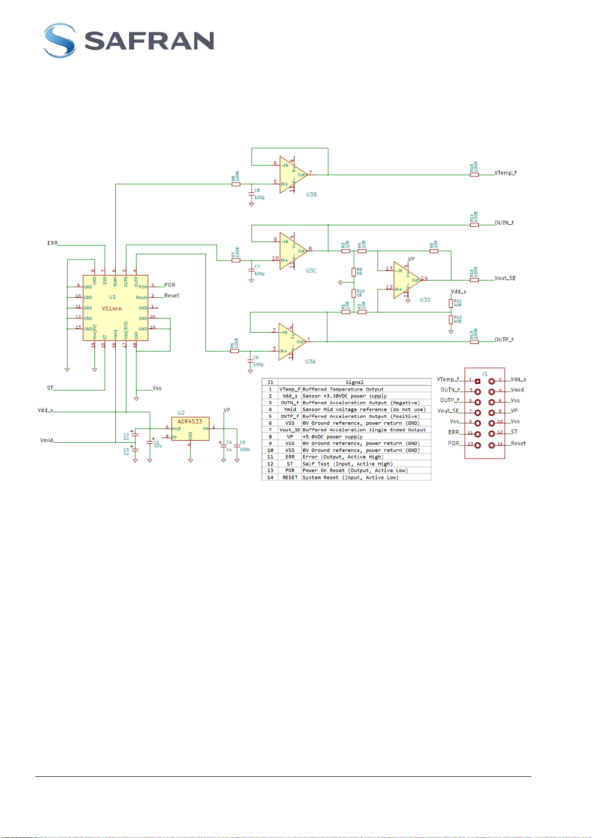
Component Value Function
U1 VS1000 Safran Colibrys Accelerometer
U2 ADR4533 3V3 Voltage Reference – Analog Devices ADR4533BRZ
U3 AD8574 Quad Operational Amplifier – Analog Devices AD8574ARZ
R1, R2, R3, R4 10 kΩ Voltage divider – 0402 resistor
R5 20 kΩ Voltage divider – 0402 resistor
R6, R7, R8 100 kΩ Low pass filter – 0402 resistor
R9, R10 5 kΩ Voltage divider – 0402 resistor
R11, R12 40 kΩ Voltage divider – 0603 resistor
R13, R14, R15, R16 100 Ω Output load – 0402 resistor
C1 10 µF Decoupling – 0603 capacitor
C2, C3, C4 1 µF Decoupling – 0402 capacitor
C5 100 nF Decoupling – 0402 capacitor
C6, C7, C8 100 pF Low pass filter – 0402 capacitor
J1 HEADER 7X2 Connector (if required*)
*The wires may also be soldered directly on the board.
Table 2: Bill of material
3 Operation
Handle with appropriate precautions and be done in accordance with strict ESD control.
It is the user choice to use the connector provided or to solder the signal wire lines
directly on the board. In both situation please follow the proper soldering process. Hand
soldering is recommended.
3.1 Power Up
Once the cabling done the EVBA can be powered up by applying the VP voltage level. The current consumption
and the reference voltage VDD shall be:
Parameter Designation [unit] Typical
Sensor +3.30V power supply VDD [VDC] 3.30
Board current consumption IP [mADC] 7.14

TECHNICAL NOTE
Safran Colibrys SA 30N.EVBA V2.10.16
Av. des Sciences 13 – 1400 Yverdon-les-Bains - Switzerland T +41 58 100 5000
www.safran-colibrys.com page 8 F +41 58 100 5001
3.2 Outputs
With the EVBA board placed horizontal in a quite environment will expose the sensor to an acceleration of 1g.
The corresponding level of the signals OUTP_f, OUTN_f and Vout_SE settles proportional to the range and
scale factor of the VS1000 mounted. The available ranges are ± 2g, 5g, 10g, 30g, 100g and 200g.
The typical readouts are at 1g acceleration:
Parameter Designation
[unit]
Typical
2g 5g 10g 30g 50g 100g 200g
OUTP OUTP [VDC] 2.325 1.920 1.785 1.695 1.677 1.663 1.657
OUTN OUTN [VDC] 0.975 1.380 1.515 1.605 1.623 1.636 1.643
Single-ended
output
VOUT_SE
[VDC] 2.325 1.920 1.785 1.695 1.677 1.663 1.657
With the EVBA operated in an ambient temperature of +25°C ± 3°C the Vtemp-f signal on J1/1 shall read:
Parameter Designation [unit] Typical
Vtemp buffered Vtemp_f [VDC] 1.210
The VS1000 accelerometer provides logic output signals:
Parameter Designation [unit] Typical
Error signal (flag) ERR [VDC] Vss
Power-on Reset signal (flag) POR [VDC] Vdd
3.3 Logic signals
Some functionalities can be controlled by applied logical signals according to the Table 3.
They all are referenced to the VS1000 Vdd (+3.3VDC) voltage level and proper
interfacing is required. A Logic HIGH level corresponds to the Vdd voltage level and a
logic LOW level to the Vss voltage level.
J1 / Pin#
Signal
Designation
12
ST
Self-test activation, active high
14
RESET
System reset signal, active low
Table 3
For the detailed function and effects of these signals please refer to the Datasheet of the VS1000 sensor.

TECHNICAL NOTE
Safran Colibrys SA 30N.EVBA V2.10.16
Av. des Sciences 13 – 1400 Yverdon-les-Bains - Switzerland T +41 58 100 5000
www.safran-colibrys.com page 9 F +41 58 100 5001
4 Ordering Information
The user will have to select the appropriate sensor range for his application (see VS1000 family data sheet) and
then order the corresponding EVBA version. Table 4 shows the range, Designation and Part number for each
available EVBAs.:
Range [g]
Designation
Part Number
±2
EVBA_2.0_VS1002.A
37628071
±5
EVBA_2.0_VS1005.A
37623081
±10
EVBA_2.0_VS1010.A
37625033
±30
EVBA_2.0_VS1030.A
37628084
±50
EVBA_2.0_VS1050.A
37629043
±100
EVBA_2.0_VS1100.A
37629061
±200
EVBA_2.0_VS1200.A
37629081
Table 4: EVBA ordering number
5 Disclaimer
EVBA_2.0_VS1000 evaluation kit is only intended for device evaluation, not for production purposes.
This manual suits for next models
1
Table of contents
Other Safran Motherboard manuals