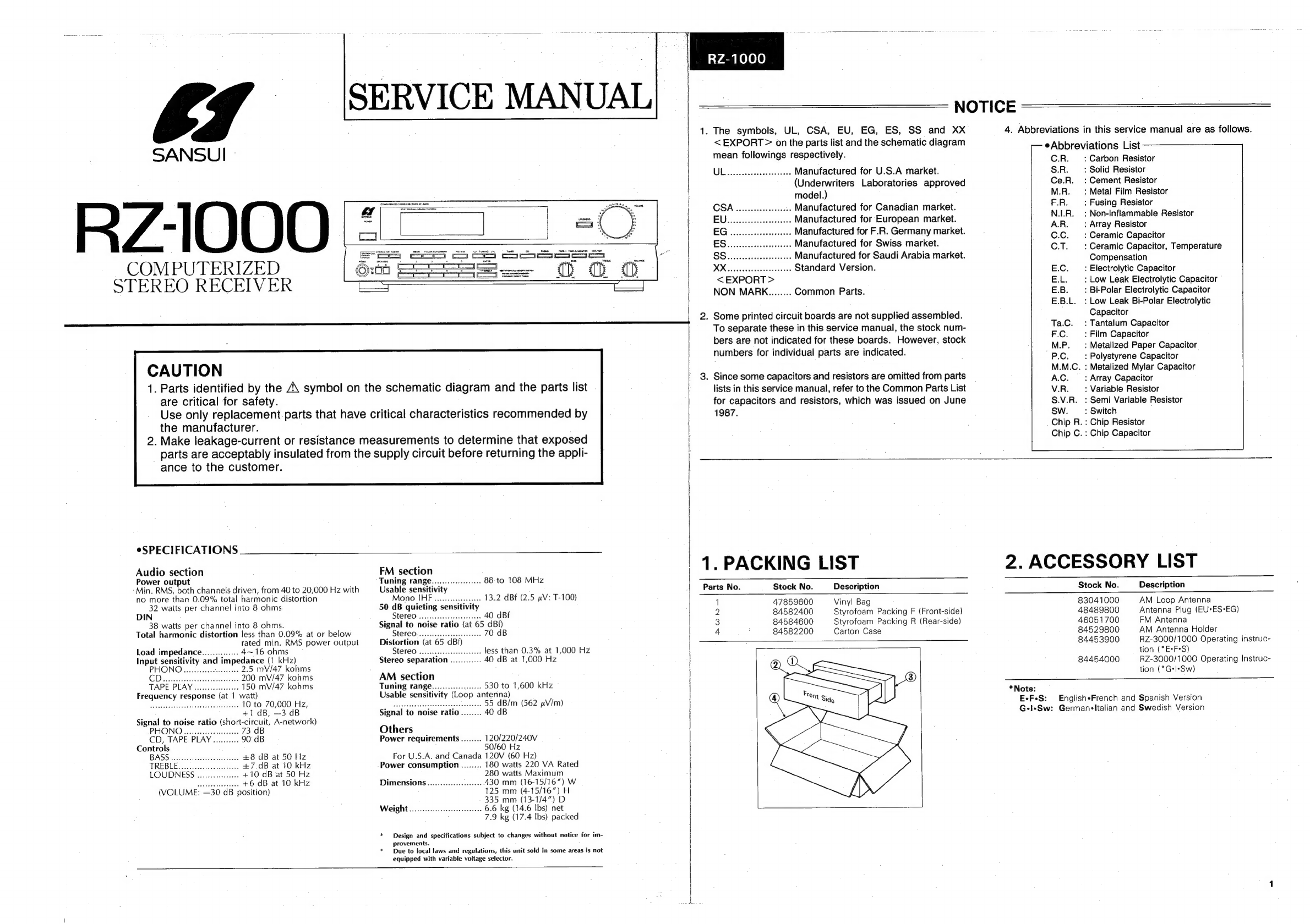
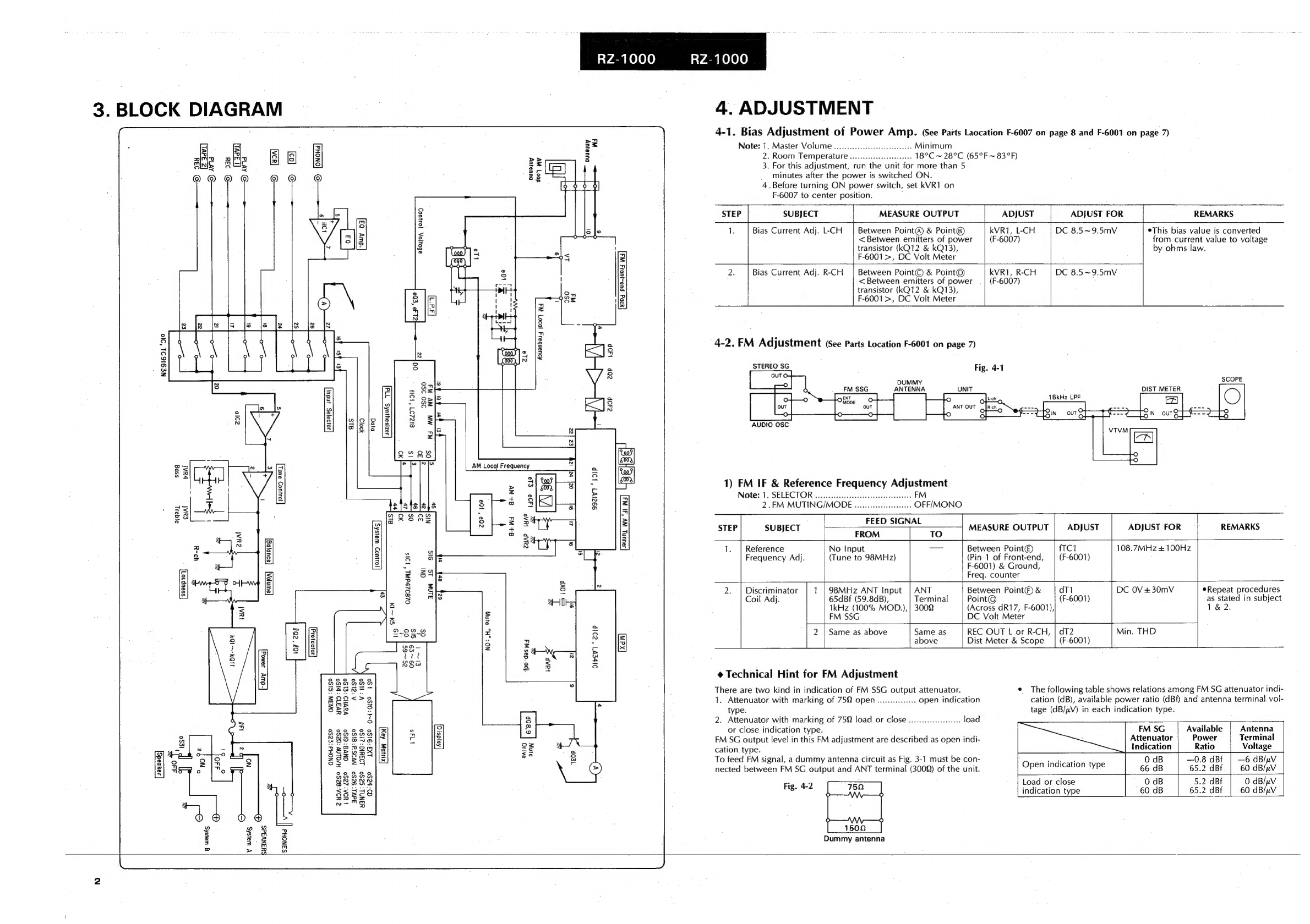
Sansui RZ-1500 User manual

ST
SANSUI
RZIS00O—
COMPUTERIZED
STEREO
RECEIVER
CAUTION
|
|
SERVICE
MANUAL!
NOTICE
For
servicing
RZ-1500,
please
refer
to
service
manual
for
the
RZ-1000
with
this
manual,
since
most
of
the
parts
and
circuits
employed
in
RZ-1500
are
in
common
with
the
RZ-1000.
On
the
parts
list,
the
changed
parts
are
specified
by
"®"
mark
on
top
of
the
Stock
No.
,
1.
Parts
identified
by
the
A
symbol
on
the
schematic
diagram
and
the
parts
list
are
critical
for
safety.
Use
only
replacement
parts
that
have
critical
characteristics
recommended
by
the
manufacturer.
2.
Make
leakage-current
or
resistance
measurements
to
determine
that
exposed
parts
are
acceptably
insulated
from
the
supply
circuit
before
returning
the
appliance
to
the
customer.
SPECIFICATIONS
Audio
section
Power
output
Min,
RMS,
both
channels
driven,
from
40
to
20,000
Fz
with
no
more
than
0.09%
total
harmonic
distortion
32
watts
per
channel
into
8
ohms
DIN
38
watts
per
channel
into
8
ohms.
Total
harmonic
distortion
less
than
0.09%
at
or
below
rated
min.
RMS
power
output
Load
impedance.............
4~16
ohms
Input
sensitivity
and
impedance
(1
kHz)
PHONO
i
csisccazssaseseseces
2.5
mV/47 kohms
Di
teen
clases
.
200
mV/47
kohms
TAPE PLAY
150.mV/47
kohms
Frequency
response
(at
|
watt)
seusvesbvonvsnqwencsnanesengonnees
10
to
70,000
Hz,
+1
dB,
—3
dB
Signal
to
noise
ratio
(short-circuit,
A-network)
PHONO
iscsapusnseatsrsedes
73
dB
CD,
TAPE
PLAY...
90
dB
Controls
BASS
vvevvonedneunssvesesvonens
+8
dB
at
50
Hz
TREBLE
cvsscsnsscngysenvnaves
+7
dB
at
10
kHz
LOUDNESS
cassssssvessuxcs
+10
dB
at
50
Hz
Sa
aaieaactntecete
+6
dB
at
10
kHz
(VOLUME:
—30
dB
position)
FM
section
Tuning
range...
cee
88
to
108
Mt
iz
Usable
sensitivity
Mono
JHE
oo...
13.2
dBf
(2.5
pV:
T-100)
50
dB
quicting
sensitivity
SECPES
cciccs
conrwaticessiiuense
40
dBf
Signal
to
noise
ratio
(at
65
dBA
SLORCO.
scxcqceceyeasapaxounsies
70
dB
Distortion
(at
65
d8Bf
SlereO
scseccanaassesadececisss
less
than
0.3%
at
1,000
Hz
Stereo
separation
............
40
dB
at
1,000
Fz
AM
section
Tuning
range...
530.to
1,600
kidz
Usable
sensitivity
(Loop
antenna)
.
Sidi
rak
caveasee
see
G
tn
tne
55
dB/m
(562
pV/m)
Signal
to
noise
ratio........
40
dB
Others
:
Power
requirements........
120/220/240V
50/60
Hz
For
U.S.A.
and
Canada
120V
(60
Hz)
Power
consumption
........
180
watts
220
VA
Rated
280
walts
Maximum
Dimensions
.................
430
mm
(16-15/16")
W
125
mm
(4-15/167)
FH
335
mm
(13-1/47)
D
Weight
ccsicccsessscscavcesreacsene
6.6
kg
(14.6
Ibs)
net
7.9
kg
(17.4
Ibs)
packed
*
Design
and
specifications
subject
to-changest
withoul
notice
far
ime
provements.
*
Due
to
local
laws
and
regulations,
this
unit
sald
in
seme
areas
is
not
equipped
with
variable
voltage
selector.

lIOTICE
Some
printed
circuit
boards
are
not
supplied
assembied.
To
separate
these
in
this
service
manual,
the
stock
numbers
are
not
indicated
for
these
boards.
However,
stock
numbers
for
individual
parts
are
indicated.
The
symbols,
EU
and
EG
on
the
parts
list
and
the
schematic
diagram
mean
followings
respectively.
BU
iessibeeetatee
Manufactured
for
European
market.
EG
iicstesccecetsee
Manufactured
for
F.R.Germany
market.
NON
MARK....
Common
Parts.
Sir.ce
some
capacitors
and
resistors
are
omitted
from
parts
lists
in
this
service
manual,
refer
to
the
Common
Parts
List
for
capacitors
and
resistors,
which
was
issued
on
June
1987.
|.
PACKING
LIST
arts
No.
Stock
No.
1
47859600
2
84582400:
3
84584600
4
®@
84648500
Description
Vinyl
Bag
Styrofoam
Packing
F
(Front-side)
Styrofoam
Packing
R
(Rear-side)
Carton
Case
4.
Abbreviations
in
this
parts
list
are
as
follows.
CLR.
:
Carbon
Resistor
S.R.
:
Solid
Resistor
Ce.R.
:
Cement
Resistor
MLR.
:
Metal
Film
Resistor
F.R.
:
Fusing
Resistor
NAIR.
:
Non-Inflammabie
Resistor
A.R.
__
:
Array
Resistor
C.C.
:
Ceramic
Capacitor
oa
:
Ceramic
Capacitor,
Temperature
Compensation
E.C.
—_:
Electrolytic
Capacitor
E.L.
:
Low
Leak
Electrolytic
Capacitor
E.B.
:
Bi-Polar
Electrolytic
”
Capacitor
Abbreviations
List
_____SSSsseeeseSsSSSSFSFSCSFSF
E.B.L.
:Low
Leak
Bi-Polar
Electrolytic
Capacitor
Ta.c.
:
Tantalum
Capacitor
FG.
:
Film
Capacitor
MP.
:
Metalized
Paper
Capacitor
P.C.
:
Polystyrene
Capacitor
M.M.C.
_:
Metalized
Mylar
Capacitor
A.C.
:
Array
Capacitor
V.R.
:
Variable
Resistor
$.V.R.
:
Semi
Variable
AResistor
SW.
>
Switch
Chip
R.
:
Chip
Resistor
Chip
C.
:
Chip
Capacitor
2.
ACCESSORY
LIST
Stock
No.
83041000
48489800
46051700
©
84606600
©
84458200
©
84458300
*Note:
Description
AM
Loop
Antenna
Antenna
Plug
FM
Antenna
AM
Antenna
Holder
Operating
Instruction
(*E*F*S)
Operating
Instruction
(*G+l*Sw)
E-F-S:
English*French
and
Spanish
Version
G-l-Sw:
Germansitalian
and
Swedish
Version
i~
eee
eG
onc
he

a
4.
PARTS
LIST
OF
BOARD
4-1.
F-6001
Main
Board
<Stock
No.01118305=EU
/
01118308=EG>
Parts
No,
Stock
No.
Description
Parts
No.
dZ1
49316600
FM
Frontend
Pack
eC24
Transistor
eTC1,2
dai
46834300
OTC144ES
dQ2
46393201
2SC2786
dQ3
46540801
2802878
eCF1
or
46604301
2803327
i
dQ4~7
46834300
DOTC144ES
el
dQs
46834200
OTA144ES
dag
46367101
2SC2603
eT1
er
48058801
28C1740S
eT2
dQ10,11
46834300
DTC144ES
eT3
1c
;
eVR1
diCi
48715100
LA1266
7
dlc2
48491000
LA3410A
4
«iC
dX01
83000200
Quartz
Element
.
fIC1
“Diode
{XO1
dD1~10
46464100
1$$133
“Diode
{TC1
dC4~8
48426900
22000pF
25V
C.C.
dc9
48103300
0.68uF
50V
E.B.
dC11
48662600
1O00pF
50V
C.C.
fL1
dC12,13
48102400
4.7nF
25V
E.B.
dC18
48663100
270pF
50V
C.C.
AC
dC27
@
48662600~-
100pF
50V
C.C.
iIC1
dC30
©
48426900
22000pF
25V
C.C.
iC2
dCF1,2
48064800
Ceramic
Filter
iC100
SFE10.7MS3GH
*Transistor
dli
83043200
Inductor
100H
:
kQ7
dLP1
©
83030101
Low
Pass
Filter
(EG)
A
kQt2
Ay
kQi3
dT1
83005900
FM
IF
Coil
dT2
83006000
FM
IF
Coil
kC34
dT3
e
48791700
CH
Filter
(EG)
Ay
kR34,35
A
dR9
46227800
|
10Q
1/2W
N.I.R.
A
DRi9
46228200
22Q
1/2W
N.IR.
kL2,3
dVR1
83007600
200kQ
S.V.R.,
“Transistor
FM
Stereo
Sep.
Adj.
at
dVR2
83007600
200kQ
S.V.R.,
Muting
Level
Adj.
lQ2
*Transistor
»
*Diode
eQi,2
46367001
2SA1115
D1
‘
or
48058601
2SA933S
eQ3
46367101
2S8C2603
*Zener
Diode
or
48058801
2S8C01740S
IDZ2
“FET
A
IFA
aFT2
46643501
2SK163-K2
or
46643502
2SK163-L1
-
*Transistor
or
46643601
2SK117-Y
A
mai
or
46643602
2SK117-GR
A
mQ2
-
mQ3
*Diode
eDi
46146300
KV1236Z2
A
mQ4,5
(Variable
Capacitance)
eD2,3
46464100
1$S$133
“Diode
mD1~4
eC10~12
48426900
22000pF
25V
C.C.
mD5
eCcié6
48426900
22000pF
25V
C.C.
eCi7
48666200
O0.01pF
50V
C.C.
«Zener
Diode
eC20,21
48426900
22000pF
25V
C.C.
mDZ1
eC23
48663800
1000pF
50V
C.C.
mO0Z2
or
or
or
or
or
Stock
No.
48103500
46095700
46162900
48865700
83020300
48528900
83005700
83013400
83007500
49317500
83004400
|
46095700
46162900
83042600
46078900
48663000
48662600
03067401
48577901
48577801
48426900
46542200
83020100
48863701
48863901
46367001
48058601
46464100
48551900
83049000
48581701
03083901
46367101
48058801
48064001
83049400
83002100
48552900
48555300
A
Description
2.2uF
50V
E.B.
30pF
Trimmer
Capacitor
3O0pF
Trimmer
Capacitor
BFCFL-450
Ceramic
Filter
39pH
Coil
AM
ANT
Coil
AM
OSC
Coil
AM
IF
Coil
100kQ
S.V.R.,
AM
Auto
Stop
Level
Adj.
LC7218
Quartz
Element
30pF
Trimmer
Capacitor
S3OpF
Trimmer
Capacitor
10H
Inductor
MS218L
220pF
SOV
C.C.
1O0pF
50V
C.C.
2801845
2SC3853
2SA1489
22000pF
25V
0.2Q
2W
Ce.R.
0.82nH
Inductor
2302857
2801473
2SA1115
2SA933S
18S133
MTZ4.7CT-77
Fuse
4A
280438
2S0313HP
2SC2603
28C01740S
2SA1284
1N4003
KBU4D
MTZ6.8AT-77
MTZ13CT-77

RZ-1500
<F4001>
Parts
No
Stock
No.
Description
mDZ3
48555100
MTZ13AT-77
mDZ4
48552100
MTZ5.1BT-77
or
48552200
MTZ5.1CT-77
mDZ5
48558000
MTZ30BT-77
or
48558100
MTZ30CT-77
A
mRt
46249700
2202
1/2W
N.1.R.
A
mR4
46623700
33Q
2W
N.IR.
Ay
mR100
46227400
4.7
1/2W
N.IR.
Av
mA101
46227800
10Q
1/2W
NLR.
mC8,9
e
49350500
mC10,11
©
08680400
Transistor
°0Q1
46540801
or
46604301
0Q2
46367101
or
48058801
0Q3
46834200
0Q21
48229400
4c
olCi
-
49312200
olC2
46147700
*Diode
0DZ21
®
48554300
0C1
48660200
®
48662600
oC2
48659400
@
48663000
0C3
48660200
®
48662600
oC4
48659400
©
48662600
oC5
48663000
@
48662600
Ay
pFt
83024000
49320400
48528400
48528300
48528200
48987400
46947500
5600uF
SOV
E.C.
0.01pF
S00V
C.C.
2SC2878
2803327
2SC2603
28C01740S
DTA144ES
DTA114TS
TC9163N
MS5218L
MTZ10C
47pF
50V
C.C.
(EU)
100pF
SOV
C.C.
(EG)
22pF-50V
C.C.
(EU)
220pF
50V
C.C.
(EG)
47pF
50V
C.C.
(EU)
100pF
S0V
C.C.
(EG)
229F
50V
C.C.
(EU)
100pF
50V
C.C.
(EG)
220pF
50V
C.C.
(EU)
100pF
SOV
C.C.
(EG)
Fuse
3.15A
2P
Antenna
Terminal
2P
Pin
Jack
Terminal,
PHONO
6P
Pin
Jack
Terminai,
TAPE
1/CD
4P
Pin
Jack
Terminal,
TAPE2
2P
Pin
Jack
Terminal,
VCR/IVDP
8P
Speaker
Terminal
4-2,
F-6002
SPEAKER
IMPEDANCE
Switch
Board
Parts
No.
Stock
No.
0S32
49338500
Ay
pF3
83023500
AN
pS2
*®
07204700
Description
Side
SW.,
SPEAKER
IMPEDANCE
Fuse
3A
(ES)
Voltage.
Selector
4-3,
F-6003
Tuner
Control
and
Operating
Switch
Board
<stock
No.0111860s>
Parts
No.
Stock
No.
Description
«Diode
oD1~11
46464100
18S133
oS1
©
83049900
Push
SW.,
1
(Preset)
<F-6003>
Parts
No.
Stock
No.
Description
oS2
©
83049900
Push
SW.,
2
(Preset)
0S3
®
83049900
Push
SW.,
3
(Preset)
oS4
©
83049900
Push
SW.,
4
(Preset)
oSs
®
83049900
Push
SW.,
5
(Preset)
oSé
©
83049900
Push
SW.,
6
(Preset)
oS7
©
83049900
Push
SW.,
7
(Presat)
oS8
©
83049900
Push
SW.,
8
(Preset)
oS9
@
83049900
Push
SW.,
9
(Preset)
oSi0
®
83049900
Push
SW.,
0
(Preset)
0$11
®
83049900
Push
SW.,
~
(TUNING)
0S1i2
®
83049900
Push
SW.,
v
(TUNING)
0S13
*
83049900
Push
SW.,
CHARACTER
0S14
e
83049900
Push
SW.,
CLEAR
0S15
©
83049900
Push
SW.,
MONO
0Si6
®
83049900
Push
SW.,
ENTER
o0S17
®
83049900
Push
SW.,
F
DIRECT
0Si8
®
83049900
Push
SW.,
P
SCAN
oS19
©
83049900
Push
SW.,
BAND
0S20
*®
83049900
Push
SW.,
AUTO
0S23
©
83049900
Push
SW.,
PHONO
oS24
*®
83049900
Push
SW.,
CD
oS25
*®
83049900
Push
SW.,
TUNER
oS26
©
83049900
Push
SW.,
TAPE-1
0S27
®
83049900
Push
SW.,
TAPE-2
0S28
*
83049900
Push
SW.,
VCR/VDP
Transistor
sQi~3
e
46367101
2SC2603
sQ4~6
46719900
DTC124ES
sQ7
46367101
2862603
or
48058801
28C01740S
sQQ
46834300
DTC144ES
4c
slC1
@
49346400
TMP47C870N-4612
sxO1
48241600
Ceramic
OSC
Element
*
*Diode
sD1~5
46464100
1$$133
sFL1
49317100
FL.
Display
Tube
CP3023
'
§R10,11
©
49346300
10kQ
x
ZAR.
sC4
©
48388400
4700uF
6.3V
E.C.
4-4,
F-6004
Speakers
Switch
Board
Parts
No.
Stock
No.
Description
kL
83020100
inductor
A,
kR39,40
46227800
10Q
1/2W
NILA.
Ay
kR41
46229400
2202
1W
NILA.
0S31
83045900
Push
SW.,
SPEAKERS
46879600
Jack,
PHONES
4-5.
F-6006
Master
and
Tone
Control
Volume
Board
Parts
No.
Stock
No.
Description
iC
jici
46673800
M5218P
jc4
48660200
47pF
50V
C.C.
jc9
48663400
470pF
50V
C.C.
jC17
*
48663000
220pF
SOV
C.C.
to
be
continued
3

lel
>
DB
is
<F-6006>
Parts
No.
Stock
No.
Description
Ay
jR21
46229000
100Q
1/2W
NLR.
jVR1
©
83046600
150kQ
(B)
x
2
V.R.,
Masteer
jvR2
83013000
250kQ
V.R.,
BALANCE
jVR3
83012800
.
50kQ
(C)
V.R.,
TREBLE
jVR4
83012800
50kQ
(C)
V.R.,
BASS
jS1
83046700
Push
SW.,
LOUDNESS
4-6.
F-6007
Power
Amp.
Board
<Stock
No.
01119005>
Parts
No.
Stock
No.
Description
¢Transistor
kQ1
46367001
2SA1115
or
46392001
2SA1175
kQ2
48577701
2SA1349
kQ3,4
46728301
2SC2705
or
48113001
2802229
kQ5
03064001
2801904
or
46128101
28C2911
kQ6
03007901
2SA899
or
46128001
2SA1209
kQ8
48061801
2803244
kag
48064001
2SA
1284
kQ10
48061801
2803244
kQ11
48064001
2SA1284
A
kRI1
46230200
1kQ
1/2W
NLR.
Ay
kRi2
46229200
150Q
1/2W
N.LR.
A
kRI6
46230200
5.6kQ
1/2W
NLR.
Ay
kR19
46228500
39Q
1/2W
NLR.
Ay
kR20
46229200
150Q.
1/2W
N.1.R.
Ay
kR21
46230200
1kQ
1/2W
NLR.
AN
kR23,24
46228400
33Q
1/2W
NLR.
A
kR29
46230200
1kQ
1/2W
N.LR.
Av
kR30
46229100
120Q
1/2W
N.LR.
Ay
kR32,33
46227400
4.7Q
1/2W
NLR.
*Diod
kD1
46464100
1$S$133
kVR1
48078600
1kQ
S.V.R.,
Bias
Current
Adj.
‘RZ-1500°
5.
OTHER
PARTS
Parts
List
<Front
View>
Parts
No.
QNAMOR
WP
+
©
0
1
12
13
14
15
16
AN
Stock
No.
®
84601200
49317100
©
84578510
84580300
83046700
84586900
®
83046600
84580100
83013000
83012800
©
83049900
84580000
83045900
©
84586400
46579600
84579700
83049200
Parts
List
<Top
View>
Parts
No.
Al
2
A
3
>
PBB
on
ane
Stock
No.
83046505
83002500
07204700
83000600
48913500
49543000
46947500
48987400
48528200
48528300
AQEDD
ANA
SOU
COM
84528300
49320400
Description
Front
Panei
Ass’y
CP-3023
FL.
Display
Tube
Bonnet
Push
Knob,
LOUDNESS
Push
SW.,LOUDNESS
Knob,
MASTER
150kQ
(B)
x
2V.R.,
MASTER
Knob,
BALANCE-
TREBLE-BASS
250kQ
V.R.,
BALANCE
50kQ
(C)
x
2
V.R.,
TREBLE-BASS
Push
SW.,
Operation
Push
Knob,
SPEAKERS
Push
SW.,
SPEAKERS.
Leg
Jack,
PHONES
Knob,
POWER
Push
SW.,
POWER
Description
Power
Transformer
AC
Outlet
:
Slide
SW.,
Voltage
Selector
Power
Supply
Cord
Strain Relief
Slide
SW.,
SPEAKER
IMPEDANCE
SELECTOR
8P
Speaker
Terminal
2P
Pin
Jack
Terminal,
VCR/VDP
4P
Pin
Jack
Terminal,
TAPE-2
6P
Pin
Jack
Terminal,
TAPE-1°CD
2P
Pin
Jack
Terminai,
PHONO
Ground
Terminal
2P
Antenna
Terminal

«Front
View
“Top
View
@
@
@\|
©
©
@
OGD
WO
:
oe
omorn
yeh
ana.
ol
a
Sees
ae
oases
ee
ae
a
A.
F-6002
C
SANSU!
ELECTRIC
CO.,
LTD.:
New
River
Building.
10-14,
Shinkawa
1t-chome,
Chuo-ku
Tokyo
104,
Japan
PHONE:
(03)5566-1024
FAX:
(03)5566-1027
(International
Division)
1250
Valtey
Brook
Ave.
Lyndhurst,
N.J.
07071
U.S.A.
17150
South
Margay
Ave.
Carson.
California
90746
U.S.A.
SANSUI
DEUTSCHLAND
GMBH:
Paui
Ehriich
Strasse
8,
6074
Rodermark
2,
West
Germany
SANSUI
WKS
ARNE
Ht
ABH
1-10-14
(F104)
(SM2-205)
Printed
in
Japan
(1990.10.P)
—
<Stock
No.36554600>
SANSUI
USA
INC.:

SANSUI
>
RZ1IOO
COMPUTERIZED
STEREO
RECEIVER
CAUTION
1.
Parts
identified
by
the
Z\
symbol
on
the
schematic
diagram
and
the
parts
list
are
critical
for
safety.
Use
only
replacement
parts
that
have
critical
characteristics
recommended
by
the
manufacturer.
2.
Make
leakage-current
or
resistance
measurements
to
determine
that
exposed
parts
are
acceptably
insulated
from
the
supply
circuit
before
returning
the
appli-
ance
to
the
customer.
SPECIFICATIONS
Audio
section
Power
output
Min.
RMS,
both
channels
driven,
from
40
to
20,000
Hz
with
no
more
than
0.09%
total
harmonic
distortion
32
watts
per
channel
into
8
ohms
DIN
38
watts
per
channel
into
8
ohms.
Total
harmonic
distortion
less
than
0.09%
at
or
below
rated
min.
RMS
power
output
Load
impedance..............
4~16
ohms
Input
sensitivity
and
impedance
(1
kHz)
PHONG
wiescin
gon
ets
eieetad
2.5
mV/47
kohms
CDi
reals.
be
200
mV/47 kohms
TAPE
PLAY
150
mV/47 kohms
Frequency
response
(at
1
watt)
stguoteeadtetossctananegeuceesaee
10
to.
70,000
Hz,
+1
dB,
—3
dB
Signal
to
noise
ratio
(short-circuit,
A-network)
PHONO...
edie
teeeeee
ee
73
dB
CD,
TAPE
PLAY..........
90:
dB
Controls
BASS
+8
dB
at
50
Hz
TREBLE
+7.dB
at
10
kHz
+10
dB
at
50
Hz
+6
dB
at
10
kHz
(VOLUME:
—30
GB
position)
FM
section
Tuning
range................0
88
to
108
MHz
Usable
sensitivity
Mono
IHF
...ccsceseeeeeees
13.2
dBf
(2.5
pV:
T-100)
50
dB
quieting
sensitivity
=
10
40
dBf
Signal
to
noise
ratio
(at
65
dBf)
StOreO
i
seectieweiaaesiee
eee
70
dB
Distortion
(at
65
dBf)
StEreO
.o.eeeeeeeeeeeeeeeeeees
less
than
0.3%
at
1,000
Hz
Stereo
separation
............
40
dB
at.1,000
Hz
AM
section
Tuning
range...............0...
530
to
1,600
kHz
Usable
sensitivity
(Loop
antenna)
oth
ha
seth
ean
55
dB/m
(562
zV/m)
Signal
to
noise
ratio
........
40
dB
Others
Power
requirements
........
120/220/240V
50/60
Hz
For
U.S.A.
and
Canada
120V
(60
Hz)
Power
consumption
........
180
watts
220
VA
Rated
280
watts
Maximum
Dimensions
......................
430
mm
(16-15/16”)
W
125
mm
(4-15/16”)
H
335
mm
(13-1/4”)
D
Weight
...............:
eee
6.6
kg
(14.6
Ibs)
net
7.9
kg
-(17.4
lbs)
packed
*
Design
and
specifications
subject
to
changes
without
notice
for
im-
provements.
:
*
Due
to
local
Jaws
and
regulations,
this
unit
sold
in
some
areas
is
not
equipped
with
variable
voltage
selector.
;
ce
ea
a
RZ-1000
1.
The
symbols,
UL,
CSA,
EU,
EG,
ES,
SS
and
XX
<EXPORT>
on
the
parts
list
and
the
schematic
diagram
mean
followings
respectively.
Ube
csvosteesdeerenss
Manufactured
for
U.S.A
market.
(Underwriters
Laboratories
approved
model.)
CSA
secede:
Manufactured
for
Canadian
market.
Bs
cseaveeteeestees
Manufactured
for
European
market.
EG
aise
ae
Manufactured
for
F.R.
Germany
market.
ES
wi
clish
tai
deeds.
Manufactured
for
Swiss
market.
GS
vc
cictisscets
Restore
Manufactured
for
Saudi
Arabia
market.
MK
se
akedus
Qeeiiamees
Standard
Version.
<EXPORT>
NON
MARK........
Common
Parts.
.
Some
printed
circuit
boards
are
not
supplied
assembled.
To
separate
these
in
this
service
manual,
the
stock
num-
bers
are
not
indicated
for
these
boards.
However,
stock
numbers
for
individual
parts
are
indicated.
.
Since
some
capacitors
and
resistors
are
omitted
from
parts
lists
in
this
service
manual,
refer
to
the
Common
Parts
List
for
capacitors
and
resistors,
which
was
issued
on
June
1987.
1.
PACKING
LIST
Parts
No.
Stock
No.
Description
1
47859600
Vinyl
Bag
2
84582400
Styrofoam
Packing
F
(Front-side)
3
84584600
Styrofoam
Packing
R
(Rear-side)
4
84582200
Carton
Case
NOTICE
4.
Abbreviations
in
this
service
manual
are
as
follows.
Capacitor
SW.
:
Switch
eAbbreviations
List
C.R.
—:
Carbon
Resistor
S.R.
—:
Solid
Resistor
Ce.R.
:
Cement
Resistor
M.R.
:
Metal
Film
Resistor
F.R.
—
:
Fusing
Resistor
N.I.R.
:
Non-Inflammable
Resistor
A.R.
:
Array
Resistor
C.C.
_:
Ceramic
Capacitor
C.T.
|:
Ceramic
Capacitor,
Temperature
Compensation
E.C.
_
:
Electrolytic
Capacitor
E.L.
:
Low
Leak
Electrolytic
Capacitor
°
E.B.
_
:
Bi-Polar
Electrolytic
Capacitor
E.B.L.
:
Low
Leak
Bi-Polar
Electrolytic
Ta.C.
:
Tantalum
Capacitor
F.C.
:
Film
Capacitor
_M.P,
—
:
Metalized
Paper
Capacitor
P.C.
—_:
Polystyrene
Capacitor
M.M.C.
:
Metalized
Mylar
Capacitor
A.C.
—
:
Array
Capacitor
V.R.
:
Variable
Resistor
S.V.R.
:
Semi
Variable
Resistor
Chip
R.
:
Chip
Resistor
Chip
C.
:
Chip
Capacitor
2.
ACCESSORY
LIST
Stock
No.
Description
83041000
AM
Loop
Antenna
48489800
Antenna
Plug
(EU*ES-EG)
46051700
FM
Antenna
84529800
AM
Antenna
Holder
84453900
RZ-3000/1000
Operating
Instruc-
tion
(*E+F+S)
84454000
RZ-3000/1000
Operating
Instruc-
tion
(*G-+l*-Sw)
*Note:
E*FeS:
EnglisheFrench
and
Spanish
Version
Gel-Sw:
Germaneltalian
and
Swedish
Version

RZ-1000
RZ-1000
3.
BLOCK
DIAGRAM
|
4.
ADJUSTMENT
4-1.
Bias
Adjustment
of
Power
Amp.
(ee
Parts
Laocation
F-6007
on
page 8
and
F-6001
on
page
7)
Note:
1.
Master
Volume
..........cceseeeeeeeeeneeeees
Minimum
2.
Room
Temperature
.
...
18°C
~
28°C
(65°F
~
83°F)
3.
For
this
adjustment,
run
the
unit
for
more
than
5
minutes
after
the
power
is
switched
ON.
4.
Before
turning
ON
power
switch,
set
kVR1
on
F-6007
to
center
position.
g
STEP
SUBJECT
MEASURE
OUTPUT
ADJUST ADJUST
FOR
REMARKS
=
1:
Bias
Current
Adj.
L-CH
|
Between
Point@®
&
Point®)
kVR1,
L-CH
DC
8.5~9.5mV
eThis
bias
value
is
converted
s
<
Between
emitters
of
power
|
(F-6007)
from
current
value
to
voltage
s
transistor
(kKQ12
&
kQ13),
by
ohms
law.
Zz
F-6001>,
DC
Volt
Meter
:
3
2:
Bias
Current
Adj.
RCH
|
Between
Point©
&
Point®
kVR1,
R-CH
DC
8.5~9.5mV
a
<
Between
emitters
of
power
(F-6007)
:
a
transistor
(kQ12
&
kQ13),
a
F-6001
>,
DC
Volt
Meter
4-2.
FM
Adjustment
(See
Parts
Location
F-6001
on
page
7)
Aouanbai4
(D207
W4
STEREO
SG
Fig.
4-1
NE9IGI1
‘910
DUMMY
FM
SSG
ANTENNA
2S0
ISO
Ws
MW
WV
W4
AUDIO
OSC
10}9ajag
jndu|
sazisayyuhS
Wd
BIZLIT
‘SONS
3
g
1)
FM
IF
&
Reference
Frequency
Adjustment
el
=
Note:
1.
SELECTOR
.0......:cseseesseereeceeeeeeeeeeeens
FM
S
=
2.FM
MUTING/MODE
......seessseeeeeeee
OFF/MONO
=
jt
8
E
FEED
SIGNAL
g
8
=
STEP
SUBJECT
MEASURE
OUTPUT
|
ADJUST
ADJUST
FOR
REMARKS
s
s
FROM
TO
3
aq
[ea
Ee
ina
OS
ee
a
ee
Pe
al.
=
Sep
eas
ire
ica
amar
teem
|
¢
&
o
=
1.
|
Reference
No
Input
aaa
Between
Point®©
fTC1
108.7MHz
+
100Hz
2
5 ®
Frequency
Adj.
(Tune
to
98MHz)
(Pin
1
of
Front-end,
|
(F-6001)
=
=
su
F-6001)
&
Ground,
=
SA
Freq.
counter
e~
3
é
2.
|
Discriminator
1
|
988MHz
ANT
Input
|
ANT
Between
Point)
&
dT1
DC
OV
+
30mV
*Repeat
procedures
a
”
Coil
Adj.
65dBf
(59.8dB),
Terminal
Point©
(F-6001)
as
stated
in
subject
TkHz
(100%
MOD.),|
3000
(Across
dR17,
F-6001),
;
1&2.
FM
SSG
DC
Volt
Meter
5
2
|
Same
as
above
Same
as
REC
OUT
L
or
R-CH,
|
dT2
Min.
THD
2
=
above
Dist
Meter
&
Scope
|
(F-6001)
3
5
——
2
ES
a
°o
7
¢
Technical
Hint
for
FM
Adjustment
n
au
There
are
two
kind
in
indication
of
FM
SSG
output
attenuator.
¢
The
following
table
shows
relations
among
FM
SG
attenuator
indi-
ee
1.
Attenuator
with
marking
of
750
open..............
open
indication
cation
(dB),
available
power
ratio
(dBf)
and
antenna
terminal.
vol-
52
type.
tage
(dB/pV)
in
each
indication
type.
3
2.
Attenuator
with
marking
of
750
load
or
close
.........
eee
load
BBD
i
or
close
indication
type.
FM
SG
Available
Antenna
B8o
FM
SG
output
level
in
this
FM
adjustment
are
described
as
open
indi-
Attenuator
Power
Terminal
Ree
Se
cation
type.
Indication
Ratio
Voltage
Soxnz2z
ae
P P : ‘
296
To
feed
FM
signal,
a
dummy
antenna
circuit
as Fig.
3-1
must
be
con-
Open
indication
type
aoe
cH
=
Soy
nected
between
FM
SG
output
and
ANT
terminal
(300)
of
the
unit.
Load
or
close
5.2
dBf
0
dB/uV
indication
type
65.2
dBf
60
dB/nV
AdVL:
9259
NVISd:
gISo
Y3NNL:
S2So
LO3yId:
21S°
2
YIA:82S9
H/OLMW
:0eS°
a9:
2go
bYOA:
Lease
Dummy
antenna
Sua4v3dS

RZ-1000
5.
PARTS
LIST
OF
BOARD
5-1.
F-6001
Main
Board
<Stock
No.
01118301
=
XX-SS/01118302
=
UL-CSA/01118305
=
EU-ES/01118308
=
EG
>
Parts
No.
Stock
No.
Description
dZ1
49316500
FM
Frontend
Pack
(XX*UL*CSA:SS)
49316600
FM
Frontend
Pack
(EU:ES-EG)
Transistor
dot
46834300
DTC144ES
da2
46393201
2SC2786
dQ3
46540801
2SC2878
;
or
46604301
2SC3327
dQ4~7
46834300
DTC144ES
dQ8
46834200
DTA144ES
dag
46367101
2SC2603
or
48058801
2SC1740S
dQ10,
11
46834300
DTC144ES
elC
dic
48715100
LA1266
diC2
48491000
LA3410A
dx0O1
83000200
Quartz
Element
Diode
dD1~9
46464100
1$S$133
dc4~8
48426900
22000pF
25V
C.C.
dcg
48103300
0.68nF
50V
E.B.
dC11
48662600
~
100pE
5OV
C.C.
dC12,
13
48102400
4.74F
25V
E.B.
dC18
48663100
270pF
50V
C.C.
dC27
48426900
22000pF
25V
C.C.
dCF1,
2
83000000
Ceramic
Filter
SFE10.7MS2
;
(XX-SS*UL*CSA)
48064800
Ceramic
Filter
SFE10.7MS3GH
(EU-ES-EG)
dL1
83043200
Inductor
100nH
dT1
83005900
FM
IF
Coil
dT2
83006000
FM
IF
Coil
dT3
46202400
CH
Filter
(EG)
A\dR9
46227800
10Q
1/2W
N.1R.
A\dR19
46228200
220
1/2W
NAAR.
dVR1
83007600
200k9
S.V.R.,
FM
Stereo
Sep.
Adj.
dVR2
83007600
200kQ
S.V.R.,
FM
Muting
Level
Adj.
¢Transistor
eQ1,
2
46367001
2SA1115
or
48058601
2SA933S
eQ3
46367101
2SC2603
or
48058801
2SC1740S
eFET
eFT2
46643501
2SK163-K2
or
46643502
2SK163-L1
or
46643601
2SK117-Y
or
46643602
2SK117-GR
Diode
eD1
46146300
KV1236Z2
(Variable
Capacitance)
eD2,
3
46464100
188133
Parts
No.
eC10~12
eCi6
eCi7
eC20,
21
eC23
eC24
eTC1,
2
eCF1
eL1
eT1
eT2
eT3
eVR1
eIC
fIC1
fXO1
fTC1
fL1
elC
iIC1
iC2
¢Transistor
kQ7
A\kQ12
AkQ13
A\kR34,
35
Transistor
101
1Q2
Zener
Diode
IDZ2
AIF1
¢Transistor
Ama
AmQ2
mQ3
AvmQ4
AvmO5
Diode
AmD1
AmD2
AmD3
AvmD4
AvmD5
fe)
fe)
Ol
0
fe)
r
foal
r
r
=
Stock
No.
48426900
48426900
48666200
48426900
48663800
48103500
46095700
46162900
48865700
83020300
48528900
83005700
83013400
83007500
49317500
83004400
46095700
46162900
83042600
46078900
48663000
03067401
48677901
48577801
46542200
48863701
48863901
46367001
48058601
48551900
83049000
48581701
03083901
46367101
48058801
48064001
48064001
83024700
83024700
83024700
83024700
83002100
Description
22000pF
25V
22000pF
25V
C.
Vv
0.01pF
50V
22000pF
25
1OO0pF
50V
C.C.
2.2uF
50V
E.B.
C.C.
C.C.
C,
Ge,
30pF
Trimmer
Capacitor
30
pF
Trimmer
Capacitor
BFCFL-450
Ceramic
Filter
39pH
Coil
AM
ANT
Coil
AM
OSC
Coil
AM
IF
Coil
100k
S.V.R.,
AM
Auto
Stop
Level
Adj.
LC7218
Quartz
Element
30pF
Trimmer
Capacitor
30pF
Trimmer
Capacitor
10H
Inductor
M6218L
220pF
50V
C.C.
2801845
2SC3853
2SA1489
0.20
2W
Ce.R
2SC2857
25C1473
2SA1115
2SA933S
MTZ4.7CT-77
Fuse
4A
28D438
2SD313HP
2SC2603
28C1740S
25A1284
2SA1284
1N4003
1N4003
:
i
1N4003
;
1N4003
KBU4D

RZ-1000
2)
FM
STEREO
Adjustment
Note:
1.
SELECTOR
...........cceccssseeeeeceeeeeeeeeees
FM
FEED
SIGNAL
FROM
TO
98MHz
ANT
Input
65dBf
|
ANT
(59.8dB),
FM
SSG,
Pilot
Terminal
19kHz
(9%
MOD.),
R
or
L}
3000
MODE
1kHz+
Pilot
(100%
MOD.),
STEREO
SG.
2.
|
Muting
Level]
98MHz
ANT
Input
20dBf
|
Same
as
Adj.
(14.8dB),
FM
SSG,
Pilot
above
19kHz
(9%
MOD.),
Lor
R
MODE
1kHz+
Pilot
(100%
MOD.),
STEREO
SG.
-
FM
MUTING/MODE
...........
eee
AUTO
No
STEP|
SUBJECT
MEASURE
OUTPUT
ADJUST
ADJUST
FOR
REMARKS
1.
|
Separation
Confirm
R>LCH
Adj.
REC
OUT
L-CH,
VTIVM
&
SCOPE
(F-6001)
REC
OUT
R-CH,
VTVM
&
SCOPE
Max.
Separation
Stereo
indicator
or
dVR2
Stereo
indicator
turns
OUTPUT
(L-CH
or
(F-6001)
On
or
Output
Signal
R-CH),
VTVM
&
|
comes
out
SCOPE
Sea
(eee
Na
Oe
ee
4-3.
AM
Adjustment
(See
Parts
Location
F-6001
on
page
7)
1)
AM
IF
Adjustment
&
Tuning
Adjustment
Note:
1.
SELECTOR
..........cccccccsssssseeeeeceeceeses
AM
2.
Connect
Fig.
4-3
AM
SSG
FEED
SIGNAL
FROM
1400kHz
(9kHz
step)
ANT
or
1404kHz
(10kHz
Terminal
step)
ANT
Input
55dB
400Hz
(30%
MOD.),
AM
SSG
2.
|
531kHz
(9kHz
step)}
No
Input
or
530kHz
(10kHz
step)
Tuning
Adj.
3.
|
1602kHz
(9kHz
No
Input
4
STEP
SUBJECT
MEASURE
OUTPUT
ADJUST
ADJUST
FOR
REMARKS
IF
Coil
Adj.
REC
OUT
L
or
R-CH,
Max,
Waveform
VTVM
&
SCOPE
Between
Point@®
(col-
|
eT2
DC
1V
*Repeat
procedures
lector
of
eQ3)
&
GND,
(F-6001)
as
stated
in
subject
2
DC
Volt
Meter
&
3.
Same
as
above
eTC2
DC
8V
(9kHz
step)
step)
or
1710kHz
(F-6001)
DC
10V
(10kHz
step)
(10kHz
step)
Tuning
Adj.
4.
|
603kHz
(9kHz
step)|
603kHz
(or
600kHz)
ANT
REC
OUT
eT1
Max.
Output
or
600kHz
(10kHz
|
ANT
Input
OdB
400Hz
|
Terminal]
L-CH
or
R-CH,
(F-6001)
step)
RF
Adj.
(30%
MOD.),
AM
SSG
VTVM
&
Scope
5.
|
1404kHz
(9kHz
1400kHz
(or
1400kHz)
|
Same
as
|
Same
as
above
eTCi
Max.
Output
step)
or
1400kHz
|
ANT
Input
30dB
400Hz]
above
(F-6001)
(10kHz
step)
(30%
MOD.),
AM
SSG
RE
Adj.
6.
|
Auto
Stop
Level
999kHz
(9kHz
step)
or
|
Same
as
|
Point®
(Pin
8
of
diC1),}
eVR1
Low
Level
(OV)
»
|
Adj.
1000kHz
(10kHz
step)
|
above
DC
Volt
Meter
(F-6001)
ANT
Input
65dB
400Hz
(30%
MOD.),
AM
SSG
wo)
ns
|
*
Notice
when
the
frequency-step
of
AM
broardcasting
is
set
to
9kHz
or
10kHz
by
the
AM
channel
(9kHz/10kHz)
selection
switch.
Set
the
AM
channel
selection
switch
(0830)
on
the
F-6001
board
in
the
following
sequency.
.
Pull
out
the
power
supply
cord
from
the
power
outlet.
.
Remove
the
bonnet.
.
Short
the
Pin
64
of
siIC1
(TMP47C870N)
on
the
F-6003
board
and
ground
for
more
than
thirty
seconds.
4.
Set
the
AM
channel
selection
switch
(0$30)
on
the
F-6001
board
to
proper
position.
:
WN

RZ-1000
5-6.
F-6007
Power
Amp.
Board
<Stock
No.
01119001
=
XX-UL-CSA-SS/01119005
=
EU-EG-ES
>
Parts
No.
Stock
No.
Description
:
Parts
No.
Stock
No.
Description
¢
Transistor
AkR11
46230200
kQ
1/2W
NAAR.
kQ1
46367001
2SA1115
AkR12
46229200
1500
1/2W
N.LR.
or
4639200 2SA1175
AkR16
46230200
kQ
1/2W
N.LR.
kQ2
4857770 2SA1349
;
AkR19
46228500
392
1/2W
NLR.
kQ3
46728301
2SC2705
A\kR20
46229200
1500
1/2W
N.1L.R.
or
48113001
2S8C2229
AkR21
46230200
kQ
1/2W
N.LR.
kO4
4672830
2SC2705
AkR23,
24
46228400
330
1/2W
N.1.R.
or
48113001
2S8C2229
A\kR29
46230200
1TkQ
1/2W
N.1.R.
kQ5
03064001
2SC1904
A\kR30
46229100
1200
1/2W
N.ILR.
or
46128101
.
28C2911
;
AkR32,
33
46227400
4.70
1/2W
N.LR.
kQ6
03007901
2SA899
or
4612800
2SA1209
*
Diode
kO8
48061801
28C3244
kD1
46464100
$8133
kQ9
48064001
2SA1284
:
;
kQ10
48061801
2803244
(EU*ES-EG)
kVR1
48078600
1kQ
S.V.R.,
Bias
Current
Adj.
kO14
48064001
2SA1284
(EU-ES-EG)
6.
DISPLAY
PATTERN
AND
PIN
ASSINGMENT
OF
CP3023
FL
DISPLAY
*Display
Pattern
Red
Red
6
(STEREO!
alto]
Inséan||sém
722!
fmgienva’
CH|
—————
rece
==
=
FM
a
Ee
=>
—
riey
a
4
J
8—=>
a7
c=,
Av
71
]*
@
Pin
Assignment
|
Pin
No.
Assignment
F
4
P17
2
3
po_|
P16
16
|
17
|
18
|
19
21
24
|
25
|
26
P12
|
P13
|
P14
CHES
=
G3
|
G4
|
G7
|
F
ee
9.
|.
10
[ate
[42
93
P7
|
ps
|
P9
PA
|
Pin
No.
14
|
15
Assignment
|
P10
|
P11
c12
[|
d12
P13.
|
Sig.
6
|
b13
|
c13
|
13
e13
MHz
e14
CH
iE
ficou
a6
P14
[STEREO]
b14
|
c14
|
414
SIGNAL
123456
P15
AUTO
P.SCAN
(TAPE2)

RZ-1000
<F-6001>
;
<
F-6003
>
Parts
No.
-
‘Stock
No.
Description
Parts
No.
Stock
No.
Description
Zener
Diode
.
oS8
83003000
Push
SW.,
8
(Preset)
mDZ1
48552900
MTZ6.8AT-77
oSg
83003000
Push
SW.,
9
(Preset)
“mDZ2
48555300
-
MTZ13CT-77
o0S10
83003000
Push
SW.,
O
(Preset)
mDZ3
48555100
MTZ13AT-77
0S11
83003000
Push
SW.,
A
(TUNING)
mDZ4
48552100
MTZ5.1BT-77
0S12
83003000
Push
SW.,
V
(TUNING)
or
48552200
MTZ5.1CT-77
0S13
83003000
Push
SW.,
CHARACTER
mDZ5
48558000
.
MTZ30BT-77
oS14
83003000
Push
SW.,
CLEAR
or
48558100
MTZ30CT-77
oS15
83003000
Push
SW.,
MEMO
oS16
83003000
Push
SW.,
ENTER
»
Ame
46249700
2200
1/2W
N.1.R.
oS17
83003000
Push
SW.,
F.DIRECT
AvmrR4
46623700
=
330
2W
NLR.
0818
83003000
Push
SW.,
P.SCAN
AmR100
46227400
4.70
1/2W
N.L.R.
0$19
83003000
Push
SW.,
BAND
AvmR101
46227800
100
1/2W
N.1R.
0$20
83003000
Push
SW.,
AUTO
mC8,
9
08300400
—
3300pF
5OV
E.C.
sta
sooe:
Fuse
ECNo
mC10,11
08680400
0.01
pF
500V
C.C.
poet
Bese.
RU
Sy
ee
0S25
83003000
Push
SW.,
TUNER
Transistor
0S26
83003000
Push
SW.,
TAPE-1
0Q1
46540801
2SC2878
0S27
83003000
Push
SW.,
TAPE-2
or
46604301
2S8C3327
0S28
83003000
Push
SW.,
VCR/VDP
0Q2
46367101
2SC2603
.
or
48058801
2SC1740S_.
¢Transistor
003
46834200
DTA144ES
sQ1,
2
48223100
DTC114TS
s04~6
46719900
DTC124ES
*IC
sQ7
46367101
2SC2603
olC1
49312200
TC9163N
or
48058801
2S8C1740S
olC2
46147700
M5218L
sQ8
48223100
DTC114TS
sQ9
46834300
DTC144ES
oC1
48660200
A7pF
50V
C.C
oC2
48659400
22pF
BOV
C.C
eiC
0C3
48660200
47pF
50V
C.C.
s!C1
49317400
TMP47C870N
o0C4
48659400
22pF
5OV
C.C.
oC5
48663000
220pF
50V
C.C.
sx0O1
48241600
Ceramic
OSC
Element
0830
83045800
Slide
SW.,
AM
9k/10k
(XX+SS)
Diode
sD1~5
46464100
188133
A\pFt
83021600
Fuse
1.5A
(XX*SS)
A
83021900
Fuse
3A
(UL*CSA)
sFL1
49317100
FL.
Display
Tube
CP3023.
A
83024000
Fuse
3.15A
(EU*ES*EG)
4
A\pF2
83021600
Fuse
1.5A
(XX+SS)
sR10,
11
48773600
=
10kQX8
A.R.
qZ11
48528400
—_2P
Pin
Jack
Terminal,
PHONO
sC4
49299400
0.4
7F
5.5V
E.C.
qZ12
48528300
6P
Pin
Jack
Terminal,
TAPE-1*CD
qZ13
48528200
4P
Pin
Jack
Terminal,
TAPE-2
qZ14
48987400
2P
Pin
Jack
Terminal,
VCR/VDP
aZ10
49299700
4P
Antenna
Terminal
5-4.
F-6004
SPEAKERS
Switch
Board
(XX*UL*CSA°SS)
49320400
2P
Antenna
Terminal
(EU-ES-EG)
—
Parts
No.
Stock
No.
Description
qZ16
46947500
8P
Speaker
Terminal
kL
33020100
Inductor
A\kR39,
40
46227800
109
1/2WN.LR.
|
A\kR41
46229400
2208
1/2W
N.L.R.
5-2.
F-6002
SPEAKER
IMPEDANCE
Switch
Board
0S$31
83045300
Push
SW.,
SPEAKERS
Parts
No.
Stock
No.
Description
-
qZz15
46579600
Jack,
PHONES
0$32
49338500
Side
SW.,
SPEAKER
IMPEDANCE
A\pF3
83023500
Fuse
3A
(ES)
5-5.
F-6006
Master
and
Tone
Control
Volume
Board
Parts
No.
Stock
No.
Description
5-3.
F-6003
Tuner
Control
and
Operating
eIC
Switch
Board
<Stock
No.
01118601
>
jIC1
46673800
M5218P
Parts
No.
Stock
No.
Description
ic4
48660200
A7pF
SOV
C.C.
*Diode
jCQ
48663400
470pF
50V
C.C.
oD1~11
46464100
188133
A\jR21
46229000
‘1000
1/2W
N.LR.
oS1
83003000
Push
SW.,
1
(Preset)
os2
83003000
Push
SW.,
2
(Preset)
jVR1
49322100
150kQ
(B)x2
V.R.,
Master
o0S3
83003000
Push
SW.,
3
(Preset)
jVR2-
83013000
250kQ
V.R.,
BALANCE
o0s4
83003000
Push
SW.,
4
(Preset)
jVR3
83012800
50kQ
(C)
V.R.,
TREBLE
os5
83003000
Push
SW.,
5
(Preset)
jVR4
83012800
50kQ
(C)
V.R.,
BASS
oS6
83003000
Push
SW.,
6
(Preset)
oS7
83003000
Push
SW.,
7
(Preset)
js
83046700
Push
SW.,
LOUDNESS

eTC2
eT2
eT3
Point(K)
(Pin
8
of
diIC1)
Point)
(Pin
19
of
fIC1)
fTC1
Component
Side
7.PARTS
LOCATION
ON
BOARD
7-1.
F-6001
Main
Board
A
GSVZVH
Juls.
LSNIVOY
NOLLOILOYd
CANNILNOO
VO
pF2
5A
FUSE
X2
ov
i
>
.
g
/pAdAL
SWAN
30
(S37@ISNd
$30)
a18ISN4
NN
Vd
LNSNSNDINN
WIOVIdNSY
®
09
BLN3NVNAd
NOLLOILOUd
WOLLNSLLY
®

RZ-1000
RZ-1000
7-2.
F-6003
Tuner
Control
and
Display
Board
7-3.
F-6004
SPEAKERS
Switch
Board
Component
Side
Component
Side
7-4.
F-6002
SPEAKER
IMPEDANCE
—
:
>
[ee)
Nn
[e<
co)
uw
4
tu
wn
—
uw
<x
=
|
cod
N
a
a
(
7-5.
F-6006
Master
and
Tone
Control
Volume
Board
7-6.
F-6007
Power
Amp.
Board
Switch
Board
Component
Side
Component
Side
Component
Side
:
kVR1
(R-CH
Bias
Adj.)
kVR1
(L-CH
Bias
Adj.)
CONTINUED
PROTECTION
AGAINST
FIRE
HAZARD,
REPLASE
ONLY
WITH!)
SAME
TYPE
FUSE.
°°"

|
RZ-1000
—_
RZ-1000
|
A
B
2.
SO
Wee
Dic
2
se
Ee
Oe
ee
ee
|
*
Design
and
specifications
subject
to
change
without
notice
for
improvement.
;
8 S
C
H
E
M
A
|
C
D
|
AG
R
A
M
*
ye
presention
et
les
specifications
sont
susceptibles
d’étre
modifiées
sans
préavis
par
suites
d’améliorations
éventuelles.
*
ne
.
.
derungen,
die
dem
technischen
Fortschritt
dienen,
bleiben
vorbehalten.
~~]
SYMBOL
OF
FUNCTION
391284
288828,
kQ7
2SC1845
(FE)
,
:
a
LR
Gren
=
o
les
:
oC!
47P
ies
A
:
R
den
|
ee
TAPE
2
Ko
jos
'
'
'
SELECTOR
(0
te
f
oR
tk
ezi3__
kQs
2SC1904(6,V)
2SC291(R,S,T)
2803244(0,£)
C2!
47/16
2
3
@
o
iRI7
v
ZsAtz0a
HS
7)
1204
(D,E
kos
2SA\
2SA1204
Rit
i
ORIG
(1/4)
ORIS
470k
cic!
TCSIG3N
10/2)
)
mas
2SCI740(R,S,E)
+
2SC2603(E,F)
mos
2SA1284(C,0,£)
|!
>
t
jicrcz2)
|
3
SELECTOR
(0)
ene
ira
zZ
|
ss
g
nee
|
AUDIO
CONTROL
(j)
a3
AF
.
PRCOOI
gj
or
ee
Aner
ine
eres
et
Oe
a
oe
|
|
ZrO
go
F-6001
i
mi
MTZ5.1
(B,C)
————
=:
nozs
MTZ3O(B,C)
I
---------
28€3327(A,8)
2862878
(.
oa!
FM
Signal
Line,
Signal
Line
—
oo
ee
eee
AN!
Signal
Line,
=
ame
ee
NFB
Line
SSS
eee
=
2SC1845
2SC1904
P
aRIg
33k
shee
e221,
22/50
p--288_-
[F-6003
j(d)
FM
2SC2229
2SC2911
|
28¢2786(L,K)
wal
Sf
Ea
1
©
o—
j(e)
AM
2SC2705
(2)
2
EWFTZ
Hy
a2
acre
H
i]
Sess
R26L
ogger
!
zz
(f)
OSC
2SC2857
ms
JARI
180
dR2
100,
anes
Hs
4s
earl
120k”
dRe6R
i
é
32
80
only
|
2SC2878
g
oo
1 1
aT
cae
47/25
H
ok
*
1(i)
EQ
28C3244
Zo
1(0)i|
af
#1
sy
8
rF
acai
Heo
co
ars
|
28D438
:
an
Sed
ESP
EL
SP
ge
oiibe
cos
250287RIRB)
j(j)
CONTROL
zS
ae
i
ae
4
ee
8)
8
ae,
x
ie
5
dROTL2.21
2SC3327(A,B)
ae3et
|
0S23
0824
‘0S27
0S28
|
(
k
)
POWER
AMP
r
t
S
x
8
i
x“
-
i
3g
aA
|
i}
Sie
Spon)
A
I
exwoar
(2
$304
j(2)
PROTECTOR
ee
7
cs
ona]
1
Ts)
8|
2]
[ge
2.
3
Bee
ee Ce
pas
|_|
«(m)
POWER
SUPPLY
281175
<GRI4]
15k
x
‘.
tisha
“
8
'
oSi7
oSi8
osi9
|
(0
)
SELECTOR
ece
28C1740S
+
N
a
IC
z
8
slat
&|
|$
FF
«
|
280313
282603
g
x
=H.
s
IT
Regret
Gee
‘ech
O-O-O-O-G-6-O-6)
||
tea
rims
3
Exe
8 5
=
eo2
|
5
$3
eg]
8
les
&
gpere
088
0s9
ost!
ost
sie
+
|
(s)
RF
INDICATOR
—_—_——-————-
Fi
AS
S50
_|°'
a)
dRSER
‘
eRI0|
&o:
eri2
[ecls,
&
g
“=
‘
je
eye
2
4
dR25.
ig
daaus
a
SIG
(«) (:)
(5)
(=)
eo)
(+)
(+) (7)
|
<>
cB
a
lok
|
SS
3.3k
pe
#
z
R24
10k
uy
pTcia4es
|
SYMBOL
roelpele
S334
an
le
|
NY
t
—
+
7
.
ae
|
oI
ae
hice
ios
oF
se
cd
ad
oh
4
Ceramic
Capacitor
2SC2786
ols
om
|e
8
18
STOP(LOCK),
>t
K8
‘
|
A
Borrier
Layer
Capacitor
sce
2SC3327
R25
100(1/4)]
as
me
al
re
re
ze
rice
|
(«1)
|
©
Film
Capacitor
8
DTA144ES_
~
ins
e
°e
akak
ope
fhute
|
J
3
9
ee
|
13
Non-inflammable
Resistor
2SA1489
Orel
RIS
Sa
;
Cement
Resist
z|
=
#
tk
“J
r
:
3
a
508
eG
so\2a7
BSCOSOS(E,F)
was
DTCIQAES
|
maa
2803883
Dr
C1a4es
a
edd
aos
a
8
“ye
Ck)
BSC
IZOSIR.3.E
RESISTORS
%
eae
2SANIS(E,F)
zt
pheel
ane
g
az
é)
|
>
opi~tt
ISSI33
+
|
are
in
ohms,
1/6
Watts,
Tolerance
St
Ts
2SA933(R,S,E)
Balsa
at)
a}
|
%
anv
spi~8
ISSI33
Unless
Otherwise
Noted.
k:
kM:
MQ
.
3(E,F)
°,
Tals
0
3
103
ZSC26051EF)
1
hm
als}
}
5
CAPACITORS
:
Shp
1
=
=
,
alo
OTCISAES.
7
5
By
i
aki
it
TLE
|
ape
nfs
Uness
Otherwise
Noted.
Pp
na
_
d
¢
§
eo
[oe ler
Jas
le
ts
Wiz
lw
to
le Ie
i
|
-
: ,
!
cd
_
i
lectrolytic
Capacitor
Ee
MS218L
sua
3
el
ana
aan
|
cenciane
(F1/vrrvy
28A1349
8
int
ich
|
ie
|
Each
D.C.
Voltage
shows
the
nominal
value
ee
ue
|
470
10450
i
S
t
ore
S05)
in
volts
at
no
input
signol.
1
‘
v4
sie
ee
|
;
|
Lg)
2
eb
see
bs]
|
|
s
8
IT
4
$
z
:
|
Pes
3
i
gf
gi
Rie
G
Bye
bo
$
|
ot
be
|
¥
|
&
&
8
BS [3
[55
136
[7
[80
138
JA
Jar
Tae [43
8
105
[96
a7
Ja
[49
[00 Jor
[54
]55
[56
57
Je
[59
[es
Tea
|
V4
8
|
3.
6s
PHONO
“n
|
(*)
L.
ia
D
'
a1
92
_SR9
100k
0
LA1266
|;
asm
Lele
hdl
1K
;
J}
5]
3
|
[A3410A
eg
sai
|
|
ics
ee
i
|
(C7218
|
o2ti
a
{I
||
(x1)
tC
tot
ef
M5218P
l
<
|
«
|
EE
=
a
|
TCO163N
Sy
eR
zy
TMP47
|
insta]
—*
|
5
I
[2
=
Ed
wi
HE
—
-—_—
-
-
Pl
caves
ate
Dot
or
Slit
or
Line
|
i
|
ro}
|
1]
t—!
sR7
100k
out
__sRI2_4.7k
)
68
|
|
(5)
hh
s
eRII,
10k
nee
:
H
—_———->
o
2;
pee
kaa
=
Oxo
-
.
|
3€
R100,
iC100
FT
only
|
oO
{I
PS
SSS
eee
hr
hte
eS
4
|
omc
1/8
71
ays
|
rower
aw
vor
am
|
|
POWER
SUPPLY
(m)
FIXED
PARTS
(p)
WS
eR?
10k
Sees
Ni
3
pe
lesa
eee
nee
j—-———4
|
«x57
OTCI44es
=
+}
r
ay
|
re
7
a
—
“%
s¢
LV
p
pF3
1
AT
(SEV
only)
|
uaa
|
Q=========
25
:
|
cD
te
ORI7
47k
(1/4)
DATA
:
0
(es)
(
oRQ
18k
MW
Picea
ener,
Ox
|
E
|
t
:
1
ll
meee
ORI
47ki/4)
CLK
Fac
$
:
|
a
Geren
_
RID
47k(I/4)
=
doo.
=
;
|
iN
“@
g
$
|
.
id
2SC2603(E,F)
a
ee
eee
ee
g
“2
>
A
0C5
22P
4
ee
g
Fa
era
scone
a]
Sle
PROTECTOR)
=
Bema
gue
|
|
5
pied
{
“G
—
—
tH
fesanisiery
=
:
a5
28¢3244(D)
(RSE)
Soreur
|
'
RT
100k
att
=<
SS
eee
~T
¥
L
F-6001
r
van.
2S0313(D,E)
é
‘
i
a
fe
j
Si
SS
-
-—__
-
—___—--
|
2SAIITSIESFH)
Le
=6004
yaaa
5
—
|
2sa933s
;
;
28
-
Be
joowe)
ber
a
6077
of
4
‘
‘
Hi
<
2SA1115
a
aptiae
an
AE
sais
|
5
gente
Sips?
g
|
a
7
ED
E
|
28a1175
ey
i
|
aa
BT
,
alt
a
,
are
|
#302805
‘
iz,
a
5 :
i
:
¥
!
‘ORG
100k
8
uals
|
fe
F3
|
ng
8
e
A
"
'
|
g
go
x
x
€
Z
al
I
q
RS
tk
2)
°
OIL
opie
3
SPEAKER
:
tH
:
|
MTZ4.7C
oo
fuse
:
MTz5.1B
Le
Gren
‘Gass
x
@
‘
|
MTZ5.1C
'
0c3_47P
4
[ew
@
:
‘
MTZ6.8A
TAPE
|
roe,
dy
Set
5
|
pe
ph
MTZ13A
7
G4
Se
=
1
e
4
At
Kt
Az
k2
MTZ13C
-
leo:
'
:
|
MTZ30B
r=
‘)
:
a
KBU4D
MTZ30C
Gna
af
im
¢
iF
|
2
)
|
C2
22P
ae
‘2
Lm
:
OR3
100k
r
|
9

ny
om
0010)
RZ-1000
9.
OTHER
PARTS
eFront
View
Parts
No.
COMPUTERIZED
STEREO
RECEIVER
A7-
[000
‘STATION
CALL
MEMOLY
SYSTEM
OMNOOIKRWNH—
Parts
List
<
Front
View>
Stock
No.
Description
37502601
Front
Panel
Ass’y
49317100
CP-3023
FL.
Display
Tube
84578500
Bonnet
84580300
Push
Knob,
LOUDNESS
83046700
Push
SW.,
LOUDNESS
84586900
Knob,
MASTER
~
49322100
150kQ
(B)x2V.R.,
MASTER
84580100
Knob,
BALANCE+TREBLE:BASS
83013000
250kQ
V.R.,
BALANCE
83012800
5OkQ
(C)x2
V.R.,
TREBLE*-BASS
83003000
Push
SW.,
Operation
84580000
Push
Knob,
SPEAKERS
83045900
Push
SW.,
SPEAKERS
84526700
Leg
46579600
Jack,
PHONES
84579700
Knob,
POWER
83049200
Push
SW.,
POWER
Top
View
AM
IF
STRQ
FM
IF
9
9
9
FM-IN
9
10
AMP
1
_
ee
S-Meter
©M5218L,
M5218P
(Operational
Amp.)
AMP
2
a
Output
2
)
(-)
(4)
@)
VY
Input
1
wy
Input
2
Parts
List
<Top
View>
Parts
No.
1
PPPPPPRP
BPPPPPPPPR
Stock
No.
83046509
83046502
83046505
83004100
83002200
83002500
48175200
07204700
83000400
83034900
83000500
83000600
39106000
48913500
.
39104900
49338500
46947500
48987400
48528200
48528300
48528400
84528300
49299700
49320400
©LA3410
(MPX)
PHASE
|
COMPARATOR
|
CA
CJ
SYMMET
L
REACTANCE
CIRCUIT
FF
36kHz
oan
\
te]
ae
pares]
AW
<4
1
a0)
°
Vcc
0
INPUT
Description
Power
Transformer
(XX°-SS)
Power
Transformer
(UL*CSA)
Power
Transformer
(EU:EG-ES)
AC
Outlet
(XX+SS)
AC
Outlet
(UL*CSA)
AC
Outlet
(EU-EG*ES)
Voltage
Selector
(XX)
Slide
SW.,
Voltage
Selector
(EU*EG-ES)
Power
Supply
Cord
(XX)
Power
Supply
Cord
(SS)
Power
Supply
Cord
(UL*CSA)
Power
Supply
Cord
(EU*EG-ES)
Strain
Relief
(XX)
Strain
Relief
(SS*EU-EG*ES)
Strain
Relief
(UL*CSA):
Slide
SW.,
SPEAKER
IMPEDANCE
SELECTOR
8P
Sepaker
Terminal
2P
Pin
Jack
Terminal,
VCR/VDP
4P
Pin
Jack
Terminal,
TAPE-2
6P
Pin
Jack
Terminal,
TAPE-1*CD
2P
Pin
Jack
Terminal,
PHONO
Ground
Terminal
4P
Antenna
Terminal
(XX*UL*CSA*SS)
2P
Antenna
Terminal
(EU*ES*EG)
10.
INTERIOR
BLOCK
DIAGRAM
&
TERMINAL
FUNCTION
OF
IC
LA
1266
(FM-IF,
AM-RF:MIX-IF)
FF
i
FF
STEREO
19kHz
z
90°
J]
19kHz
20°
JJSWITCH
©
L-out

RZ-1000
©LC7218
(PLL
Synthesizer)
¢TC9163N
(Analog
Switch)
He
Vss
GND
Voo
REFERENCE
PHASE
DETECTOR
DIVIDER
ie
CHARGE
PUMP
41N9419
YO1N]
JBUIYS
Jara]
JOSS
]2A27
Pin
No.
|
Pin
Name
Description
1,
24
|XIN,
XOUT
‘Terminals
for
connecting
a
oscillator
of
7.2
sence
—a——-(Si
S2
S3 $4
S5
S6.
S7
SB)
Channel
Chip
Selection
Selection
(In
case
of
TC9IG3N)
|
|
|
|
|
| |
|
L-CH
R-CH
H
L
bowl
Serial
interfaces
for
SI
(Serial
data
input),
SO
(Serial
data
output)
and
CK
(Serial
clock
input)
from/to
the
TMP47C870.
Terminal
to
input
a
signal
for
performing
the
automatic
search
stop.
When
this
pin
is
HIGH,
the
automatic
search
stop.
MW/LW
select
signal
input
terminal.
In
LOW
level,
MW
mode.
In
HIGH
level,
MW/LW
mode.
O
|
Manual/Auto
tuning
select
signal
output.
In
LOW
level,
manual
tuning
operation.
In
HIGH
level,
automatic
tuning
operation.
FM
band
switching
signal
output
pin.
In
LOW
level,
FM
band
mode.
In
HIGH
level,
others
mode.
14
AM
O
|
AM
band
switching
signal
output
pin.
In
LOW
level,
AM
band
mode.
In
HIGH
level,
others
mode.
omavs
[i
eT
sTs[s]o
Tz
[oe
Jecuf-cul
cole:
[ee
|
os
|
(Sereai
Dota)
CKUI5)
{Clock}
|
2 3
4
5
6
7
8
9
0
it)
20
1B
14
ST(I3)
——
Sl
@ST
Terminal
Function
*
When
data
bit
1
is
High
level,
source
switch
1
is
ON.
In
the
same
manner,
when
data
bit
2
(3~
8)
is
High
level,
source
switch
2
(3
~8)
is
ON.
*
Shift
resister
recieves
14
bit
sereal
datas,
and
their
datas
are
sent
to
the
lutch
circuit
by
the
ST
signal.
TUNING
15
AMIF
Terminal
to
input
AM
IF
signal.
Terminal
to
input
FM
IF
signal.
16
FMIF
18
AMOSC
Terminal
to
input
a
signal
from
AM
local
OSC.
9
1
FM
OSC
|
|
|
Terminal
to
input
a
signal
from
FM
local
osc.
20
Vpb
—
{Positive
supply
voltage.
22
DO
O
|
Terminal
to
output
signal
from
a
phase
comparator.
23
GND
—
|
Ground
11

®TMP47C870N
(Tuner/Audio
System
Control)
Power
Supply
{
VOR
Power
Supply
for
yxK
FL
Display
Hoid
Input
HOLD
(Sense
Input)
(KED}
Reset
Input
RESET
Test
Terminal
TEST
XIN
XOUT
RFOSC
Connecting
Terminal
Output
Port
(Segment
Output)
Input/Output
Port
(Segment
Output)
(Segment
Output}
PC3
{S3)
P43
(S7)
R53
(S11)
5
§
PCO
(SO)
P40
(S4)
R50
(S8}
Digit
Output
G3
(S15}
5
GO
($12)
Input/Output
Port
(Digit
Output)
A
RB3
(G4)
S
RBO
(G7)
rs]
[re]
(ais
RA3
(G8)
RAO
(G11}
R33
(G12)
S
R30
(G15)
iE
Key
Scan
Controt
Circuit
{3
5
7
Control
Circuit
for
;
|
Hold
Operation
Mode
Interrupt
Control
RAM
Adress
Buffer
“
DATA
memory
(RAM)
Program
Counter
ah
Interrupt
Accepting
Register
|
Interrupt
Accepting
Master
F/F
Program
Memory
(ROM)
Data
Conversion
Table
TO1
Circuit
System
Clock
Control
Circuit
Timing
Generator
Interval
Timer
{|
for
RF
Clock
Generater
Interrupt
Control
Circuit
12
bit
Timer
Counter
{2
channel}
Remote
Control
Judgement
circuit
us
8
bit
Sereal
Interface
a
Instruction
Register
14
bit
D/A
Convension
(PWM
Output)
Instruction
Decorder
ia
R73
(XOUT)
R63
P13.
s-P23-—S
«RGB (Tt)
R72
(XTIN)
5
)
5
R82
(INTT)
R71
(WTO)
R60
P10.
P20.—s«RBA(T2)_
R70
———~
R82
(INT)
Input/Output
Port
SANSUI
Input/Output
Port
R92
(SCN)
R91
(SO)
R90
($1)
Input
Output
Port
[
Po
|
4
bit
A/D
Conversion
Input
|
POO
(PWM)
ROS
ICN)
KOO
(CINO)
Output
Port
input
Port
(Timer/Counter
Input,
Sereal
Port)
(PWM
Output)
{A/D
Conversion
Input)
External
Interrupt
Input)
Pin
Name
|1/O
Description
Pin
No.
|
Pin
Name
|I/O
Description
2~13
|
SO~S11
oO
Terminals
for
outputting
segment
signals
15
BACK
UP
|
|
|
Terminal
to.
input
buck-up
signal.
S15~S12|
"
|
to
FL
display.
16,17]
K2,
K3
|
1
|
Terminals
for
inputting
a
key
return
signal
52~59]/
G11~G4
|
O
|
Terminals
for
outputting
grid
signals
to
FL
24,
25|
K4, K5,
from
externally
connected
key
matrix.
display
and
key
matrix
return
timing
49
S
K1
4
signals.
29
MUTE
|
0
|
Terminals
to
output
muting
signal.
14
SIG
|_|
Terminal
for
inputting
analog
signa!
for
sig-
:
These
terminals
are
kept
in
‘’L’’
level
in
or-
nal
indicator
of
FL
display.
40
ATT
dinary
state,
and
in
‘’H”’
level
in
muting.
Input
Signal
indicator
of
31
|PROT
OUT]
O
|
Terminal
to
output
protecting
signal.
voltage
FL
display
This
terminal
is
kept
in
‘’L’’
level
in
ordi-
more
than
icdetiorn
MiaR
nary
state,
and
in
‘’H’’
level
in
protecting.
0.62V
ee
tgnuing
43
PROT
IN
j-O
|
Terminal
to
input
protecting
signal.
more
than
;
;
This
terminal
is
inputted
in
‘‘L’’
level
in
or-
0.94y_
|
Indicator
(1
and
2)
lighting
dinary
state,
and
in
‘‘H”’
level
in
protecting.
more
than
;
oF
44
STB
O
|
Serial
interfaces
for
STB
(strobe
pulse
out-
1.56V
Indicator
(1
~
3)
lighting
45
SI
|
|
put),
SO
(serial
data
output),
SI
(serial
data
;
-
46
so
O
|
input)
and
CK
(serial
clock
output).
ee
al
Indicator
(1
~
4)
lighting
47
cK
|O
[mo
-
h
48 ST
|
|
Terminal
to
input
a
signal
for
FM
STEREO
OS
Indicator
(1~5)
lighting
indicator
of
FL
display.
bee
Ee
:
ae
When
this
terminal
is
LOW,
STEREO
indi-
ee
A
All
indicator
lighting
cator
of
FL
display
is
lighted.
:
50
=|FLDUTY1
|
Terminals
are
used
to
determine
a
bright-
51
{FL
DUTY2
ness
for
FL
display.
SANSUI
ELECTRIC
CO.,
LTD.:
SANSUI
ELECTRONICS
CORPORATION:
SANSUI!
ELECTRONICS
G.M.B.H.:
LUZKeS
SATS
St
14-1,
Izumi
2-chome,
Suginami-ku
Tokyo
168
Japan
PHONE:
(03)
324-8891/TELEX:
232-2076
(International
Division)
1250
Valley
Brook
Ave.
Lyndhurst,
N.J.
07071
U.S.A.
17150
South
Margay
Ave.
Carson,
California
90746
U.S.A.
3036
Koapaka
Street.
Honolulu,
Hawaii
96819
U.S.A.
Paul
Ehrlich
Strasse
8,
6074
Rodermark
2,
West
Germany
.
BER
ARAZ
te
EK
$n
SR
2-14-1
(F168)
(SM2-79)
Printed
in
Japan
(1988.06.M)
<Stock
No.
36539700>
Table of contents
Other Sansui Stereo Receiver manuals

Sansui
Sansui 890 User manual

Sansui
Sansui G-9000 User manual

Sansui
Sansui G-5500 User manual

Sansui
Sansui 881 User manual

Sansui
Sansui G-7500 User manual

Sansui
Sansui QR-4500 User manual

Sansui
Sansui RZ-1000 User manual

Sansui
Sansui 9900Z User manual

Sansui
Sansui G-3500/301 User manual

Sansui
Sansui eight-deluxe User manual

Sansui
Sansui 771 User manual

Sansui
Sansui 9900Z User manual

Sansui
Sansui RZ-5100AV User manual

Sansui
Sansui 8080DB User manual

Sansui
Sansui SIX Troubleshooting guide

Sansui
Sansui 771 User manual

Sansui
Sansui G-3000 User manual

Sansui
Sansui 8080 User manual

Sansui
Sansui G-2000L User manual

Sansui
Sansui QRX-8001 User manual