Sanyo VCD-X220 User manual

FILE .NO
VCD-X220Service Manual Portable VCD/CD Player
PRODUCT CODE No.Specifications
1 164 160 00 VCD-X220 (SS)
REFERENCE No. SM3600000
System
Laser diode properties
Compact disc digital audio/video system
Material: GaAIAs
Wavelength: λ= 780nm
Emission duration: Continuous
Laser output: Less than 44.6uW
(This output is the value measured at a distance of 200mm from
the objective lens surface on the optical pick-up block with 7mm
aperture.)
D-A conversion
Channel number
Frequency response
Output
(at 4.5V input level)
Power requirements
1-bit quartz time-axis control
2 channel
20-20,000Hz
Audio output (stereo mini jack)
Approx. 5mW+ Approx. 5mW at 32 ohms
Video output
Output level 1Vp-p at 75 ohms
Recommended load impedance 75 ohms
Two AAbatteries: 3V DC
AC power adapter (DC IN 4.5V jack):
110 or 220V 50/60Hz Switchable.
Battery life
(approx. Hours)
(When you use the VIDEO CD player on a flat
and stable surface.)
Player time varies depending on how the CD
player is used.
VCD
3
2.0
1.5
MP3 CD
5.5
4.5
4.5
Two
NIMH 1800mAh
Batteries
Two
NIMH 1200mAh
Batteries
Two
Alkaline Batteries
LR6
5.5
4
4
Operating temperature
Dimensions (w/h/d)
(excluding projecting
parts and controls)
Mass
oo
5 C - 35 C
Approx. 128X26X137mm
Unit Net Weight : 210gr.
Specifications subject to change without notice.

18
19
17
16
S02
S01
10
9
8
4
3
1
2
5
6
7
12
13
14
15
11
1
EXPLODED VIEW

2
PARTS LIST
PRODUCT SAFETY NOTICE
EACH PRECAUTION IN THIS MANUAL SHOULD BE FOLLOWED DURING SERVICING. COMPONENTS IDENTIFIED WITH THE IEC
SYMBOL IN THE PARTS LIST AND THE SCHEMATIC DIAGRAM DESIGNATED COMPONENTS IN WHICH SAFETY CAN BE OF
SPECIAL SIGNIFICANCE. WHEN REPLACING A COMPONENT IDENTIFIED BY , USE ONLY THE REPLACEMENT PARTS DESIGNATED,
OR PARTS WITH THE SAME RATINGS OF RESISTANCE, WATTAGE OR VOLTAGE THAT ARE DESIGNATED IN THE PARTS LIST
IN THIS MANUAL. LEAKAGE-CURRENT OR RESISTANCE MEASUREMENTS MUST BE MADE TO DETERMINE THAT EXPOSED
PARTS ARE ACCEPTABLY INSULATED FROM THE SUPPLY CIRCUIT BEFORE RETURNING THE PRODUCT TO THE CUSTOMER.
Parts No. Description
TG19-44000001-00 Wafer 6 Pin
TG19-41000002-00 Connector FPC 6 Pin
TG32-30910160-00 FPC Cable 6 Pin
TG29-42016000-00 Switching Diode RB160L-40
TG29-42414800-00 Switching Diode RLS4148
TG19-62000001-00 DC POWER JACK D128S 3V
TG19-12000002-00 LINE JACK BLACK
TG19-12000001-00 HEADPHONE JACK GREEN
TG14-14033101-00 Choke Coil 330uH 4X5
TG14-14010101-00 Choke Coil 100uH 4X5
TG14-11000001-00 Power Toroid Filter Coil
TG14-14010101-00 Choke Coil 100uH 4X5
TG15-15002700-00 Inductor 2.7uH
TG14-10000001-00 Inductor 3 Pin (D.D.CON)
TG14-14010101-00 Choke Coil 100uH 4X5
TG22-61454705-00 Chip Resistor 47
TG14-15010001-00 Inductor 10uH
TG55-70000001-00 LED DC Indicator (Red)
TG29-40215000-00 Transistor 2SD2150
TG29-40014400-00 Transistor DTA144TUA
TG29-40113200-00 Transistor 2SB1132
TG29-40215000-00 Transistor 2SD2150
TG29-40011400-00 Transistor DTC114TUA
TG22-61451015-00 Chip Resistor 100
TG22-61451035-00 Chip Resistor 10K
TG22-61455625-00 Chip Resistor 5.6K
TG22-61451035-00 Chip Resistor 10K
TG22-61450105-00 Chip Resistor 1
TG22-61451535-00 Chip Resistor 15K
Ref. No.
CN2
CN3
CON1
D1
D2
D3
D4
D5
D6
D7
J1
J2
J3
L1
L2
L3
L4
L5
L6
L7
L8
L12
LED1
Q2
Q3
Q4
Q5
Q7
Q8
Q10
Q11
R1
R2
R9
R20
R21
R22
R23
R25
R26
Q6 TG29-40011400-00 Transistor DTC114TUA
R10 TG22-61455625-00 Chip Resistor 5.6K
R11 TG22-61455625-00 Chip Resistor 5.6K
R12 TG22-61454735-00 Chip Resistor 47K
R13 TG22-61452235-00 Chip Resistor 22K
R14 TG22-61452235-00 Chip Resistor 22K
R15 TG22-61452235-00 Chip Resistor 22K
R16 TG22-61452235-00 Chip Resistor 22K
R17 TG22-61454735-00 Chip Resistor 47K
R18 TG22-61451035-00 Chip Resistor 10K
R19 TG22-61451035-00 Chip Resistor 10K
R3 TG22-61451015-00 Chip Resistor 100
R4 TG22-61451025-00 Chip Resistor 1K
R5 TG22-61451005-00 Chip Resistor 10
R6 TG22-61452235-00 Chip Resistor 22K
R7 TG22-61452735-00 Chip Resistor 27K
R8 TG22-61455625-00 Chip Resistor 5.6K
R27 TG22-61452735-00 Chip Resistor 27K
R28 TG22-61452235-00 Chip Resistor 22K
R29 TG22-61451025-00 Chip Resistor 1K
R30 TG22-61451035-00 Chip Resistor 10K
R31 TG22-61450205-00 Chip Resistor 2
R32 TG22-61451045-00 Chip Resistor 100K
Parts No. Description
TG16-90010010-00 AC/DC ADAPTER(110v/220v)
TG27-11000010-00 STEREO EARPHONE
TG31-09000002-00 VIDEO LINE CORD3.5mono
TG31-90000001-00 AUDIO LINE CORD 3.5stereo
TG60-02000001-00 POLY-PAPER BAG
TG60-03000100-00 INSTRUCTION BOOK
TG60-04000100-00 CARTON OUTER
TG60-05000001-00 CARTON EXPORT (20pcs/box)
TG60-06000001-00 CARTON CARD FOR EXPORT
TG60-06000002-00 CARTON TRAY
TG60-07000003-00 SERIAL NUMBER LABEL
TG60-07000007-00 COLOR DOT LABEL (Black)
TG60-07000100-00 MODEL LABEL PVC black
TG99-03021400-00 REMOTE CONTROL 32keys
TG10-02000001-00 BOTTOM CABINET
TG20-02000001-00 SPRING "+" & "-"
TG10-05000001-00 HOLD KEY KNOB
TG89-10000001-00 LOADER DA-23Z
TG10-13000001-00 RUBBER FOOT for Loader
TG10-09000001-00 TOP CABINET HOLDER KNOB
TG20-02000005-00 CD DOOR LOCK SPRING
TG10-10000001-00 CD DOOR LOCK CLICK
TG10-05000010-00 CD DOOR OPEN KNOB
TG10-08000002-00 REMOTE CONTROL LENS
TG10-13000002-00 Rubber Foot
TG10-12000010-00 PVC sheet for Battery "+"
TG10-12000020-00 PVC sheet for bottom
TG20-02000002-00 Spring for Battery "+"
TG20-02000003-00 Spring for Battery "-"
TG20-04000001-00 Contact Plate 6D500-1508
TG40-09000002-00 Heat Seal Connector
TG30-48020702-00 Screw 2.0X7.2 PA (Black)
TG30-48020902-00 Screw 2.0x9.2 PA (Black)
Ref. No.
1
2
3
4
6
7
8
9
10
S01
TG40-02000002-00 Sponge under LCD display
S02 TG30-64180302-00 Screw 1.8x3 KA (Black)
TG50-01073606-00 Fibre Washer 7x3.6x0.6
5 TG99-03021000-00 TMC-302V Main PCB ASS'Y
C11 TG36-80554702-00 Chip Capacitor 47PF
C37 TG36-80552202-00 Chip Capacitor 22PF
C40 TG36-80552002-00 Chip Capacitor 20PF
C41 TG36-80552002-00 Chip Capacitor 20PF
Packing & Accessories
11 TG10-05000001-00 BASS KEY KNOB
12 TG10-01000200-00 MIDDEL CABINET (Silver)
13 TG20-02000004-00 CD DOOR SPRING
14 TG10-03000001-00 BATTERY DOOR (Silver)
15 TG10-16000100-00 KEY RING
17 TG10-04000100-00 FUNCTION KEY
18 TG10-08000100-00 TOP LENS
19 TG10-01000100-00 TOP CABINET
Cabinet & Chassis
Fixing Parts
Electrical Parts (Main PCB)
C69 TG36-80552002-00 Chip Capacitor 20PF
C70 TG36-80552002-00 Chip Capacitor 20PF
CN1 TG19-41000001-00 Connector FPC 16 Pin

3
Parts No. Description
TG99-03021001-00 Key PCB ASS'Y
TG29-25262100-00 LCD Driver
TG55-35000001-00 LCD 22 PIN
TG36-80401042-00 Chip Capacitor 0.1UF
TG29-42016000-00 Switching Diode RB160L-40
TG22-61453325-00 Chip Resistor 3.3K
Ref. No.
16
IC901
LCD1
C1
C2
C3
C4
C5
D1
R1
PARTS LIST
Electrical Parts (Key PCB)
Parts No. Description
TG22-61453305-00 Chip Resistor 33
TG22-61451045-00 Chip Resistor 100K
TG22-61451025-00 Chip Resistor 1K
TG22-61451055-00 Chip Resistor 1M
TG22-61450475-00 Chip Resistor 4.7
TG22-61451025-00 Chip Resistor 1K
TG22-61453305-00 Chip Resistor 33
TG22-61451045-00 Chip Resistor 100K
TG22-61454735-00 Chip Resistor 47K
TG22-61451035-00 Chip Resistor 10K
TG22-61452035-00 Chip Resistor 20K
TG22-61452235-00 Chip Resistor 22K
TG22-61451035-00 Chip Resistor 10K
Ref. No.
R34
R35
R36
R37
R38
R70
R71
R79
R80
R81
R82
R83
R84
R85
R87
R89
R90
R91
R93
R95
R96
R97
R98
R100
R101
R92 TG22-61451035-00 Chip Resistor 10K
R94 TG22-61452035-00 Chip Resistor 20K
R99 TG22-61452235-00 Chip Resistor 22K
R102 TG22-61451035-00 Chip Resistor 10K
R103 TG22-61451035-00 Chip Resistor 10K
R160 TG22-61454725-00 Chip Resistor 4.7K
R302 TG22-61455625-00 Chip Resistor 5.6K
R303 TG22-61455625-00 Chip Resistor 5.6K
RK1 TG29-28000001-00 Remote Sensor 3.3V
SW1 TG18-45110000-00 Detect Switch (CD DOOR)
SW2 TG18-31220000-00 Slide Switch (2P2T)
SW4 TG18-31220000-00 Slide Switch (2P2T)
U1 TG29-25657510-00 IC BH6575FV
U2 TG29-25102410-00 IC TZA1024T
U3 TG29-25018800-00 IC LS188C VCD Encoder
U4 TG29-25416256-00 IC M11L416256SA 4M DRAM
U5 TG29-25416256-00 IC M11L416256SA 4M DRAM
U6 TG29-25002000-00 IC W27C020P
U8 TG29-25451010-00 IC BA4510F
U9 TG29-25732410-00 IC SAA7324H
R33 TG22-61453305-00 Chip Resistor 33
R39 TG22-61454725-00 Chip Resistor 4.7K
R40 TG22-61454725-00 Chip Resistor 4.7K
R45 TG22-61454735-00 Chip Resistor 47K
R46 TG22-61451045-00 Chip Resistor 100K
R47 TG22-61451545-00 Chip Resistor 150K
R48 TG22-61456235-00 Chip Resistor 62K
R49 TG22-61452245-00 Chip Resistor 220K
R50 TG22-61455135-00 Chip Resistor 51K
R51 TG22-61456235-00 Chip Resistor 62K
R52 TG22-61450205-00 Chip Resistor 2
R53 TG22-61457535-00 Chip Resistor 75K
R54 TG22-61451035-00 Chip Resistor 10K
R55 TG22-61450205-00 Chip Resistor 2
R58 TG22-61457505-00 Chip Resistor 75
R59 TG22-61457505-00 Chip Resistor 75
R60 TG22-61453315-00 Chip Resistor 330
R61 TG22-61454715-00 Chip Resistor 470
R62 TG22-61453315-00 Chip Resistor 330
R66 TG22-61454735-00 Chip Resistor 47K
R68 TG22-61451035-00 Chip Resistor 10K
R69 TG22-61451025-00 Chip Resistor 1K
U10 TG29-25445300-00 IC BH4453F
U12 TG29-25855300-00 IC CS8553T TV Encoder
X1 TG39-11000110-00 Quartz Crystal 16.9344MHz
X2 TG39-11000001-00 Quartz Crystal 27MHz
Z1 TG29-37003600-00 Zener Diode 3.6V (3415)

4
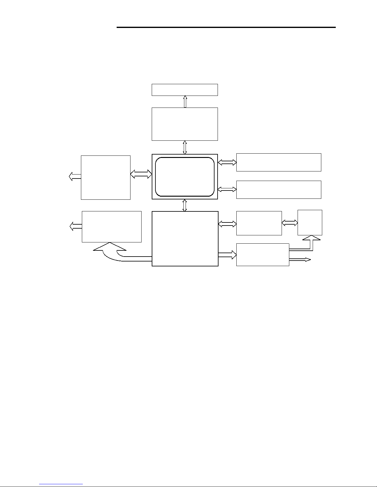
BLOCK DIAGRAM
LCD
IC901
WV2621
LCD Driver + Function
Key
U4, U5 M11L416256SA
SDRAM
U6 W27C020P
EP ROM
U3
LS-188
VCD Decode
U2
TZA1024
Optic system
Mech
Deck
U1 BH6575
Motor driver +
Power control SVCC 3.3V
VIDEO
OUTPUT
U9
SAA7324H/M2B
DSP and DAC System
U12
CS8553
TV ENCODE
U8, U10
BA4510
BH4453
POWER AMPLIFIER
AUDIO
OUTPUT

5
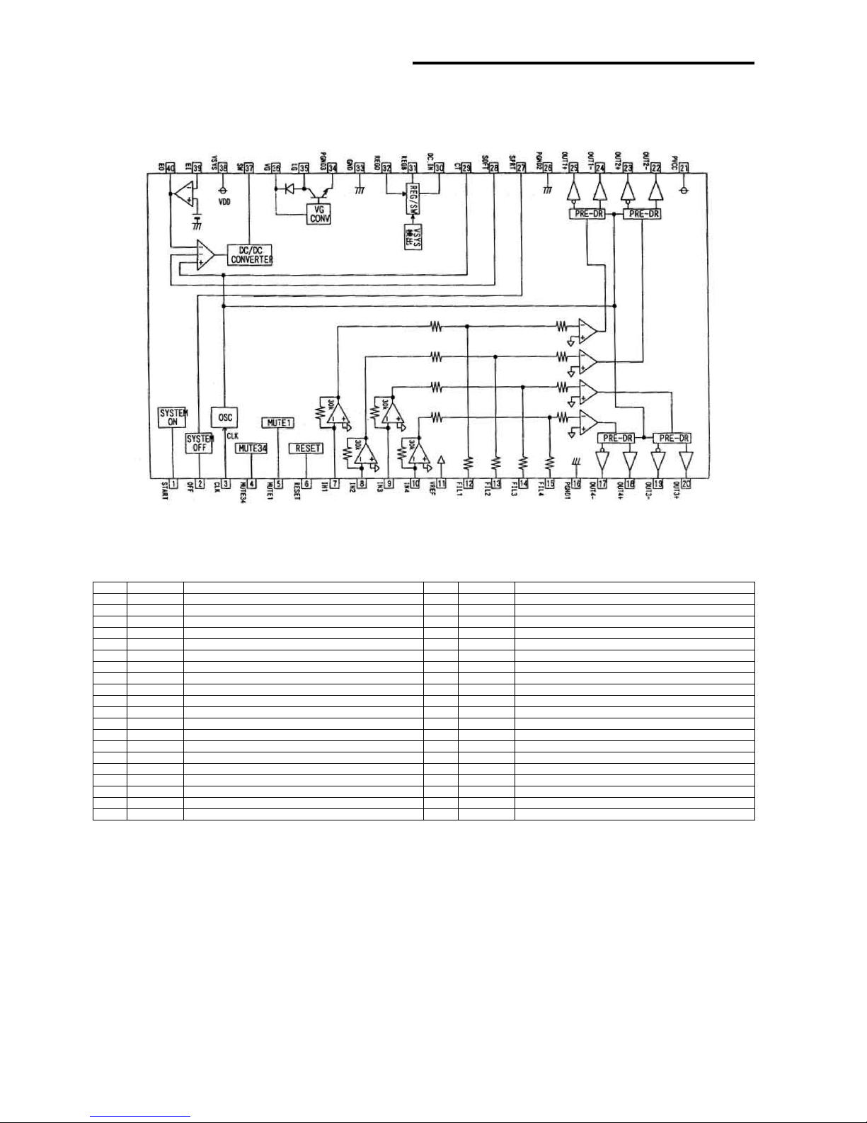
U1 BH6575FV (POWER CONTROLLER)
IC BLOCK DIAGRAM & DESCRIPTION
Symbol Description
OUT4+ CH4 positive output
OUT3- CH3 negative output
OUT3+ CH3 positive output
FIL1 CH1 feedback filter terminal
FIL2 CH2 feedback filter terminal
FIL3 CH3 feedback filter terminal
FIL4 CH4 feedback filter terminal
PGND1 power unit power supply ground terminal 1
OUT4- CH4 negative output
Pin
12
13
14
15
16
17
18
19
20
Symbol Description
SPRT short-circuit protection setting terminal
SOFT soft-start setting terminal
CT Triangular wave output terminal
PVCC H-bridge power supply input terminal
OUT2- CH2 negative output
OUT2+ CH2 positive output
OUT1- CH1 negative output
OUT1+ CH1 positive output
PGND2 power unit power supply ground terminal 2
Pin
21
22
23
24
25
26
27
28
29
START1 DC/DC converter starting terminal
OFF2 DC/DC converter OFF terminal
CLK3 External clock synchronization input terminal
MUTE344 CH3,4 mute terminal
MUTE15 CH1 mute terminal
RESET6 Reset output terminal
IN17 CH1 input terminal
IN28 CH2 input terminal
IN39 CH3 input terminal
IN410 CH4 input terminal
VREF11 Reference power supply input terminal
DC_IN30 AC adapter power supply input terminal
REGB31 Tr driving terminal for regulator
REGO32 Battery power supply input erminal
GND33 Pre-unit power supply input erminal
PGND334 power unit power supply input erminal 3
LG35 Drive coil for boosting VG terminal
VG36 Drive the power-mos circuit power supply input terminal
SW37 Booster transistor drive terminal
VSYS38 Control circuit power supply input terminal
EI39 DC/DC converter error amplifier input terminal
EO40 DC/DC converter error amplifier output terminal

6
MGR517
250
kHz
8
4×
2×
1×
TZA1024
14
3
7
10
1
12
9
V/I
V/I
VDD(L)
VDD
VDD
GND
26
VGAP
MON 4
(1)
DIN 5
CDRW 11
VDD
13
LD
CFIL
PWRON
RGADJ
CMFB
RFFB
RFEQO
EQSEL
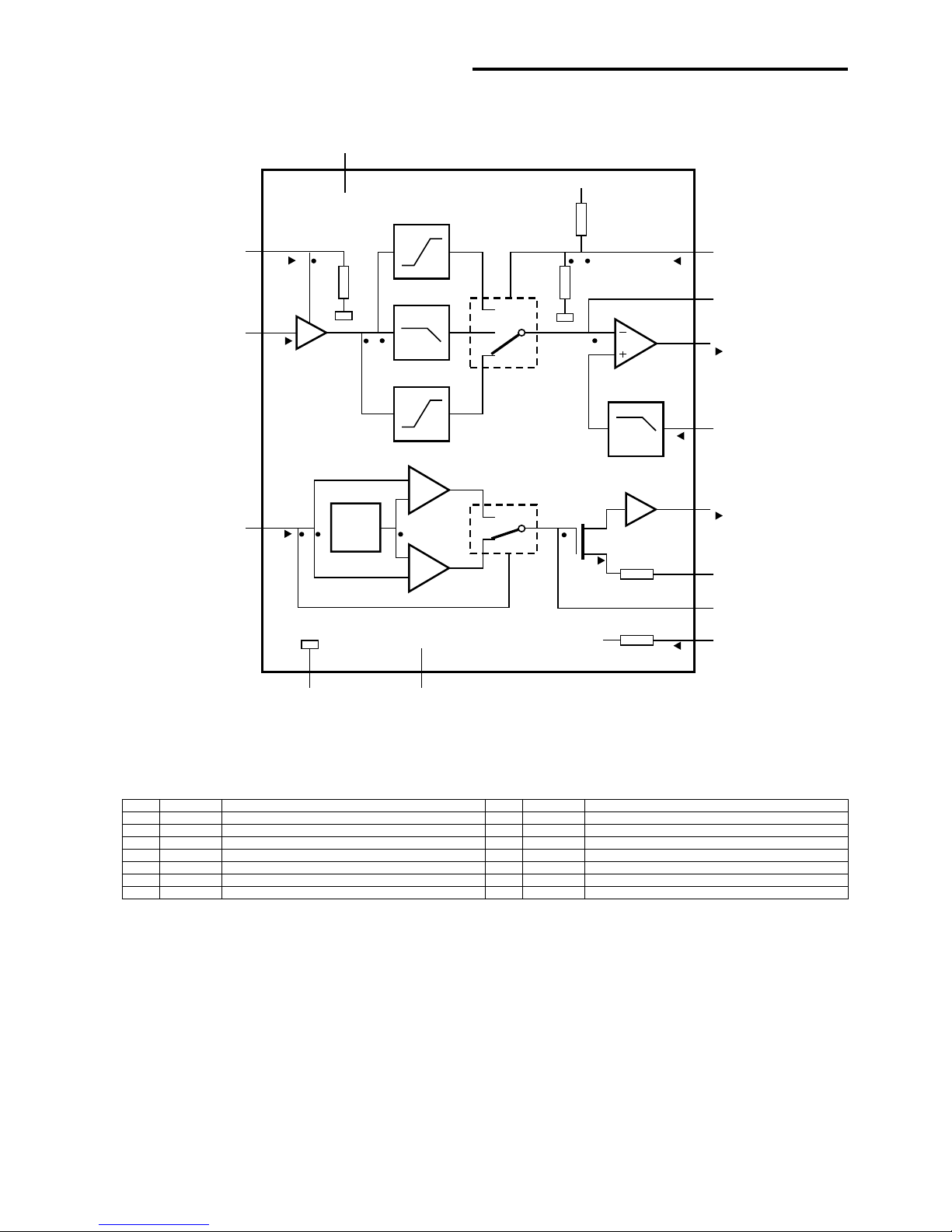
U2 TZA1024 (OPTICAL SYSTEM)
IC BLOCK DIAGRAM & DESCRIPTION
Symbol Description
PWRON power-on select input
LD current output to laser diode
VDD(L) laser supply voltage
CFIL external filter capacitor
MON laser monitor diode input
DIN central diode input
GND ground
Pin
1
2
3
4
5
6
7
Symbol Description
CMFB common mode feedback voltage input
RFFB external RF feedback resistor
Pin
8
9
RFEQO10 RF amplifier output
CDRW11 gain select input for CD-A/V, CD-R/W
EQSEL12 equalizer/speed select input (n=1,2 or 4)
VDD13 supply voltage
RGADJ14 external laser supply gain adjust resistor

7
EMI_A_9
EMI_A_11
EMI_A_10
EMI_D_7
EMI_D_6
EMI_D_5
EMI_D_4
EMI_D_3
EMI_D_2
EMI_D_1
EMI_D_0
EMI_A_0
EMI_A_1
EMI_A_2
EMI_A_3
VDD_IO_00
EMI_A_4
EMI_A_5
VSS_IO_00
EMI_A_6
EMI_A_7
EMI_A_12
EMI_A_15
EMI_A_16
EMI_A_18
I2C_CLK
I2C_DAT
VSS_OSC_0
XTLCLK_I
XTLCLK_O
VDD_OSC_0
TEST_H
RESET_L
HSYNC_L
VSYNC_L
CLK27_O
VDAT_7
VDAT_6
DR_D_7
DR_D_8
VSS_CORE_20
LCAS_L
DR_WE_L
VDD_IO_30
UCAS_L
URAS_L
VDD_CORE_20
LRAS_L
DR_A_8
DR_A_0
DR_A_7
DR_A_1
DR_A_6
VSS_IO_30
DR_A_2
DR_A_5
VSS_CORE_30
DR_A_3
DR_A_4
VDD_CORE_30
EMI_A_17
EMI_A_14
EMI_A_13
EMI_A_8
DR_D_9
DR_D_6
VDD_PLL_0
VSS_PLL_0
DR_D_10
DR_D_5
DR_D_11
DR_D_4
DR_D_12
DR_D_3
VSS_IO_20
DR_D_13
DR_D_2
VDD_IO_20
DR_D_14
DR_D_1
DR_D_15
DR_D_0
CD_C2P0
CD_BCK
CD_LRCK
CD_DATA
IR_IN
GPIO_0
GPIO_1
GPIO_2
GPIO_3
GPIO_4
GPIO_5
GPIO_6
GPIO_7
GPIO_8
GPIO_9
GPIO_10
GPIO_11
GPIO_12
GPIO_13
VSS_IO_10
GPIO_14
GPIO_15
VDD_CORE_10
GPIO_16
GPIO_17
VSS_CORE_10
GPIO_18
GPIO_19
VDD_IO_10
GPIO_20
GPIO_21
GPIO_22
GPIO_23
AUD_DIN
AUD_DOUT
AUD_LRCK
AUD_BCK
AUD_XCK
VDD_CORE_00
VDAT_0
VDAT_1
VSS_CORE_00
VDAT_2
VDAT_3
VDAT_4
VDAT_5
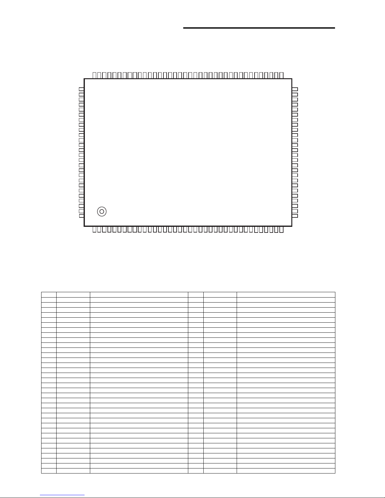
LS188
Luxsonor Inc.
64
63
62
61
60
59
58
57
56
55
54
53
52
51
50
49
48
47
46
45
44
43
42
41
40
39
1
2
3
4
5
6
7
8
9
10
11
12
13
14
15
16
17
18
19
20
21
22
23
24
25
26
27
28
29
30
31
32
33
34
35
36
37
38
103
104
105
106
107
108
109
110
111
112
113
114
115
116
117
118
119
120
121
122
123
124
125
126
127
128
102
101
100
99
98
97
96
95
94
93
92
91
90
89
88
87
86
85
84
83
82
81
80
79
78
77
76
75
74
73
72
71
70
69
68
67
66
65
U3 LS188 (VCD ENCODE)
IC BLOCK DIAGRAM & DESCRIPTION
Symbol Description
EMI_A_18 EMI Adress Bus Outputs 18
EMI_A_9 EMI Adress Bus Outputs 9
EMI_D_0 EMI Data Bus Input 0
EMI_A_0 EMI Adress Bus Outputs 0
EMI_A_1 EMI Adress Bus Outputs 1
EMI_A_2 EMI Adress Bus Outputs 2
Pin
1
11
12
13
14
25
Symbol Description
CLK27_O 27 Mhz Clock output
VDAT_7 Luminance output 7
Pin
36
37
VDAT_638 Luminance output 6
VDAT_539 Luminance output 5
VDAT_440 Luminance output 4
VDAT_341 Luminance output 3
VDAT_242 Luminance output 2
EMI_A_315 EMI Adress Bus Outputs 3
VDD_IO_0016 System I/O power supply
EMI_A_417 EMI Adress Bus Outputs4
EMI_A_518 EMI Adress Bus Outputs 5
VSS_IO_0019 System I/O ground
EMI_A_620 EMI Adress Bus Outputs 6
EMI_A_721 EMI Adress Bus Outputs 7
EMI_A_1222 EMI Adress Bus Outputs 12
EMI_A_1523 EMI Adress Bus Outputs 15
EMI_A_1624 EMI Adress Bus Outputs 16
EMI_A_112 EMI Adress Bus Outputs 11
EMI_A_103 EMI Adress Bus Outputs 10
EMI_D_74 EMI Data Bus Input 7
EMI_D_65 EMI Data Bus Input 6
EMI_D_56 EMI Data Bus Input 5
EMI_D_47 EMI Data Bus Input 4
EMI_D_38 EMI Data Bus Input 3
EMI_D_29 EMI Data Bus Input 2
EMI_D_110 EMI Data Bus Input 1
12C_CLK26 I2C Clock output
12C_DAT27 I2C Clock Bidirectionals
VSS_OSC_028 System OSC ground
XTLCLK_129 Crystal input
XTLCLK_O30 Crystal output
VDD_OSC_031 System OSC power supply
TEST_H32 Test input
RESET_L33 Hardware Reset input
HSYNC_L34 Horizontal sync input
VSYNC_L35 Vertical sync input
VSS_CORE_043 System core ground
VDAT_144 Luminance output 1
VDAT_045 luminance output 0
VSS_CORE_046 System core ground
AUD_XCK47 External audio clock
AUD_BCK48 Audio bit clock output
AUD_LRCK49 Audio left/right clock output
AUD_DOUT50 Audio data output
AUD_DIN51 Audio data input
GPIO_2352 programmable I/O 23
GPIO_2253 programmable I/O 22
GPIO_2154 programmable I/O 21
GPIO_2055 programmable I/O 20
VDD_IO_1056 System I/O power supply
GPIO_1957 Programmable I/O 19
GPIO_1858 programmable I/O 19
VSS_CORE_1059 System core ground
GPIO_1760 programmable I/O 17
GPIO_1661 programmable I/O 16
VDD_CORE_1062 System core power supply
GPIO_1563 programmable I/O 15
GPIO_1464 programmable I/O 14
VSS_IO_1065 System I/O ground
GPIO_1366 programmable I/O 13
GPIO_1267 programmable I/O 12
GPIO_1168 programmable I/O 11
GPIO_1069 programmable I/O 10
GPIO_970 programmable I/O 9

8
U3 LS188 (VCD ENCODE)
IC BLOCK DIAGRAM & DESCRIPTION
Symbol Description
DR_D_10 DRAM Data Bus 10
GPIO_8 programmable I/O 8
CD_C2P0 CD data error flag input
DR_D_0 DRAM Data Bus 0
DR_D_15 DRAM Data Bus 15
DR_D_1 DRAM Data Bus 15
Pin
71
84
85
86
87
98
Symbol DescriptionPin
DR_D_1488 DRAM Data Bus 14
VDD_IO_2089 System I/O power supply
DR_D_290 DRAM Data Bus 2
DR_D_1391 DRAM Data Bus 13
VSS_IO_2092 System I/O ground
DR_D_393 DRAM Data Bus 3
DR_D_1294 DRAM Data Bus 12
DR_D_495 DRAM Data Bus 4
DR_D_1196 DRAM Data Bus 11
DR_D_597 DRAM Data Bus 5
GPIO_673 programmable I/O 6
GPIO_376 programmable I/O 3
GPIO_277 programmable I/O 2
GPIO_178 programmable I/O 1
GPIO_079 programmable I/O 0
IR_IN80 IR input
CD_DATA81 CD serial data input
CD_LRCK82 CD Left/right Clock input
CD_BCK83 CD bit Clock input
VSS_PLL_099 System PLL ground
VDD_PLL_0100 System PLL power supply
DR_D_6101 DRAM Data Bus 6
DR_D_9102 DRAM Data Bus 9
DR_D_7103 DRAM Data Bus 7
DR_D_8104 DRAM Data Bus 8
VSS_CORE_20105 System core ground
GPIO_574 programmable I/O 5
GPIO_475 programmable I/O 4
GPIO_772 programmable I/O 7
LCAS_L106 Lower Column Address Strobe output
DR_WE_L107 Memory Write Enable output
VDD_IO_30108 System I/O power supply
UCAS_L109 Upper Column Address strobe output
URAS_L110 Upper row address strobe output
VSS_CORE_20111 System core ground
LRAS_L112 Lower row address strobe outputs
DR_A_8113 DRAM Address bus outputs 8
DR_A_0114 DRAM Address bus outputs 0
DR_A_7115 DRAM Address bus outputs 7
DR_A_1116 DRAM Address bus outputs 1
DR_A_6117 DRAM Address bus outputs 6
VSS_IO_30118 System I/O ground
DR_A_2119 DRAM Address bus outputs 2
DR_A_5120 DRAM Address bus outputs 5
VSS_CORE_30121 System core ground
DR_A_3122 DRAM Address bus outputs 3
DR_A_4123 DRAM Address bus outputs 4
VDD_CORE_30124 System core power supply
EMI_A_17125 EMI Adress Bus Outputs 17
EMI_A_14126 EMI Adress Bus Outputs 14
EMI_A_13127 EMI Adress Bus Outputs 13
EMI_A_8128 EMI Adress Bus Outputs 8
A6
A5
A4
A3
A2
A1
A0
Q0
5
6
7
8
9
10
11
12
13
Q
1Q
2Q
4Q
5Q
6
1
4
43213
23
13
0A14
A13
A8
A9
OE
A11
Q7
29
28
27
26
25
24
23
22
21
32-pin PLCC
G
N
D
1
51
61
71
81
92
0
1
7
V
c
c
CE
A10
Q5
OE
A10
Q7
Q6
A13
A8
A9
A11
PGM
A17
Q0
A0
A2
A3
A4
A5
A6
A7
A12
A15
A16
A14
A1
Vcc
Vpp
A
1
5
A
1
6
1
2
3
4
5
6
7
8
9
10
11
12
13
14
15
16
30
31
32
25
26
27
28
29
20
21
22
23
24
19
18
17 Q3
Q4
GND
Q2
CE
Q1 Q
3
A7
A
1
2
V
p
p
/
P
G
M
A
32-pin DIP
CONTROL OUTPUT
BUFFER
DECODER CORE
ARRAY
Q0
Q7
.
CE
OE
A0
.
PGM
V
GND
CC
VPP
A17
+
+
1
2
3
4
8
7
6
5
OUT1
– IN1
+ IN1
VEE
VCC
OUT2
– IN2
+ IN2
1ch
2ch
–
–
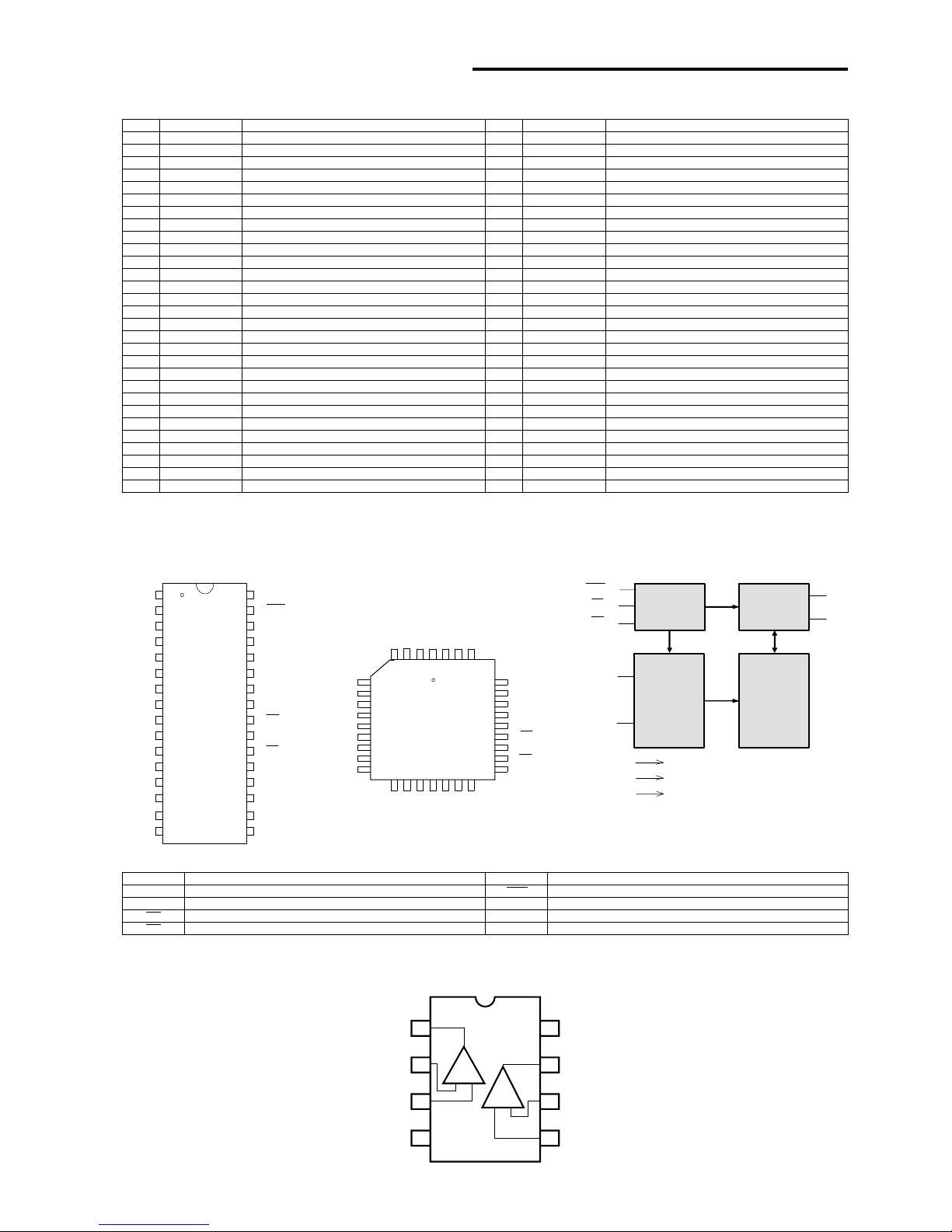
U8 BA4510F (OPERATIONAL AMP)
U6 W27C020 (EPROM)
Symbol Description
A0-A17 Address Inputs
Q0-Q7 Data Inputs/Outputs
CE Chip Enable
OE Output Enable
Symbol Description
PGM Program Enable
VPP Program/Erase Supply Voltage
VCC Power Supply
GND Ground

9
DECODER
MICRO-
CONTROLLER
INTERFACE
VERSATILE PINS
INTERFACE
SUBCODE
PROCESSOR
KILL
PEAK
DETECT
SERIAL DATA
INTERFACE
TIMING
TEST
ADC
Vref
GENERATOR
FRONT-END
DIGITAL
PLL
MOTOR
CONTROL
AUDIO
PROCESSOR
EBU
INTERFACE
ERROR
CORRECTOR
MICROCONTROLLER
INTERFACE
PRE-
PROCESSING
CONTROL
FUNCTION
CONTROL
PART
EFM
DEMODULATOR
SRAM
RAM
ADDRESSER
OUTPUT
STAGES
FLAGS
12
13
7
40
39
41
42
2
1
3
6
25
31
44
24
16
15
26
49
48
47
46
45
43
38
63 34 61 62 32
8 9 10 11 4 14 5 17 33 50 58 52 57
54
55
56
64
59
60
53
51
30
29
28
27
VRIN
Iref
R2
SCL
SDA
RAB
SILD
HFIN
HFREF
ISLICE
TEST1
TEST2
TEST3
SELPLL
CRIN
CROUT
CL16
CL11/4
SBSY
SFSY
SUB
RCK
STATUS
R1
D1 D2 D3 D4 VSSA1
VDDA2 VSSD2
VDDD2(C)
VSSA2
VDDA1 VSSD1 VSSD3
VDDD1(P)
V1 V2/V3 V4 V5 KILL
EF
DATA
WCLK
SCLK
SERIAL DATA
(LOOPBACK)
INTERFACE
37
35
36 SDI
WCLI
SCLI
BITSTREAM
DAC
20
21
18
19 LP
22 RN
23 RP
LN
Vpos
Vneg
DOBM
MOTO2
MOTO1
LDON
SL
FO
RA
CFLG
RESET
SAA7324
MGS174
U9 SAA7324 (DAC SYSTEM)
IC BLOCK DIAGRAM & DESCRIPTION
Symbol Description
D2 unipolar current input 2(central diode signal input)
D3 unipolar current input 3(central diode signal input)
D4 unipolar current input 4(central diode signal input)
HFREF comparator common mode input
VssA1 analog ground 1
VDDA1 analog supply voltage 1
Iref reference current output
VRIN reference voltage for servo ADCs
D1 unipolar current input 1(central diode signal input)
Pin
1
4
5
6
7
8
9
10
11
Symbol Description
V5 versatile output 5
CL11/4 11.2896 or 4.2336 MHZ(for microcontroller)clock output
VSSD2 digital ground 2
VDDD3(C) digital ground 3
MOTO1 motor output 1versatile(3-state)
MOTO2 motor output 2versatile(3-state)
V4 versatile output 4
Pin
49
50
58
59
60
61
62
VSSD133 digital ground 1
V2/V334 versatile l/o:versatile input 2 or versatile output 3(open-drain)
WCLI35 word clock input(for data loopback to DAC)
SDI36 serial data input(for data loopback to DAC)
SCL137 serial bit clock input (for data loopback to DAC)
RESET38 power-on reset input(active low)
SDA39 microcontroller interface data l/o line (l2c-busopen-drain output)
SCL40 microcontroller interface clock line input (l2c-bus)
RAB41
microcontroller interface R/W and load control line input(4-wire bus mode)
SILD42
microcontroller interface R/W and load control line input(4-wire bus mode)
STATUS43
servo interrupt repuest line/decoder status register output(open-drain)
TEST344 test control input 3(this pin shoud be tied LOW)
RCK45 subcode clock input
SUB46 P-to-W subcode bit 3-states output(3-state)
SFSY47 subcode frame sync output(3-state)
SBSY48 subcode block sync output(3-state)
DOBM51 bi-phase mark output(externally buffered3-state)
VDDD1(P)52 digital supply voltage 1 for periphery
CFLG53 correction flag output(open-drain)
RA54 radial actuator output
FO55 focus actuator output
SL56 sledge control output
VDDD2(C)
57 digital supply voltage 2 for core
R112 unipolar current input 1(satellite diode signal input)
R213 unipolar current input 2(satellite diode signal input)
VSSA214 analog ground 2
CROUT15 crystal/resonator output
CRIN16 crystal/resonator input
VDDA217 analog supply voltage 2
LN18 DAC left channel differential negative output
LP19 DAC left channel differential positive output
Vneg20 DAC negative reference input
Vpos21 DAC positive reference input
RN22 DAC right channel differential negative output
RP23 DAC right channel differential positive output
SELPLL24 selects whether internal clock multiplier PLL is used
TEST125 test control input 1 (this pin should be tied low)
CL1626 16.9344 MHZ system clock output
DATA27 serial d4(1)data output (3-state)
WCLK28 word clock output(3-state)
SCLK29 serial bit clock output(3-state)
EF30 C2 error flag output(3-state)
TEST231 test control input 2(this pin should be tied LOW)
KILL32 kill output (programmableopen-drain)
HFIN2 coparator signal input
3 ISLICE current feedback output fron data slicer
V163 versatile input 1
LDON64 laser drive on output(open-drain)

10
VIDEO-TIMING
CONTROLLER
SUB-CARRIER
GENERATION SINE-TABLE
SERIAL
TO
PARALLEL
4:2:2 to
4:4:4
INTER-
u-FILTER
v-FILTER
y-FILTER
POLATION
H, V-SYNC
CLK_27
SLEEP
P[7:0]
MODE[3:0]
SVIDEO
MASTER
CBSWAP
COLOR-BURST
&
MODULATION
&
MIXER
CVBS/Y
DAC-
MAPPING
VBIAS VREF_O FSADJUST COMP
DAC
U10 BH4453F (POWER AMP)
U12 CS8553 (TV ENCODE)
IC BLOCK DIAGRAM & DESCRIPTION
Symbol Description
OUT1 Output 1 terminal
Pin
1
Symbol DescriptionPin
IN13 Input 1 terminal
IN25 Input 2 terminal
BIAS6 BIAS terminal
GND4 Ground
MUTE2 Mute control terminal (mute = low)
OUT27 output 2 terminal
VCC8 Power supply
Symbol Description
HSYNC Horizonta sync,output in master mode or input in slave
mode,is synchronized by CLKtoo.
Pin
1
Symbol DescriptionPin
AGND3 Analog ground
CVBS/Y4 Composite output or luminance (with blanking and sync)
NC/VSS2 No connection in PLCC.Analog ground in TQFP
VSYNC32 Vertical sync,output in master mode or input in slave mode,
is synchronized by CLK.
P[7:0]21
YCbCr pixel inputs (TTL compatible).Also,synchronized by
CLK with respect to the incoming HSYNC timing,the higher
index corresponds to a greater significance.
P[7:1]22
YCbCr pixel inputs (TTL compatible).Also,synchronized by
CLK with respect to the incoming HSYNC timing,the higher
index corresponds to a greater significance.
P[7:2]23
YCbCr pixel inputs (TTL compatible).Also,synchronized by
CLK with respect to the incoming HSYNC timing,the higher
index corresponds to a greater significance.
P[7:3]24
YCbCr pixel inputs (TTL compatible).Also,synchronized by
CLK with respect to the incoming HSYNC timing,the higher
index corresponds to a greater significance.
P[7:4]25
YCbCr pixel inputs (TTL compatible).Also,synchronized by
CLK with respect to the incoming HSYNC timing,the higher
index corresponds to a greater significance.
P[7:5]26
YCbCr pixel inputs (TTL compatible).Also,synchronized by
CLK with respect to the incoming HSYNC timing,the higher
index corresponds to a greater significance.
P[7:6]27
YCbCr pixel inputs (TTL compatible).Also,synchronized by
CLK with respect to the incoming HSYNC timing,the higher
index corresponds to a greater significance.
P[7:7]28
YCbCr pixel inputs (TTL compatible).Also,synchronized by
CLK with respect to the incoming HSYNC timing,the higher
index corresponds to a greater significance.
CLKI29 Pixel clock,27MHZ,twice the Y sample rate
VDD31 Digital power
FSADJUST5
Full scale adjust control pin. A resistor is connected to GND.
Used to control the fullscale output current on analog
outputs.
COMP6 Compensation pin. A 0.1uF capacitor is used to bypass this
pin to VCC.
VAA7 Analog power
VREFO8 Voltage reference output ,typically 1.2V,may be used to
connect to VREFI input
VREFI/VRDAC9
Voltage reference input ,typically 1.235V. A 0.11uF capacitor
must be used to decouple this input to GND. DAC current
switch reference input ,connect to Vrefo output
VBIAS10 DAC bias voltage, 0.7 v less than COMP signal
NC11 No connection in PLCC.Analog ground in TQFP
AGND12 Analog ground
SLEEP13 1:power down,reset 0:normal operation
SVIDEO14 00:00 composite output same signal on both Y,C channels,
01:00 s-video output,Y,C channels
CBSWAP15 0:Normal Cr,Cb sequence .1:swaps Cr ,Cb sequence
MASTER16 in 0:slave mode,h and v sync are inputs. 01:00 master mode,
h and v sync are outputs.
MD[3:0]17 Configuration inputs
MD[3:0]18 Configuration inputs
MD[3:0]20 Configuration inputs
MD[3:0]19 Configuration inputs
GND30 Digital ground

11
WIRING CONNECTION
MAIN PCB
KEY PCBCD MECHANISM
LCD DISPLAY DESCRIPTION

12
VOLTAGE OF IC & TRANSISTOR
Q8 2SD2150 Q10 DTC114TUA
Q2 2SD2150 Q3 2SD2150
B EBCE
0.15 0 3 3.7 3.4
U3 LS188 (VCD ENCODE)
U2 TZA1024 (OPTICAL SYSTEM)
PIN 12345678910 11 12 13 14
1.8 3.2 0.8 0.2 0.7 0 1.7 1.5 0.8 1.7 0 3.3 3.2 1.1
PIN 12345678910 11 12 13 14 15
PLAY VCD 1 2 1.3 0.4 0 0.7 1.5 0.9 0.5 0.5 0.5 0.8 0.8 0.8 0.8
(V)
PLAY CD 1 2 1.3 0.4 0 0.7 1.5 0.9 0.5 0.5 0.5 0.8 0.8 0.8 0.8
PLAY MP3 1 2 1.3 0.4 0 0.7 1.5 0.9 0.5 0.5 0.5 0.8 0.8 0.8 0.8
PIN 17 18 19 20 21 22 23 24 25 26 27 28 29 30 31
PLAY CD 0.8 0.8 0 1.2 1.7 2 00002.62.6003.3
PLAY MP3 0.8 0.8 0 1.2 1.7 2 0 0 0 2.6 2.6 0 1.5 0 3.3
PLAY VCD 0.8 0.8 0 1.2 1.7 2 0 0 0 2.6 2.6 0 1.5 0 3.3
PIN 33 34 35 36 37 38 39 40 41 42 43 44 45 46 47
PLAY CD 3.3 2.1 2.1 3.3 3.3 0 00000002.11.8
PLAYMP33.32.12.13.33.3003.3000002.11.8
PLAYVCD3.32.12.13.33.3003.3000002.11.8
PIN 49 50 51 52 53 54 55 56 57 58 59 60 61 62 63
PLAY CD 1.7 1.7 0.6 3.3 3.3 2.6 2.6 3.3 3.3 3.3 0 2.6 2.6 2.2 0.6
PLAY MP3 1.7 1.7 0.6 3.3 3.3 2.6 2.6 3.3 3.3 3.3 0 2.6 2.6 2.2 0.6
PLAY VCD 1.7 1.7 0.6 0 3.3 2.6 2.6 3.3 3.3 3.3 0 2.6 2.6 2.2 0.6
PIN 65 66 67 68 69 70 71 72 73 74 75 76 77 78 79
PLAY CD 0 2.8 3.3 3.3 2.8 3.3 0 0 3.3 3.3 3.3 3.3 0 2.8 3.3
PLAY MP3 0 3.3 3.3 3.3 2.8 3.3 0 0 3.3 3.3 3.3 3.3 0 2.8 3.3
PLAY VCD 0 3.3 3.3 3.3 2.8 3.3 0 0 3.3 3.3 3.3 3.3 0 2.8 3.3
PIN 81 82 83 84 85 86 87 88 89 90 91 92 93 94 95
PLAY CD 1.7 1.7 1.7 0 1.6 1.6 1.6 1.6 3.3 1.6 1.7 0 0.6 0.6 0.6
PLAY MP3 1.7 1.7 1.7 1.6 1.6 1.6 1.6 3.3 3.3 3.3 1.7 0 0 0.6 1.2
PLAY VCD 1.7 1.7 1.7 0 1.6 1.6 1.6 3.3 3.3 3.3 1.7 0 0 0.6 1.2
PIN 97 98 99 100 101 102 103 104 105 106 107 108 109 110 111
PLAY CD 0.6 0.6 0 2.1 0.6 1.2 0.6 1.7 0 3.3 3.3 3.3 3.3 3.3 2.1
PLAY MP3 0.6 0.6 0 2.1 0.6 1.2 0.6 1.7 0 3.3 3.3 3.3 3.3 3.3 2.1
PLAY VCD 0.6 0.6 0 2.1 0.6 1.2 0.6 1.7 0 3.3 3.3 3.3 3.3 3.3 2.1
PIN 113 114 115 116 117 118 119 120 121 122 123 124 125 126 127
PLAY CD 1.2 2.5 1.1 1.8 1.2 0 2.3 1.2 0 2.9 1.3 2.1 1.7 3.3 0
PLAY MP3 2.2 2.5 1.1 1.8 1.2 0 2.3 1.2 0 2.9 1.3 2.1 1.7 3.3 0
PLAY VCD 2.2 2.5 1.1 1.8 1.2 0 2.3 1.2 0 2.9 1.3 2.1 1.7 3.3 0
U4/U5 M11L416256SA (SDRAM)
PIN 12345678910 11 12 13 14 15
3.3 1.7 1.7 1.7 1.7 3.3 1.7 1.7 1.7 1.7 0 0 3.3 3.3 0
PIN 17 18 19 20 21 22 23 24 25 26 27 28 29 30 31
1.31.133.300000003.33.301.7
PIN 33 34 35 36 37 38 39 40
1.7 1.7 0 1.7 1.7 1.7 1.7 0
U6 W27C020 (EPROM)
PIN 12345678910 11 12 13 14 15
1.5 1.3 1.3 1.3 1.3 1.3 1.3 1.3 0.9 0.9 0.9 0 0 0.7 0.7
PIN 17 18 19 20 21 22 23 24 25 26 27 28 29 30 31
0.8 0 2.8 0 2 2.6 1.6 1.6 3 1.5 3.3 3.3 3.3 0 0
U8 BA4510F (OPERATIONAL AMP)
PIN 12345678
1.4 1.5 1.5 0 1.5 1.5 1.5 3.3
U10 BH4453F (POWER AMP)
PIN 12345678
1.4 2.6 1.4 0 1.4 1.4 1.4 3.3
(V)
(v)
U1 BH6575FV (POWER CONTROLLER)
PIN 12345678910 11 12 13 14 15
3.3 3.3 0 1.6 0 3.3 1.5 1.5 1.5 1.5 1.5 1.5 1.5 1.5 1.5
PIN 17 18 19 20 21 22 23 24 25 26 27 28 29 30 31
0.50003.9000000.041.10.603.2
PIN 33 34 35 36 37 38 39 40
0 0 3.8 5.9 0.2 3.3 0.9 0.4
(V)
16
0
32
3.8
(V)
16
3.3
3.3
3.3
32
0
0
0
48
1.7
1.7
1.7
64
0
3.1
3.1
80
3.3
3.3
3.3
96
0.6
0.6
0.6
112
3.1
3.1
3.1
128
1.6
1.6
1.6
(V)
16
1.6
32
1.7
U12 CS8553 (TV ENCODE)
PIN 12345678910 11 12 13 14 15
PLAY CD 0 2.1 2.1 0.9 0.9 0 0.7 0 3.3 0 0 2.1 0 3.3 2.1
PLAY MP3 0 2.1 2.1 0.9 0.9 0 0.7 0 3.3 0 0 2.1 0 3.3 2.1
PLAYVCD00.72.10.90.900.700002.103.32.1
PIN 17 18 19 20 21 22 23 24 25 26 27 28 29 30 31
PLAY CD 00003.30003.302.12.12.100
(V)
16
0
0
0
32
0
U9 SAA7324 (DAC SYSTEM)
PIN 12345678910 11 12 13 14 15
1.5 1.7 1.7 0 3.3 1.2 1.5 1.5 1.5 1.5 1.5 1.5 1.5 0 1.7
PIN 17 18 19 20 21 22 23 24 25 26 27 28 29 30 31
3.3 1.5 1.6 0 3.3 1.5 1.6 3.3 0 1.8 1.6 1.6 1.6 0 0
PIN 33 34 35 36 37 38 39 40 41 42 43 44 45 46 47
0 0 1.6 1.6 1.6 2.3 3.3 3.3 3.3 0 0 0 0.5 0 1.9
(V)
16
1.6
32
0
48
0.5
(V)
16
0.6
32
1.7
(V)
Q4 2SD2150 Q5 DTA144TUA Q6 DTC114TUA Q7 2SB1132
BCEBCEBCEBCE
4.4 5.5 3.3 0 3.3 3.3 0 0.1 0 3.1 2.1 3.8
Q11 DTC114TUA
1.9 1.4 3.8 0 0 3.8 3.3 3.3
C
3.7
3.1
BCEBCEBCE
PLAYMP300003.30003.302.12.12.1000
PLAY VCD 1.2 1.1 1.1 0 0 1.4 0 3.3 1.5 0 2.1 2.1 2.1 0 0.2 0.7
PIN 49 50 51 52 53 54 55 56 57 58 59 60 61 62 63 64
0.6 0 1.6 3.3 0 1.5 1.2 0 3.3 0 1.7 1.6 1.5 3.3 3.3 1.7

13
SCHEMATIC DIAGRAM
MAIN PCB (1/2)

14
SCHEMATIC DIAGRAM
MAIN PCB (1/2)
TO KEY PCB

15
SCHEMATIC DIAGRAM
MAIN PCB (2/2)

16
SCHEMATIC DIAGRAM
MAIN PCB (2/2)

17
CN901
SCHEMATIC DIAGRAM
KEY PCB

18
SW2
J2
J3
WIRING DIAGRAM (MAIN PCB)
TOP VIEW

19
WIRING DIAGRAM (MAIN PCB)
BOTTOM VIEW
Table of contents
Other Sanyo CD Player manuals

Sanyo
Sanyo MCD-S735F User manual

Sanyo
Sanyo MAX-5000 User manual

Sanyo
Sanyo CDP-4000 User manual

Sanyo
Sanyo MCD-ZX540F User manual

Sanyo
Sanyo CDP-M303 User manual

Sanyo
Sanyo CDP-355 User manual

Sanyo
Sanyo MCD-Z16F User manual

Sanyo
Sanyo PH-DS280 User manual

Sanyo
Sanyo MCD-Z260F User manual

Sanyo
Sanyo CDP-360 User manual

Sanyo
Sanyo CP10 User manual

Sanyo
Sanyo FXD-C222 User manual

Sanyo
Sanyo CDP-4000 User manual

Sanyo
Sanyo CDP-150 User manual

Sanyo
Sanyo CDP-990 User manual

Sanyo
Sanyo MCD-XP400 User manual

Sanyo
Sanyo MCD-XP630 User manual

Sanyo
Sanyo CDP-S4900 XE User manual

Sanyo
Sanyo CDP-970 User manual

Sanyo
Sanyo CM-200 User manual