Schlage HandPunch F Series User manual

Title
Number Revision
Created By
Creation Date
EC Number
Revision Description:
Allegion
Copyright © 2015
Material Edited By Approved By Release Date
Revision History
Additional Notes: A B C D E F
Notes
Software: Illustrator CS6
Activity
3899 Hancock Expwy
Security, CO 80911
20156 062621
White Paper
F > Allegion Rebranding
062621 05-14-2015R. Byun M. Roberts
F-Series Hand Punch Modem Instruction
J. Ellis
08-29-11 70200-0013 F
11.000
17.000
FRONT FRONT
8.500
BEGINNING SHEET FOLDED SHEET
1. printed two sides
2. printed black
3. tolerance: ± .13
4. see sheet 2 for artwork
5. printed in country may vary
6. drawings not to scale
11.000
2 sheets, 1 fold, side stitched
F Series HandPunch Modem
Installation Instructions
70200-0013
Periodically, enhancements to the HandKey or HandPunch are introduced that offer added functionality and performance. Should it be necessary
to incorporate the enhancements into the F Series circuit board (HP-2000, HP-3000, HP-4000, HK-2 and HK-CR), use the following procedures.
CAUTION: This procedure requires erasing the existing hand templates. Save the existing hand templates before proceeding.
1. Unlock the reader and rotate.
2. Disconnect the power supply from the board.
3. Remove and tag all external connections to make correct re-attachment.
CAUTION: If the unit is equipped with an optional battery backup, remove the J7 jumper before proceeding. See figure 9.
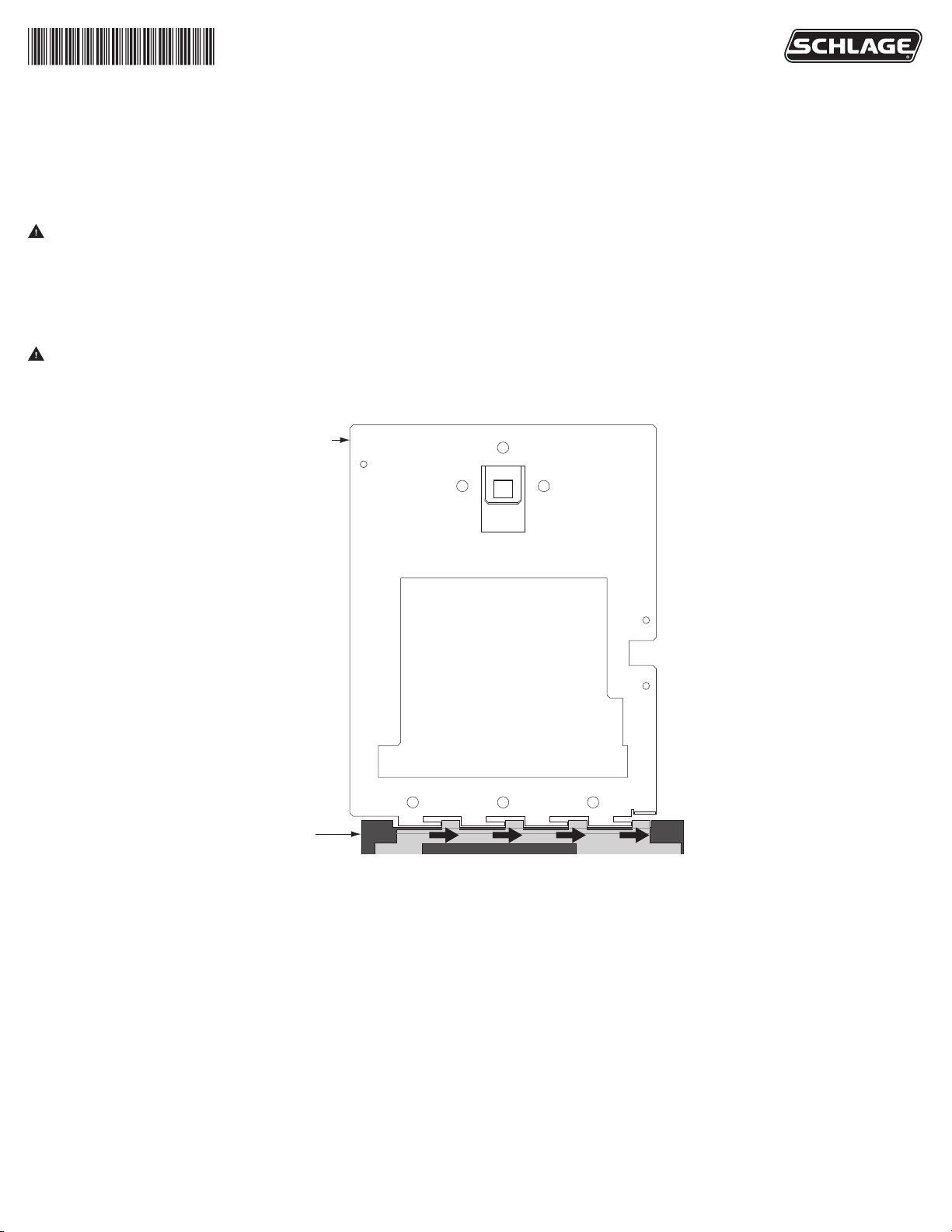
4. Remove HandReader from wall by sliding it to the right, away from the wall mount. See figure 1 below.
Reader
Wall Mount
Figure 1
2
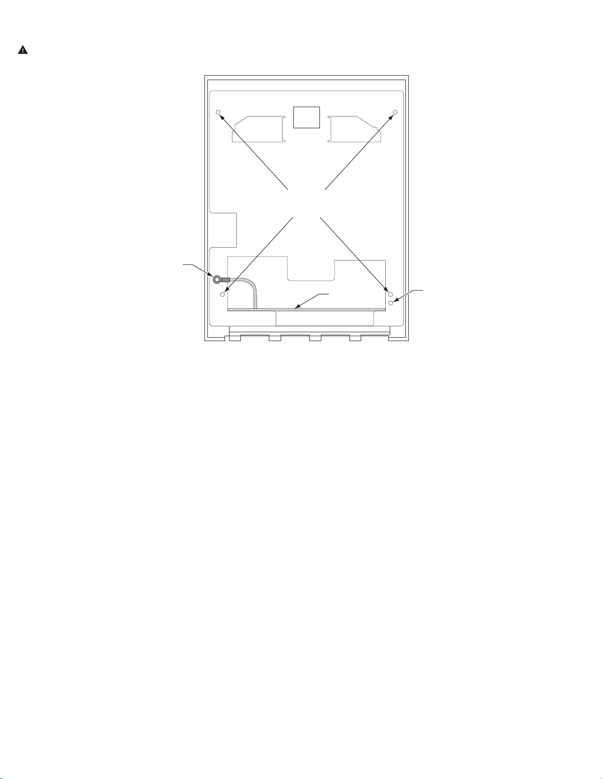
5. Set the reader on a firm surface such as a table. Remove the four screws that secure the back plate to the HandReader. Remove the
grounding screw and/or ground lug (if present). See figure 2 below.
CAUTION: Before removing back plate of reader, wear a grounding wrist strap to help aid in protecting the circuit board from any
ESD damage that might occur from improper handling.
Back
Plate
Screws
Grounding
Screw
Ground Lug,
if present
Main Circuit
Board
See Caution
Above
Figure 2
6. Remove the back plate.

3
7. Locate the cable that runs from the top panel circuit board to the main circuit board. Disconnect this cable from J9 on the main circuit
board. See “1” on figure 3. To remove the J9 connector on the main circuit board (lower board), depress the retaining clip on the
connector and pull upwards. See figure 4 below.
Main Circuit Board
1
J9
Figure 3
Press to Release
Figure 4
4
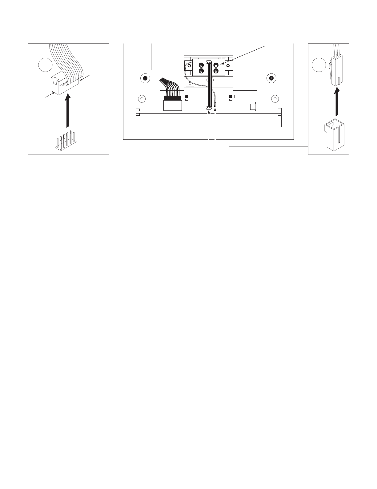
8. Carefully slide the main circuit board out until the ribbon cable between the camera assembly and J2 on the main circuit board is
accessible. First, disconnect the J5 connector from the main board. To remove, depress the retaining clip on the J5 connector and pull
upwards. See “2” on figure 5 below. Next, remove the ribbon cable from J2 by gently pulling up on this cable, being careful not to pull
down as damage may occur to the camera assembly. See “3” on figure 5 below.
Camera
Assembly
J2 J5
3
Grasp
here to
lift
Grasp
here to
lift
2
Figure 5
9. Carefully remove the main circuit board by sliding it free from the chassis.
5
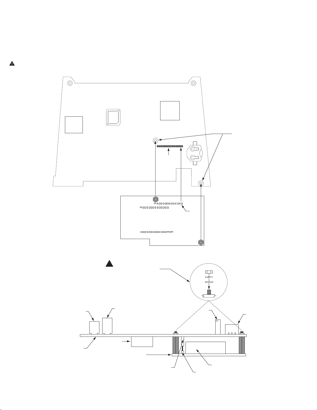
10. Install the modem PCB onto the main PCB. See figures 6 and 7 below.
a. Align P1 on the modem PCB with J10 on the underside of the main PCB.
b. Insert the P1 pins into the J10 socket. If done correctly, the two standoffs on the modem PCB should insert through the
mounting holes in the main PCB.
c. Turn the PCB’s over so that the main circuit board is on top of the modem PCB. Secure the modem PCB to the main PCB by
adding the provided flat washers, split washers, and nuts onto the standoff(s). Tighten the nuts using a C/zn” nut driver.
CAUTION: Torque the 4-40 nuts to 4.5 – 5.5 in. lbs. (.51 -.62 Nm). Excessive torque may damage the circuit boards. After installing
the modem, inspect for warped modem PCB or main PCB.
J10
Modem PCB
(Underside View)
P1
Modem PCB
Mounting Holes
Figure 6
Side View
J9
P1
Modem
J10
Modem PCB
Main PCB
CAUTION: Do not over
torque the nuts. See
step 10 for limits.
!
J4
T1
C3
C1
Figure 7

6
11. Carefully slide circuit board back into the chassis using the circuit board guides to locate the circuit board correctly. See figure 8 below.
Circuit Board
Guides
Figure 8
12. Being careful to align all pins, attach the camera cable to J2 on the main circuit board.
13. Plug in the J5 connector.

7
14. Locate the cable that runs from the top panel circuit board to the main circuit board. Connect this cable to J9 on the main circuit board.
See figure 10 for cable routing.
15. If not already removed, remove the J7 jumper from the main PCB. See figure 9 below.
J7
Out
J7
In
Figure 9
CAUTION: If there is a ground strap on the main board, do not allow the ground strap to touch the J7 jumper. Failure to do so will
cause permanent damage to the main circuit board and will not be considered a warranty repair.

8
Main Circuit Board
Battery
J4
J9
Figure 10
16. Reinstall the back plate onto the chassis. Reinstall grounding screw and/or ground lug. If a ground lug is present, do not allow it to
come into contact with J7.
17. Secure the back plate with the four screws removed in step 5.
18. Line up the slots at the bottom of the reader’s back with the four hinge pins at the bottom of the wall mount. Slide the reader to the left
so the pins go in the slots. This fastens the reader to the wall and wall mount and forms a hinge.
19. Reconnect all external connections removed in step 3.
20. Power up the unit and reinstall the J7 jumper (if applicable).
21. Secure unit to wall mount with key. Upgrade is completed.
© Allegion 2015
Printed in U.S.A.
70200-0013 Rev. 05/15-f
Customer Service
1-877-671-7011 www.allegion.com
Table of contents
Other Schlage Modem manuals


Popular Modem manuals by other brands


iiNet
iiNet BOB2 user manual

US Robotics
US Robotics USR5610B installation guide

Westell Technologies
Westell Technologies WIRESPEED B90-36R305 Installation and user guide

Embedded Planet
Embedded Planet epConnected Asset Product user manual

Cradlepoint
Cradlepoint MBR95 quick start guide

Buenoptic
Buenoptic HFB Series user manual