SG Micro SGM41562A User manual

SGM41562A/SGM41562B
500mA Single-Cell Li-Ion Battery Charger
with Power Path Management
SG Micro Corp
www.sg-micro.com
JANUARY 2022 - REV. A. 1
GENERAL DESCRIPTION
The SGM41562A and SGM41562B are highly integrated, I2C
programmable, single-cell Li-Ion or Li-polymer battery chargers
with system power path management. They are specifically
designed for portable applications requiring minimum board
space and small external components. The charging profile
includes pre-charge, constant-current and constant-voltage
phases. Several safety and protection features are included
such as built-in safe charge timer to set maximum duration of
charge and pre-charge, input voltage and current monitoring,
internal (junction) and external (battery) temperature monitoring,
input current limiting and load current limiting. SGM41562A
can charge with a wide input voltage range of up to 18V
compared to the SGM41562B which has 5.75V charging
range, but the rest of their functions are the same.
The SGM41562A/B has 3 power ports: input power port (IN),
battery port (BAT) and system or load port (SYS). The system
is powered from the input whenever it is available. Input is
typically a USB power source. If the input source is weak or
removed, power source for the system will automatically switch
to the battery. The voltage and currents from input and
battery as power sources are continuously monitored to
prevent battery damage due to excessive currents or
over-discharge.
I2C serial interface is used to program the device functions
and parameters or to read its status. 12 read/write or read only
8-bit registers (REG00 to REG0B) are accessible. A watchdog
protection feature is also included. If this feature is enabled
and there is no in time read/write activity or signal from the
host, the device will reset the charging parameters to their
defaults and recycles power to the system (turn off/on) that
may reset the host.
The SGM41562A is capable of charging with input voltages
as high as 18V but with higher input voltages, the chip
temperature can easily rise up and thermal protection may
stop charging if proper cooling is not considered. The
SGM41562B goes into voltage protection state if VIN > 6V.
The input changes are continuously monitored and a system
power recycle (SYS) may occur if the system does not
response to the input toggles.
The SGM41562A/B is available in a Green WLCSP-1.52×1.52-9B
package. Device functionality and protection features are
assured in the ambient temperature range from -40℃to
+125℃. Charging parameters are guaranteed in 0℃to +55℃.
FEATURES
●Fully Autonomous Charger for Single-Cell Li-Ion and
Li-Polymer Battery
●±0.6% Charging Voltage Accuracy
●21V Maximum Input Voltage Rating with Over-Voltage
Protection
●18V Maximum Operating Voltage (SGM41562A)
●5.75V Maximum Operating Voltage (SGM41562B)
●I2C Interface for Parameters Setting/Status Reporting
●Fully Integrated Power Switches
●No External Blocking Diode Required
●Built-in Robust Charge Protections Including Battery
Temperature Monitor and Programmable Timer
●Battery or PCB Over-Temperature Protection
●Built-in Battery Disconnection Function
●System Reset Function
●Thermal Limit Regulation on Chip
●Available in a Green WLCSP-1.52×1.52-9B Package
APPLICATIONS
Wearable Devices
IoT Gadgets
TYPICAL APPLICATION
USB
Port
Host
4.7μF
SGM41562B
Qswitch
10μF
4.7μF
IN
VDD
nINT
SDA
SCL
BAT
NTC
SYS
GND
System Load
VDD
Li-Ion
Battery
Pack
Qrvs
Qbypass
1μF
Figure 1. Typical Application Circuit
SGM41562A 500mA Single-Cell Li-Ion Battery Charger
SGM41562B with Power Path Management
2
JANUARY 2022
SG Micro Corp
www.sg-micro.com
PACKAGE/ORDERING INFORMATION
MODEL PACKAGE
DESCRIPTION
SPECIFIED
TEMPERATURE
RANGE
ORDERING
NUMBER
PACKAGE
MARKING
PACKING
OPTION
SGM41562A WLCSP-1.52×1.52-9B -40℃to +125℃SGM41562AXG/TR
XXXXX
RD0
Tape and Reel, 3000
SGM41562B WLCSP-1.52×1.52-9B -40℃to +125℃SGM41562BXG/TR
XXXXX
RD1
Tape and Reel, 3000
MARKING INFORMATION
NOTE: XXXXX = Date Code, Trace Code and Vendor Code.
Trace Code
Vendor Code
Date Code - Year
X XXX X
Serial Number
YY
Y
Green (RoHS & HSF): SG Micro Corp defines "Green" to mean Pb-Free (RoHS compatible) and free of halogen substances. If
you have additional comments or questions, please contact your SGMICRO representative directly.
ABSOLUTE MAXIMUM RATINGS
IN ....................................................................... -0.3V to 21V
SYS ........................................-0.3V to 5.3V (5.5V for 500μs)
All Other Pins to GND.......................................... -0.3V to 6V
IINCLAMP ............................................................................ 5mA
Package Thermal Resistance
WLCSP-1.52×1.52-9B, θJA ........................................ 95℃/W
Junction Temperature.................................................+150℃
Storage Temperature Range ....................... -65℃to +150℃
Lead Temperature (Soldering, 10s) ............................+260℃
ESD Susceptibility
HBM............................................................................. 3000V
CDM ............................................................................ 1000V
RECOMMENDED OPERATING CONDITIONS
Supply Voltage, VIN ... 4.35V to 18V (SGM41562A, Charging)
................................. 4.35V to 5.5V (SGM41562B, Charging)
(Over-Voltage Protection State, Continuous) ............... 19V
IIN ...................................................................... Up to 500mA
IBAT ........................................................................ Up to 3.2A
ICHG ................................................................... Up to 456mA
VBAT_REG ............................................................ Up to 4.545V
Operating Junction Temperature Range .......-40℃to +125℃
OVERSTRESS CAUTION
Stresses beyond those listed in Absolute Maximum Ratings
may cause permanent damage to the device. Exposure
to
absolute maximum rating conditions for extended periods
may affect reliability. Functional operation of the device at any
conditions beyond those indicated in the Recommended
Operating Conditions section
is not implied.
ESD SENSITIVITY CAUTION
This integrated circuit can be damaged if ESD protections are
not considered carefully. SGMICRO recommends that all
integrated circuits be handled with appropriate precautions.
Failure
to observe proper handling
and installation procedures
can cause damage. ESD damage can range from subtle
performance
degradation to
complete device failure. Precision
integrated circuits may be more susceptible to damage
because even small parametric changes could cause the
device not to meet the published specifications.
DISCLAIMER
SG Micro Corp reserves the right to make any change in
circuit
design, or specifications
without prior notice.

SGM41562A 500mA Single-Cell Li-Ion Battery Charger
SGM41562B with Power Path Management
3
JANUARY 2022
SG Micro Corp
www.sg-micro.com
PIN CONFIGURATION
(TOP VIEW)
IN SYS BAT
NTC nINT VDD
SDA SCL GND
1 2 3
A
B
C
WLCSP-1.52×1.52-9B
PIN DESCRIPTION
PIN NAME TYPE (1) FUNCTION
A1 IN P Input Power Pin. Place a minimum 2.2μ
F ceramic capacitor between IN pin and GND pin as close as
possible to these pins.
A2 SYS P
System Power Supply Output. Place a ceramic capacitor between SYS pin and GND pin as close as
possible to these pins.
A3 BAT P
Battery Positive Terminal Connection Pin. Place a ceramic capacitor between BAT pin and GND pin
as close as possible to the device. Connect the negative battery terminal to power GND.
B1 NTC AIO
Battery Temperature Sense Input. Connect a negative te
mperature coefficient thermistor between this
pin and GND pin. NTC is usually placed in touch with battery pack. Hot-
cold temperature window can be
programmed by a resistor divider network placed between VDD to NTC to GND pins. Charging will
suspend if NTC function is enabled and NTC pin voltage goes out of the VHOT and VCOLD range.
B2 nINT DIO
Interrupt Output Pin. The nINT pin
can send a charging status and fault interrupt signal to the host.
nINT is also used to disconnect the system from the battery. Pull nINT pin from high to low for >
tRST_DGL (16s default). The battery FET turns off and turns on again automatically after > tRST_DUR
(4s
default) regardless of the nINT state. Both tRST_DGL and tRST_DUR can be programmed via the I2
C
interface.
B3 VDD P Internal Power Supply Pin. Connect a minimum
0.1μF decoupling ceramic capacitor from this pin to
GND. External load current on this pin should not exceed 1mA.
C1 SDA DIO I2C Bus Data. A 10kΩ pull-up to the logic-high rail should be used on SDA line.
C2 SCL DI I2C Bus Clock. A 10kΩ pull-up to the logic-high rail should be used on SCL line.
C3 GND — Ground Pin of the Device.
NOTE:
1. AIO = Analog Input and Output, DI = Digital Input, DO = Digital Output, DIO = Digital Input and Output, P = Power.

SGM41562A 500mA Single-Cell Li-Ion Battery Charger
SGM41562B with Power Path Management
4
JANUARY 2022
SG Micro Corp
www.sg-micro.com
ELECTRICAL CHARACTERISTICS
(TA= +25℃, VIN = 5V and VBAT = 3.5V, unless otherwise noted.)
PARAMETER SYMBOL CONDITIONS MIN TYP MAX UNITS
Input Source and Battery Protection
Input Under-Voltage Lockout Threshold VIN_UVLO Input falling 3.44 3.65 3.88 V
VIN_UVLO Threshold Hysteresis VIN_UVLO_HYS Input rising 105 mV
Input Over-Voltage Protection Threshold VIN_OVLO SGM41562A input rising threshold 18 19 21 V
SGM41562B input rising threshold 5.75 6 6.27
VIN_OVLO Threshold Hysteresis VIN_OVLO_HYS 300 mV
Input Clamp Voltage VIN_CLAMP Test for having 1.5mA clamp current 19.5 21 V
Input vs. Battery Voltage Headroom
Threshold
VHDRM Input rising vs. battery 100 mV
VHDRM Threshold Hysteresis VHDRM_HYS Input vs. battery voltage headroom
threshold hysteresis 150 mV
BAT Pin Input Voltage VBAT 4.5 V
Input Power Detection Time tPWD
Wait time before sending interrupt pulse for
reporting input power new status 55 70 85 ms
nINT Output Pulse Duration tINT_PULSE 250 μs
Battery Under-Voltage Lockout Threshold VBAT_UVLO
VBAT falling, VBAT_UVLO[2:0] = 000 2.30 2.40 2.66
V
VBAT falling, VBAT_UVLO[2:0] = 100 2.69 2.76 2.86
VBAT falling, VBAT_UVLO[2:0] = 111 2.95 3.00 3.14
Battery Under-Voltage
Threshold Hysteresis
VBAT_UVLO_HYS VBAT_UVLO = 2.76V 210 mV
Battery Over-Voltage Protection Threshold VBAT_OVP Rising, higher than VBAT_REG 100 mV
Power Path Management
Regulated System Output
Voltage Accuracy VSYS_REG_ACC
VIN = 5.5V, RSYS = 100Ω, ICHG = 0A,
VSYS_REG[3:0] = 0000, VSYS_REG = 4.2V 4.15 4.20 4.25
V
VIN = 5.5V, RSYS = 100Ω, ICHG = 0A,
VSYS_REG[3:0] = 1001, VSYS_REG = 4.65V 4.59 4.65 4.71
Input Current Limit IIN_LIM IIN_LIM[3:0] = 1111, IIN_LIM = 500mA 320 500 620 mA
Input Minimum Voltage Regulation VIN_MIN
VIN_MIN[3:0] = 0000, VIN_MIN = 3.88V 3.58 3.88 4.20
V
VIN_MIN[3:0] = 1001, VIN_MIN = 4.60V 4.27 4.60 4.96
VIN_MIN[3:0] = 1111, VIN_MIN = 5.08V 4.85 5.08 5.35
IN to SYS Switch On-Resistance RON_Q1 VIN = 4.5V, ISYS = 100mA 235 mΩ
Input Quiescent Current IIN_Q
VIN = 5.5V, EN_HIZ = 0, CEB = 0,
charge enable, ICHG = 0A, ISYS = 0A 80 100
µA
VIN = 5.5V, EN_HIZ = 0, CEB = 1,
charge disabled 80 100
Input Suspend Current IIN_SUSP VIN = 5.5V, EN_HIZ = 1, CEB = 0,
charge enable 80 100 µA

SGM41562A 500mA Single-Cell Li-Ion Battery Charger
SGM41562B with Power Path Management
5
JANUARY 2022
SG Micro Corp
www.sg-micro.com
ELECTRICAL CHARACTERISTICS (continued)
(TA= +25℃, VIN = 5V and VBAT = 3.5V, unless otherwise noted.)
PARAMETER SYMBOL CONDITIONS MIN TYP MAX UNITS
Battery Quiescent Current IBAT _ Q
VIN = 5V, CE B = 0, ISYS = 0A, VBAT = 4.3V,
charge complete 18
µA
VIN = GND, CEB = 1, VDD_GATE = 1,
FET_DIS = 0, EN_SHIP_DGL[1:0] ≠ 11,
ISYS = 0A, VBAT = 4.35V,
disable external NTC circuit driving
10 70
VIN = GND, CEB = 1, ISYS = 0A,
VBAT = 4.35V, enable PCB OTP function,
excluding the external NTC bias
12
VIN = GND, CEB = 1, ISYS = 0A,
VBAT = 4.35V, enable PCB OTP function and
watchdog, excluding the NTC bias
28
VBAT = 4.5V, IN is open or grounded,
shipping mode 0.7 1.2
Battery FET On-Resistance RON_Q2 VIN < 2V, V B AT = 3.5V, ISYS = 100mA 100 mΩ
Battery FET Discharge Current Limit
(Refer to Histogram) IDSCHG IDSCHG[3:0] = 0001, IDSCHG = 400mA 400 mA
IDSCHG[3:0] = 1001, IDSCHG = 2000mA 2000
Delay before Discharge Over-Current Cut tDSCHG_CUT Delay after discharge OC detection and
before turning switch off 64 μs
Delay before Retry after Cut tRETRY Turn on retry delay after OC turn off 800 μs
Ideal Diode Forward Voltage in Supplement
Mode (BAT to SYS)
VFWD 50mA discharge current 5 mV
Shipping Mode
Enter to Shipping Mode Deglitch Delay
Time after Programming the Shipping Mode
tSMEN_DGL FET_DIS is set from 0 to 1,
EN_SHIP_DGL[1:0] = 00 1 s
Exit Shipping Mode Delay
(Initiated by nINT pin or VIN Plug-in)
tSMEX_DGL nINT pin is pulled low 2 s
Auto-Reset Mode
Reset and Power Recycle
by nINT Pin is Pull Down tRST_DGL tRST_DGL[1:0] = 00 8 s
tRST_DGL[1:0] = 10 16
Battery FET Off-Time Duration after Reset tRST_DUR tRST_DUR = 0 2 s
tRST_DUR = 1 4
Battery Charger
Battery Charge Regulation Voltage VBAT_REG
VBAT_REG[5:0] = 101000, VBAT_REG = 4.2V 4.175 4.200 4.225
V
VBAT_REG[5:0] = 110100, VBAT_REG = 4.38V 4.354 4.380 4.406
VBAT_REG[5:0] = 111111, VBAT_REG = 4.545V 4.518 4.545 4.572
Charge Current ICC
ICC[5:0] = 000000, ICC = 8mA 5.5 8 9.8
mA
ICC[5:0] = 001100, ICC = 96mA 80 96 110
ICC[5:0] = 100000, ICC = 264mA 235 264 305
ICC[5:0] = 111000, ICC = 456mA 375 456 530
Junction Temperature Regulation TJ_REG I
2
C programmable range 60 120
℃
TJ_REG[1:0] = 11, TJ_REG = 120℃120
Pre-Charge Current IPRE ITERM[3:0] = 0101, ITERM = IPRE = 11mA 11 mA
ITERM[3:0] = 1111, ITERM = IPRE = 31mA 31

SGM41562A 500mA Single-Cell Li-Ion Battery Charger
SGM41562B with Power Path Management
6
JANUARY 2022
SG Micro Corp
www.sg-micro.com
ELECTRICAL CHARACTERISTICS (continued)
(TA= +25℃, VIN = 5V and VBAT = 3.5V, unless otherwise noted.)
PARAMETER SYMBOL CONDITIONS MIN TYP MAX UNITS
Charge Termination Current Threshold ITERM
ITERM[3:0] = 0000, ITERM = 1mA 0.7 1 1.2
mAITERM[3:0] = 0001, ITERM = 3mA 1.8 3 4
ITERM[3:0] = 0101, ITERM = 11mA 6.4
11 15
Termination Deglitch Time tTERM_DGL 200 ms
Pre-Charge to Fast Charge Threshold VBAT_PRE VBAT Rising, VBAT_PRE = 1,
VBAT_PRE = 3V 2.9 3 3.1 V
Pre-Charge to Fast Charge Threshold
Hysteresis
VBAT_PRE_HYS 90 mV
Battery Auto-Recharge Voltage Drop Threshold VRECH Below VBAT_REG, VRECH = 0 110 135 155 mV
Below VBAT_REG, VRECH = 1 210 240 275
Battery Auto-Recharge Deglitch Time tRECH_DGL 200 ms
Thermal Protection
Thermal Shutdown Threshold TJ_SHDN 150 ℃
Thermal Shutdown Hysteresis 20 ℃
NTC Pin Output Current INTC CEB = 0, NTC = 3V -200 200 nA
NTC Cold Temp Rising Threshold VCOLD As percentage of VDD 63 65 67 %
NTC Cold Temp Rising Threshold Hysteresis 30 mV
NTC Hot Temp Falling Threshold VHOT As percentage of VDD 31 33 35 %
NTC Hot Temp Falling Threshold Hysteresis 70 mV
NTC Hot Temp Falling Threshold for PCB OTP VHOT_PCB As percentage of VDD 30 32 34 %
NTC Hot Temp Falling Threshold
Hysteresis for PCB OTP
90 mV
Logic IO Pin Characteristics
Low Logic Voltage Threshold VL0.4 V
High Logic Voltage Threshold VH1.4 V
I
2
C Interface (SDA, SCL)
Input Low Logic Voltage Threshold VIL 0.4 V
Input High Logic Voltage Threshold VIH 1.4 V
Output Low Threshold Level VOL ISINK = 5mA 0.2 V
I
2
C Clock Frequency fSCL 400 kHz
Clock Frequency and Watchdog Timer
Watchdog Timer tWDT WATCHDOG[1:0] = 11 160 s

SGM41562A 500mA Single-Cell Li-Ion Battery Charger
SGM41562B with Power Path Management
7
JANUARY 2022
SG Micro Corp
www.sg-micro.com
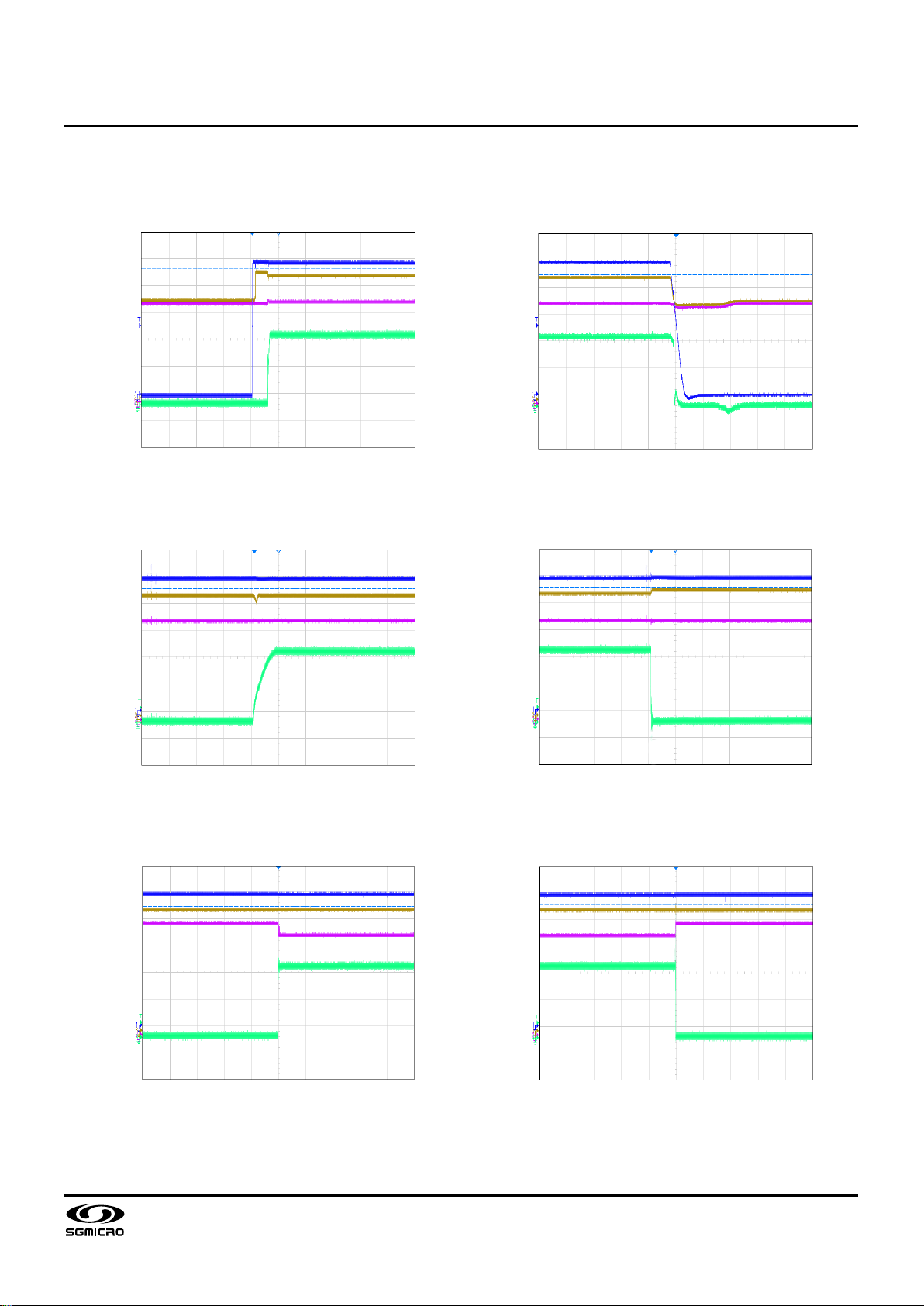
TYPICAL PERFORMANCE CHARACTERISTICS
TA= +25℃, VIN = 5V, IIN = 500mA, ICC = 128mA and VIN_MIN = 4.6V, unless otherwise noted.
Battery Charge Curve
Auto-Recharge
VIN
VSYS
VBAT
IBAT
1V/div 1V/div 1V/div 50mA/div
VIN
VSYS
VBAT
IBAT
1V/div 1V/d 1V/d 100mA/div
Time (4s/div)
Time (500ms/div)
CC Charge Steady State
SYS Load Transient
VIN
VSYS
VBAT
IBAT
1V/div 1V/div 1V/div 50mA/div
VIN
VSYS
ISYS
1V/div 1V/div 500mA/div
Time (2ms/div)
Time (500ms/div)
Input Current Limit-Based PPM
Input Voltage Regulation-Based PPM
VSYS
IBAT
IIN
ISYS
1V/div 100mA/div 100mA/div 200mA/div
VIN
VSYS
IBAT
ISYS
1V/div 1V/div 100mA/div 100mA/div
Time (4s/div)
Time (2s/div)
SGM41562A 500mA Single-Cell Li-Ion Battery Charger
SGM41562B with Power Path Management
8
JANUARY 2022
SG Micro Corp
www.sg-micro.com
TYPICAL PERFORMANCE CHARACTERISTICS (continued)
TA= +25℃, VIN = 5V, IIN = 500mA, ICC = 128mA and VIN_MIN = 4.6V, unless otherwise noted.
Power-On
Power-Off
VSYS
VBAT
VIN
IBAT
1V/div 1V/div 1Vdiv 50mA/div
VIN
VSYS
VBAT
IBAT
1V/div 1V/div 1Vdiv 50mA/div
Time (4ms/div)
Time (200μs/div)
Charge Enable
Charge Disable
VIN
VSYS
VBAT
IBAT
1V/div 1V/div 1Vdiv 50mA/div
VIN
VSYS
VBAT
IBAT
1V/div 1V/div 1Vdiv 50mA/div
Time (400μs/div)
Time (400μs/div)
BATT Insertion
BATT Removal
VIN
VSYS
VBAT
IBAT
1V/div 1V/div 1Vdiv 50mA/div
VIN
VSYS
VBAT
IBAT
1V/div 1V/div 1Vdiv 50mA/div
Time (500ms/div)
Time (500ms/div)

SGM41562A 500mA Single-Cell Li-Ion Battery Charger
SGM41562B with Power Path Management
9
JANUARY 2022
SG Micro Corp
www.sg-micro.com
TYPICAL PERFORMANCE CHARACTERISTICS (continued)
TA= +25℃, VIN = 5V, IIN = 500mA, ICC = 128mA and VIN_MIN = 4.6V, unless otherwise noted.
NTC Rising
NTC Falling
VSYS
VBAT
VNTC
IBAT
1V/div 1V/div 1Vdiv 100mA/div
VNTC
VSYS
VBAT
IBAT
1V/div 1V/div 1Vdiv 100mA/div
Time (10ms/div)
Time (10ms/div)
PCB_OTP at Charge Mode
PCB_OTP at Discharge Mode
VNTC
VSYS
VBAT
IBAT
1V/div 1V/div 1Vdiv 100mA/div
VNTC
VBAT
VSYS
IBAT
1V/div 1V/div 1Vdiv 1A/div
Time (2s/div)
Time (2s/div)
V
IN
OVP Operation
System Reset Function Operation Profile
VSYS
VIN
VBAT
IBAT
1V/div 1V/div 1Vdiv 100mA/div
VINT
VBAT
VSYS
5V/div 5V/div 5Vdiv
Time (2s/div)
Time (2s/div)
tRST_DGL = 8s, tRST_DUR = 2s
SGM41562A 500mA Single-Cell Li-Ion Battery Charger
SGM41562B with Power Path Management
10
JANUARY 2022
SG Micro Corp
www.sg-micro.com
TYPICAL PERFORMANCE CHARACTERISTICS (continued)
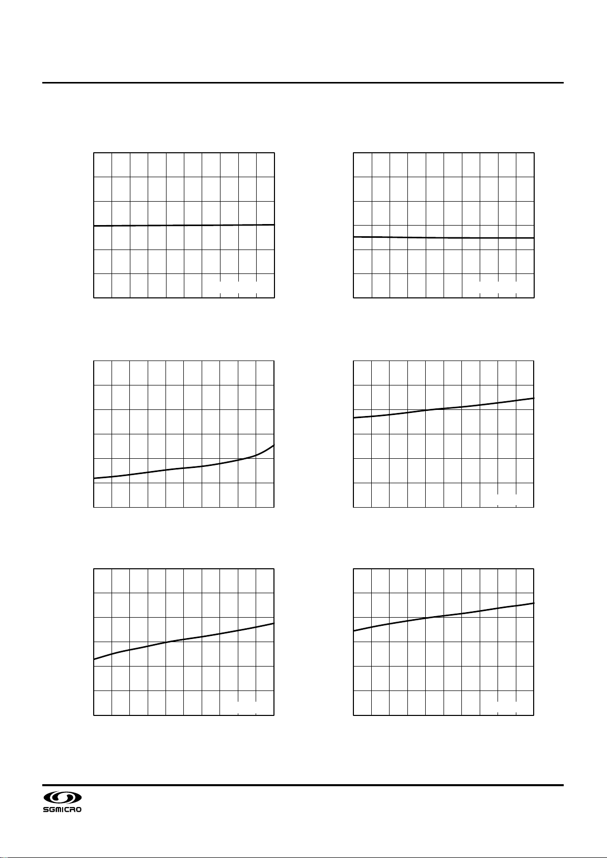
TA= +25℃, VIN = 5V, IIN = 500mA, ICC = 128mA and VIN_MIN = 4.6V, unless otherwise noted.
Battery Charge Regulation Voltage vs. Temperature
System Regulation Voltage vs. Temperature
Battery Current under Shipping Mode vs. Temperature
Pre-Charge Current vs. Temperature
Fast Charge Current vs. Temperature
Charge Termination Current vs. Temperature
3.9
4.0
4.1
4.2
4.3
4.4
4.5
-40 -25 -10 520 35 50 65 80 95 110
Battery Charge Regulation Voltage (V)
Temperature (℃)
VBAT_REG = 4.2V
4.4
4.5
4.6
4.7
4.8
4.9
5.0
-40 -25 -10 520 35 50 65 80 95 110
System Regulation Voltage (V)
Temperature (℃)
VSYS_REG = 4.65V
0.0
0.5
1.0
1.5
2.0
2.5
3.0
-40 -25 -10 520 35 50 65 80 95 110
IBAT_Q_SHIPPING (µA)
Temperature (℃)
1.0
1.5
2.0
2.5
3.0
3.5
4.0
-40 -25 -10 520 35 50 65 80 95 110
Pre-Charge Current (mA)
Temperature (℃)
IPRE = 3mA
100
110
120
130
140
150
160
-40 -25 -10 520 35 50 65 80 95 110
Fast Charge Current (mA)
Temperature (℃)
ICC = 128mA
1.0
1.5
2.0
2.5
3.0
3.5
4.0
-40 -25 -10 520 35 50 65 80 95 110
Charge Termination Current (mA)
Temperature (℃)
ITERM = 3mA

SGM41562A 500mA Single-Cell Li-Ion Battery Charger
SGM41562B with Power Path Management
11
JANUARY 2022
SG Micro Corp
www.sg-micro.com
TYPICAL PERFORMANCE CHARACTERISTICS (continued)
TA= +25℃, VIN = 5V, IIN = 500mA, ICC = 128mA and VIN_MIN = 4.6V, unless otherwise noted.
Battery OVP Voltage vs. Temperature
Input Current Limit vs. Temperature
Input Minimum Voltage vs. Temperature
Production Distribution
4.0
4.1
4.2
4.3
4.4
4.5
4.6
-40 -25 -10 520 35 50 65 80 95 110
Battery OVP Voltage (V)
Temperature (℃)
VBAT_REG = 4.2V
200
300
400
500
600
700
800
-40 -25 -10 520 35 50 65 80 95 110
Input Current Limit (mA)
Temperature (℃)
IIN_LIM = 500mA
4.50
4.55
4.60
4.65
4.70
4.75
4.80
-40 -25 -10 520 35 50 65 80 95 110
Input Minimum Voltage (V)
Temperature (℃)
VIN_MIN = 4.6V
0
4
8
12
16
20
345
355
365
375
385
395
405
415
425
435
445
455
465
475
485
495
Percentage of Drivers (%)
400mA Discharge Current (mA)
5000 Samples
1 Production Lot

SGM41562A 500mA Single-Cell Li-Ion Battery Charger
SGM41562B with Power Path Management
12
JANUARY 2022
SG Micro Corp
www.sg-micro.com
FUNCTIONAL BLOCK DIAGRAM
IN SYS
Body
Switch
nINT
Interrupt
Control
Loop Control
Register Charger
Control
SCL
SDA I
2
C
Interface
VDD
LDO Regulator
BAT
BAT
I
IN_ILIM_REF
V
IN_DPM
Thermistor
Monitor
NTC
I
CHRG_REF
V
TERM_REF
V
SYSREG
VSYS
GND
Qrvs
Qswitch
gm_
I
LIM
gm_
V
DPM
gm_
sys
gm_
I
CHRG
gm_
V
TERM
BAT-20mV gm_
fwd
VSYS
Qbypass
6V
V
VIN
V
VIN
3.65V
OVP
nUVLO
PRECOND V
BAT
V
PRECON_REF
SLEEP
V
BAT
+ 150mV
V
VIN
V
TERM
- V
RECHG
V
BAT
RECHG
EOC
I
BATTERY
I
TERM_REF
I
BATTERY
Figure 2. Functional Block Diagram

SGM41562A 500mA Single-Cell Li-Ion Battery Charger
SGM41562B with Power Path Management
13
JANUARY 2022
SG Micro Corp
www.sg-micro.com
DETAILED DESCRIPTION
Introduction
The SGM41562A/B is a single-cell battery charger with power
path management function for Li-Ion and Li-polymer batteries.
The charge features include pre-charge, fast charge including
constant-current mode (CCM) and constant-voltage mode
(CVM), end-of-charge termination, auto-recharge, and a
built-in safe charge timer. The safe charge timer is used to
prevent over-charging or other issues if the host runs out of
control.
A bypass switch between IN and SYS pins, and a battery
switch between SYS and BAT pins are integrated to provide
complete power path management (PPM). The switches have
low on-resistances to minimize loss and heat. System load is
primarily powered from the input when it is available, and the
remaining input power is used to charge the battery if needed.
When the input source is weak, the load is powered partially
from the battery. This mode in which the battery provides the
power deficit is called supplement mode. Battery will provide
the full load power if input is removed or if VIN is out of range.
For battery charging, the power to the battery is regulated by
the battery switch. To prevent faulty charge conditions, input
voltage, input current, system voltage, chip temperature and
external temperature (sensed by NTC) are continuously
monitored during charge.
Figure 3 shows the power paths and key internal blocks of the
device. The Qbypass switch regulates the voltage of the
system and the internal charge circuit. The Qrvs switch acts
as a near ideal blocking diode to prevent reverse power (or
leakage) from the load (SYS pin) back to the input (IN pin).
The Qswitch switch is responsible for battery charging
regulation and connecting or disconnecting of the battery
(BAT pin) to the system (SYS pin). The charge and discharge
circuits in the Figure 3 that are connected to the IN and BAT
pins have their own independent UVLO and power supply.
The rest of the chip is powered by either IN or SYS pin,
whichever has the higher voltage. The I/F interface (I2C
communication and nINT) block is active whenever any of the
power sources (IN or BAT pin) are available.
Qswitch
Qbypass
IN SYSQrvs
BAT
System LoadPower Input
UVLO
Charge
Circuit
UVLO
Discharge
Circuit
I/F
Interface
Figure 3. Power Path Management Structure
The chip has a watchdog timer as a protective feature against
unexpected host malfunctions. When watchdog timer is
enabled, it must be reset by host regularly to prevent
watchdog timer overflow that results in a chip reset and power
recycle. Watchdog reset is by writing into the watchdog
register through I2C interface (I/F). If the watchdog is not reset
on time, the power to the host will recycle.
The power fed to the SYS pin is recycled when watchdog
times out, the host does not response to IN power input
(when watchdog is forced on) or COLD_RESET bit is set to 1,
to clear the running environment before system program
upgrade or release from locked situations.
Input Detection
Figure 4 shows how the input voltage status is detected and
affects the device function along with the relevant timings and
nINT output signal updates. The device continuously monitors
the input voltage at the IN node. The SYS node and charge
circuit is only started and connected to the input when for a
duration of tINI, VIN is within its normal range (above VIN_UVLO
and below VIN_OVLO). Qbypass and Qrvs switches will turn off
as soon as an input UVLO or OVLO is detected.
As shown in Figure 4 any input state is considered stable if it
continuously stays in the same condition for a duration of tPWD
after which the device sends out a negative pulse to the nINT
pin with a pulse width of tINT_PULSE to inform the host about the
input state change.
The watchdog timer WATCHDOG[1:0] register is set to 01
once the valid input is detected and when an INT pulse is
asserted, which resumes its original setting when any writing
to this device occurs. If the host does not clear the watchdog,
power to the host is recycled for reset when watchdog runs
time out.
VIN_UVLO
VIN_OVLO
VIN
VIN_UVLO_HYS
VIN_OVLO_HYS
tPWD
tINI
tPWD tPWD
tINI
VSYS
tPWD
tINT_PULSE tINT_PULSE tINT_PULSE tINT_PULSE
nINT
IIN
Figure 4. Input Power Detection and nINT Signaling Timings
SGM41562A 500mA Single-Cell Li-Ion Battery Charger
SGM41562B with Power Path Management
14
JANUARY 2022
SG Micro Corp
www.sg-micro.com
DETAILED DESCRIPTION (continued)
Power Path Management
When the input voltage is normal and have enough headroom
for powering the system (VIN > VIN_UVLO and VIN - VSYS >
VHDRM), the input power path will conduct and the device
starts to power the system from input by setting the system
voltage to VSYS_REG. VSYS_REG is selected by programming
VSYS_REG[3:0] register, the lower 4 bits of REG07 (also
called system voltage register or VSYS_REG[3:0] register).
However, the actual system voltage (VSYS) can be affected by
the input voltage level, input current limit and battery voltage.
I2C commands can directly control the power paths. Input
path will be disconnected (high-impedance) by turning off
Qbypass switch if the EN_HIZ bit is set to 1. If the battery is
getting charge and Qswitch switch is on, it can also be
disconnected by setting charge enable bit, set the CEB bit to
1 (turn off Qswitch switch in charge direction). The power path
control bits are explained in Table 1. When these bits are
clear, they have no effect.
Table 1. Switch Control by I2C Interface
FETs EN_HIZ = 1 CEB = 1
Qbypass Off X
Qswitch (Charging) X Off
Qswitch (Discharging) X X
NOTE: X = Don't Care.
Battery Charge Profile
Figure 5 shows the battery charge profile used in this device.
The charge phases are explained below. Depending on the
I2C settings and the battery state of charge (SOC), some or
all of the phases may be skipped or used to finish a complete
charge cycle as explained below:
Pre-Charge: If the battery voltage is less than the pre-charge
threshold (VBAT_PRE), the battery is charged with the small
pre-charge current (IPRE). The pre-charge current value is the
same as the termination current (ITERM) that is programmed
via bit D[3:0] of the REG03, also called ITERM[3:0].
Constant-Current Charge: When battery voltage is higher
than VBAT_PRE, and less than VBAT_REG, it will be charged with a
constant current. The constant-current value is determined by
bit D[5:0] of the REG02 that is called ICC[5:0] and a single
scaling bit that if set, multiplies it by ¼. This bit is used for
finer CC adjustment (CC_FINE bit in REG0A).
Constant-Voltage Charge:When the battery voltage reaches
to the VBAT_REG, the voltage is kept constant and the charge
current drown by battery will start to fall. The VBAT_REG value is
determined by bit D[7:2] of the REG04 that is also called
VBAT_REG[5:0].
Charge Termination:A charge termination is recognized
when the charge current drops to a small value represented by
ITERM. If the termination detection is enabled by setting the
EN_TERM bit in REG05 D[4] to 1, then if the charge current
(ICHG) stays equal or lower than ITERM for a period of tTERM_DGL
(termination deglitching time) the charge cycle is considered
complete and charging current will be turned off and drop to
zero. With no termination, the charge current will continue to
drop. Note that a charge cycle is also considered complete and
charging will be turned off, if the safe timer function runs out of
time provided that the safe timer function is already enabled
by setting EN_TIMER bit in REG05 D[3] to 1.
Pre-Charge CC Charge CV Charge Termination Discharge Auto-Recharge
I
TERM
= I
PRE
I
PRE
V
BAT_PRE
V
BAT_REG
- V
RECH
V
BAT_REG
I
CC
Charge
Current
Battery
Voltage
Figure 5. Battery Charge Profile

SGM41562A 500mA Single-Cell Li-Ion Battery Charger
SGM41562B with Power Path Management
15
JANUARY 2022
SG Micro Corp
www.sg-micro.com
DETAILED DESCRIPTION (continued)
The charge status is updated to "charge complete" once the
termination condition is detected. The charge current will be
terminated when termination conditions are met and if the
TERM_TMR bit is set to 0 (REG05 D[0] = 0); the charge will not
terminate and current keeps decreasing if TERM_TMR bit is 1.
During the whole charging process, the actual charge current
may fall below the set values due to the other regulations or
controls such as dynamic power management (DPM)
regulation caused by insufficient input voltage or current or
due to thermal regulation. In thermal regulation the device
reduces the power path currents to keep junction temperature
below the programmed limit.
A new charge cycle starts when one of the following
conditions occurs:
The input power recycles (input on/off).
Battery charging is enabled by I2C command.
Auto-recharge kicks in due to battery charge state.
If all the following conditions are satisfied:
No NTC thermistor temperature fault.
No safety (charge) timer fault.
No battery over-voltage event.
The Qswitch switch is not forced to turn off (e.g. CEB = 1).
Battery Over-Voltage Protection
SGM41562A/B has a built-in battery over-voltage protection
limit. A battery over-voltage event is detected when battery
voltage is higher than VBAT_OVP + VBAT_REG. When this event
occurs, the charging is immediately suspended and a fault is
asserted. The discharging path will be turned on if battery
over-voltage condition does not clear and continues.
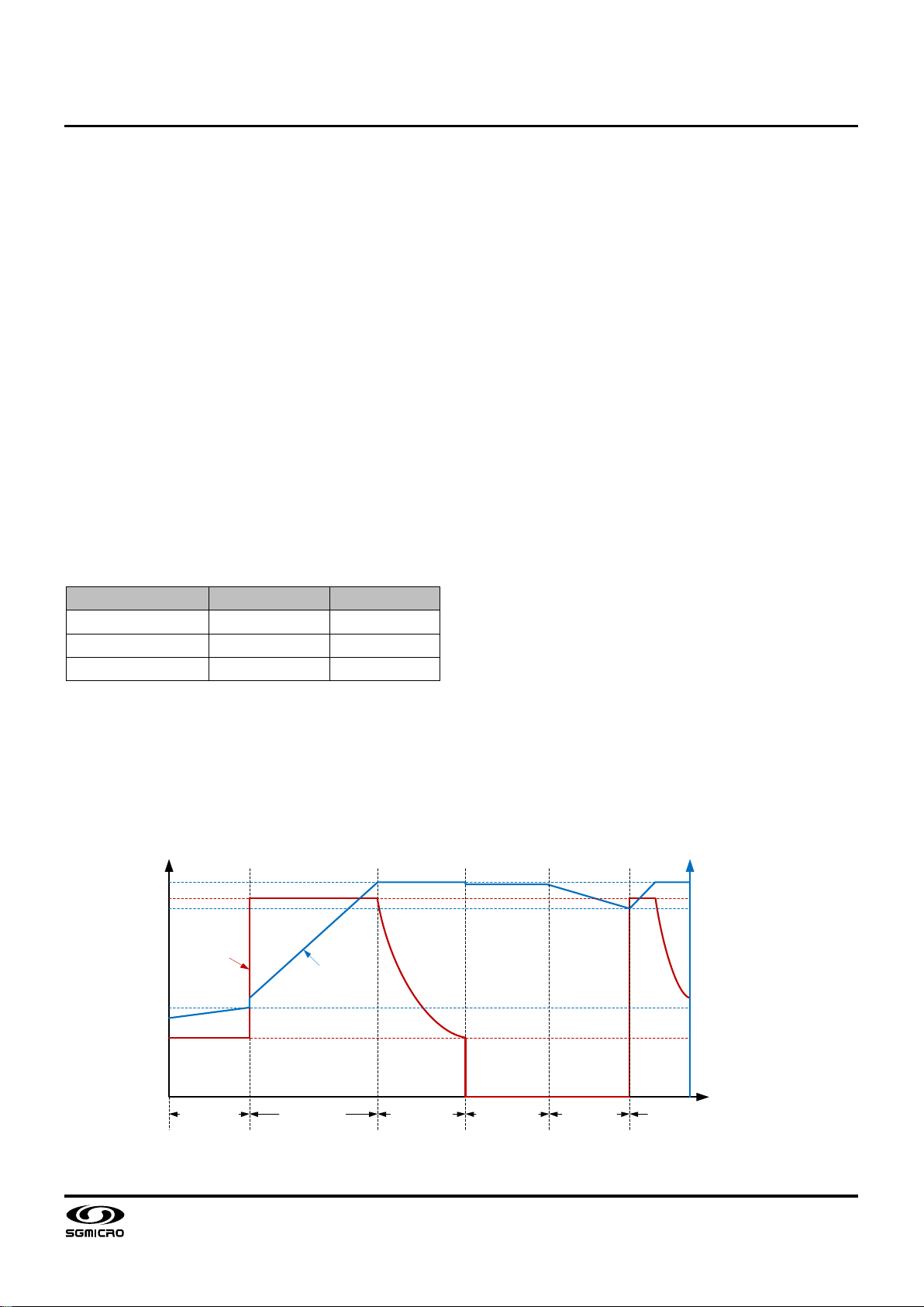
Input Current and Input Voltage Based
Power Management
Usually the input source (typically USB) is not strong enough
for all system power demands and a power management
scheme is needed to keep the system voltage in desired level
without over loading the source. Figure 6 shows the power
management profile and explains how it is implemented in
SGM41562A/B including the battery assist operation
(supplement) when input source is not able to provide
required power.
The input current is continuously monitored to make sure the
input source maximum current limit specification is met. The
total input current limit is programmable by I2C and is used to
prevent over loading of the input source.
If the input source is weak and the programmed input current
limit is higher than the effective capability of the source (like in
a dynamic loading condition) the back-up power management
will come in effect to prevent over loading of the input source.
The back-up power management is based on limiting the
input voltage drop to VIN_MIN value (programmable). The
voltage based dynamic power management (DPM) will
regulate the input voltage to VIN_MIN when the load is higher
than the input current capacity. If input current and voltage
limit are both reached, then the Qbypass switch (between IN
and SYS pins) will regulate and limit the total power taken
from the input. With the power limiting, if the system voltage
drops to the minimum value of (VSYS_REG - 90mV) or the input
voltage falls below (VIN - 160mV), the device will finally
reduce the charge current to prevent further voltage drops.
The programmed VIN_MIN must be at least 250mV higher than
VBAT_REG to assure stable operation of the regulator.

SGM41562A 500mA Single-Cell Li-Ion Battery Charger
SGM41562B with Power Path Management
16
JANUARY 2022
SG Micro Corp
www.sg-micro.com
DETAILED DESCRIPTION (continued)
I
SYS
I
IN
V
BAT
V
SYS
I
BAT
MIN(V
SYS_REG
- 90mV, V
IN
- 160mV)
30mV
10mV
I
DSCHG
× R
ON_BATFET
0
Charging
Discharging
Figure 6. Dynamic Power Management and Battery Supplement Operation Profile
Battery Supplement Mode
As mentioned above, the DPM will reduce the charge current
to keep the input current or voltage in regulation when source
power is not sufficient for system demand. If the charge
current is reduced to zero but still due to heavy system load
the input source is overloaded and VSYS continues to drop,
then the battery will supply the deficit to assist the input
source. This mode is called battery supplement mode in
which the battery provides IDSCHG as supplement current to
the load. This mode starts when the system drop reaches to
30mV below the battery voltage. In this mode the Qswitch
switch acts as a near ideal diode from battery to the system.
The Qswitch switch is controlled to regulate and maintain the
VBAT - VSYS drop to a fixed 10mV value when IDSCHG ×
RON_BATFET is less than 10mV. If IDSCHG × RON_BATFET is larger
than 10mV, the Qswitch switch is fully turned on to pass
battery voltage to the system with minimum drop.
In the battery supplement mode the ideal diode mode will be
disabled as soon as the system load decreases and VSYS
exceeds the VBAT + 20mV value.
When VIN source is not available, the device operates in
discharge mode (battery power) in which the Qswitch switch
is always fully on to reduce the losses.
Battery Regulation Voltage
The battery voltage for the constant-voltage regulation phase
(CV) is represented by VBAT_REG.
Thermal Regulation and Shutdown
SGM41562A/B continuously monitors its internal junction
temperature to avoid junction overheating while keeping the
power delivery at its maximum. When the internal junction
temperature reaches its programmable limit (TJ_REG), the
device starts to reduce the charge current to prevent higher
power dissipation. The thermal regulation limit is
programmable to help adjusting the design for the thermal
requirements in different applications. 4 different junction
temperature regulation thresholds (default 120℃) can be
chosen by programming the TJ_REG[1:0] register. In
particular, it is recommended that the junction temperature be
set not lower than the ambient temperature at which the
device charging behavior may occur.
The device fixed thermal shutdown limit (TJ_SHDN) is slightly
higher than the highest programmable TJ_REG. If TJrises
above this limit, both Qbypass and Qswitch switches will turn
off.

SGM41562A 500mA Single-Cell Li-Ion Battery Charger
SGM41562B with Power Path Management
17
JANUARY 2022
SG Micro Corp
www.sg-micro.com
DETAILED DESCRIPTION (continued)
NTC Function and VDD Gating
The NTC pin is provided to sense the battery temperature
using an NTC thermistor. Thermistors are usually included in
the rechargeable battery packs to ensure safe operation by
monitoring the battery temperature and making sure it is
between hot and cold limits. To adjust the temperature limits
for the device, two resistors (RT1 and RT2 in Figure 13) should
be connected to NTC pin as a divider between VDD and GND
pins. The thermistor itself is connected between NTC pin and
GND. The voltage on the NTC pin is determined by all three
resistors. This resistor divider along with the hot and cold limit
voltages defined in the EC table determines the hot-cold
operating window. Note that due to the negative temperature
coefficient of NTC, when its voltage drops below VHOT, it
means the battery temperature is exceeding the hot limit. The
NTC protection function can be disabled by clearing the
EN_NTC bit to 0. The default settings for NTC function are
the PCB OTP levels specified in EC table that can be change
by I2C as explained in Table 2.
Table 2. NTC Function Selection
I2C Control Function
EN_NTC EN_PCB OTP
0 don't care Disable
1 1 NTC
1 0 PCB OTP
NTC function only works in charge mode. When NTC pin
voltage falls out of the hot-cold window it means that the
temperature is outside the safe operating range and results in
a pause in charging and sets the fault bits. Charging will
resume when the temperature falls back into the safe range.
If DIS_VDD bit is disabled and VIN is removed, VDD power
turns off and becomes high-impedance leaving only RT2 in
parallel with the NTC thermistor. If DIS_VDD bit is enabled,
VDD remains active. VDD uses battery power if VIN is removed.
With PCB OTP selected, if the NTC pin voltage is lower than
the NTC hot threshold, Qbypass and Qswitch switches will
turn off. The PCB OTP fault also will set the NTC_FAULT
status bit to 1. The operation will resume when the NTC pin
voltage goes back above the NTC hot threshold.
Safety Timer
Using an internal safety timer, SGM41562A/B is capable to
limit the maximum duration of the pre-charge and charge
periods to avoid extended charging cycles that may happen
due to abnormal battery conditions. This protection can be
disabled by I2C. The safety timer starts counting if one of the
following occurs:
A new charge cycle is started.
Write in REG01 D[3] bit: from 1 to 0 (charge enable)
Write in REG05 D[3] bit: from 0 to 1 (safety timer enable)
Write in REG02 D[7] bit: from 0 to 1 (software reset)
Write in REG0A D[4] bit: from 0 to 1 (software power recycle)
The safety time limit is 1 hour for pre-charge condition in
which the battery voltage stays lower than VBAT_PRE and
cannot go higher. For the charge phase the time limit is
programmable through I2C and the safety timer starts
counting when the battery enters in constant-current charge
mode or constant-voltage charge mode.
Host Mode and Default Mode
SGM41562A/B can operate in either default mode (with default
parameters) or host mode (parameters programmed by host).
It will go to the default mode if one of the following occurs:
Input refresh with no battery connected.
Re-insert battery with no input source connected.
Device registers reset by writing 1 to REG_RST bit.
Watchdog timer expiry.
Upon a power-on reset, the device starts in default mode and
in the same state as if watchdog timer expiration has
occurred. In this mode all registers take their default values,
including EN_HIZ = 0 and CEB = 1, that means the input
power path is enabled and device is set to battery discharge
mode. Note that by default the battery will not be charged
after a reset.
When the device is in the host mode, watchdog function can
be activated and works in both charge and discharge modes
(Watchdog timer is independent of the charge safety timer).
Watchdog timer can be enabled by programming a non-zero
expiry time in its register, that is WATCHDOG[1:0] ≠00. If
watchdog timer is enabled, it must be reset regularly before it
runs out of time by writing 1 to WD_RST bit in REG02.
Otherwise the watchdog timer will expire and results in a
power recycle to the system. Therefore, resetting the
watchdog timer by host must happen in the intervals shorter
than watchdog time limit. The power recycle is performed by
turning off Qswitch and Qbypass for a duration of tRST_DUR and
then turning them on again. After watchdog timer expiration,
all registers will reset to their default values and the device
goes to the default mode.
To reduce the quiescent current during discharge mode, the
watchdog timer can be turned off by setting the
EN_WD_DISCHG bit to 0. If the WATCHDOG[1:0] is set to 00,
the watchdog timer is disabled under charge and discharge
modes independent of the EN_WD_DISCHG bit value.

SGM41562A 500mA Single-Cell Li-Ion Battery Charger
SGM41562B with Power Path Management
18
JANUARY 2022
SG Micro Corp
www.sg-micro.com
DETAILED DESCRIPTION (continued)
Battery Discharge Function
If the battery is connected (VBAT is above the VBAT_UVLO
threshold) and the input source is missing, the Qswitch turns
fully on. The low on resistance of the Qswitch minimizes the
conduction loss during discharge. The quiescent current of
the device is as low as 12μA in this mode. By setting REG0A
D[3] bit to 1, the Qswitch will stay on even if the rest of the
internal blocks are turned off, to reduce the device quiescent
current to less than 1.2μA. The low on-resistance and low
quiescent current of the device extend the run time.
Over-Discharge Current Protection
The over-discharge current protection is effective in discharge
mode and supplement mode. If the IBAT exceeds discharge
current limit value programmed in the REG03 D[7:4], the
Qswitch turns off after a wait delay (tDSCHG_CUT) and then
resumes conducting after a retry delay time (tRETRY).
When the battery voltage falls below the VBAT_UVLO limit that is
programmed in the REG01 D[2:0], the Qswitch turns off to
prevent over-discharging the battery.
If SWITCH_MODE bit (REG0A D[3]) is set to 1, the Qswitch is
forced to remain on like a simple switch and the over-
discharge is ignored during battery discharge. This bit will
reset if power is re-applied to the input. It will also reset if the
battery is connected or disconnected while power is applied
to the input.
System Short Circuit Protection
If a short circuit (to GND) occurs on the load connected to
SYS pin, the Qswitch disconnects the BAT to SYS path and
the Qbypass limits the current flowing in the IN to SYS path. If
the short circuit persists, the die temperature goes high and
causes a thermal shutdown.
Interrupt to Host (nINT Pin)
The nINT output signal is provided to alert the host on power
events. SGM41562A/B sends out a negative pulse (width =
tINT_PULSE) to nINT if any of the following events occurs:
A good input source is detected (UVLO < VIN < OVLO).
UVLO or OVLO is detected (input).
Charge completed.
A charging status change.
A fault record in REG09 occurs (input fault, thermal fault,
safety timer fault, battery OVP fault or NTC fault).
Watchdog expiration (WTD_FAULT in REG08 D[7]).
When one of the mentioned faults occurs, the relevant fault
bit will latch in the register except for NTC fault bit that always
reports the current status of the thermistor. A fault status bit is
unlatched if the device quits that fault state. It will reset to 0
after the host reads the register if the bit is unlatched.
The assertion of nINT signal pulse can be masked for some
of the events listed above when the corresponding mask
control bits are set in REG06 D[4:0]. If a mask bit is set, and
the event occurs, the nINT signals stays high.
The nINT pin is also used as an input to initiate a power
recycle on the SYS output for example when a turn off/turn on
is needed on the system when battery is not removable. This
input is also used to exit the shipping mode that keeps the
battery disconnected.

SGM41562A 500mA Single-Cell Li-Ion Battery Charger
SGM41562B with Power Path Management
19
JANUARY 2022
SG Micro Corp
www.sg-micro.com
DETAILED DESCRIPTION (continued)
Battery Disconnection Function
When the battery is not removable, it’s essential to disconnect
the battery from the system to allow system power recycling
or to put that in the shipping mode. It is performed by forcing
the Qswitch to remain off by setting FET_DIS bit to 1. Table 3
explains how the SGM41562A/B can be programmed in
shipping mode (or to do a power recycle on SYS) and how to
exit the shipping mode. To exit shipping mode either the input
power should be applied to IN port, or a low voltage (ground)
should be applied to nINT pin for a short time (for example by
holding a push bottom).
Table 3. Shipping Mode Control
Items
Enter Shipping Mode
Exit Shipping Mode
FET_DIS = 1
nINT Pin
H to L for 2s
VIN Plug-in
Qbypass don't care don't care On
Qswitch
(Charging)
Off On On (64ms Later)
Qswitch
(Discharging)
Off On On (64ms Later)
The FET_DIS bit is used for battery disconnection control. If
the bit is set to 1, the device enters the shipping mode after a
delay time, which can be programmed by EN_SHIP_DGL[1:0].
After the delay the Qswitch turns off and the FET_DIS bit
resets to 0. The device wakes up from shipping mode by
pulling down nINT pin or detecting an acceptable voltage on
the IN pin. The device exits from shipping mode 2 seconds
after pulling nINT pin down or 64ms after detecting an
acceptable VIN. For the application of nINT pulled down to a
low voltage in the shipping mode, EN_SHIP_DGL[1:0] must
keep default value.
System power can be recycled by turning off the Qswitch and
Qbypass if nINT pin is pulled low for a duration of more than
tRST_DGL. It is the time delay to avoid noise and glitches or to
hold a push bottom. The tRST_DGL time is programmed by
tRST_DGL[1:0] in REG01. The off state lasts for a duration of
tRST_DUR which can be programmed via tRST_DUR in REG01.
After this time the Qswitch and/or Qbypass will be
automatically turned on and the system is powered again.
During the off period, the nINT pin is biased to a lower
voltage.
The waveforms of power recycling are shown in Figure 7.
VINT
VBAT
VSYS
5V/div 5V/div 5Vdiv
Time (2s/div)
Figure 7. Power Recycling Waveforms

SGM41562A 500mA Single-Cell Li-Ion Battery Charger
SGM41562B with Power Path Management
20
JANUARY 2022
SG Micro Corp
www.sg-micro.com
REGISTER MAPS
All registers are 8-bit and individual bits are named from D[0] (LSB) to D[7] (MSB).
I2C Slave Address: 03H
R/W: Read/Write bit(s).
R: Read only bit(s).
PORV: Power-On Reset value.
n: Parameter code formed by the bits as an unsigned binary number.
REG00
Register address: 0x00; R/W
PORV = 10011111
Table 4. REG00 Register Details
BITS BIT NAME DESCRIPTION COMMENT PORV TYPE RESET BY
D[7:4] VIN_MIN[3:0]
VIN_MIN[3]
1 = 640mV
Minimum Input Voltage Limit (n: 4 bits):
= 3.88 + 0.08n (V)
Offset: 3.88V
Range:3.88V (0000) - 5.08V (1111)
Default: 4.60V (1001)
1 R/W REG_RST
VIN_MIN[2]
1 = 320mV
0 R/W REG_RST
VIN_MIN[1]
1 = 160mV
0 R/W REG_RST
VIN_MIN[0]
1= 80mV
1 R/W REG_RST
D[3:0] IIN_LIM[3:0]
IIN_LIM[3]
1 = 240mA
Input Current Limit (n: 4 bits):
= 50 + 30n (mA)
Offset: 50mA
Range: 50mA (0000) - 500mA (1111)
Default: 500mA (1111)
1 R/W REG_RST
IIN_LIM[2]
1 = 120mA
1 R/W REG_RST
IIN_LIM[1]
1= 60mA
1 R/W REG_RST
IIN_LIM[0]
1 = 30mA
1 R/W REG_RST
REG01
Register address: 0x01; R/W
PORV = 10101100
Table 5. REG01 Register Details
BITS BIT NAME DESCRIPTION COMMENT PORV TYPE RESET BY
D[7:6] tRST_DGL[1:0]
00 = 8s
01 = 12s
10 = 16s (default)
11 = 20s
nINT Pull-Down Period to Disconnect the
Battery (n: 2 bits):
= 8s + 4n (seconds)
1 R/W
REG_RST
or Watchdog
0 R/W
REG_RST
or Watchdog
D[5] tRST_DUR 0 = 2s
1 = 4s (default)
Battery FET off-time duration after reset.
The Qbypass and Qswitch off-time before auto
turn-on.
1 R/W REG_RST
or Watchdog
D[4] EN_HIZ
HIZ Mode Enable
0 = Disable (default)
1 = Enable
Control Qbypass switch.
Default: disable (0) or switch on
Note: The EN_HIZ bit only controls the on and
off of the Qbypass.
0 R/W REG_RST
or Watchdog
D[3] CEB
Setting Charge Enable
0 = Charge enable
1 = Charge disabled (default)
Charge enable/disable Qswitch configuration.
Default: charge disabled (1) or Qswitch off 1 R/W REG_RST
or Watchdog
D[2:0] VBAT_UVLO[2:0]
VBAT_UVLO[2]
1 = 360mV
Battery UVLO Threshold Value (n: 3 bits):
= 2.4V + 0.09n (V)
Offset: 2.4V
Range: 2.4V (000) - 3.03V (111)
Default: 2.76V (100)
1 R/W
REG_RST
or Watchdog
VBAT_UVLO[1]
1 = 180mV
0 R/W
REG_RST
or Watchdog
VBAT_UVLO[0]
1 = 90mV
0 R/W
REG_RST
or Watchdog
This manual suits for next models
1
Table of contents
Popular Batteries Charger manuals by other brands

Mastervolt
Mastervolt POWERCHARGER 12/40-3 quick start guide

Hama
Hama 87013 operating instructions

Metabo HPT
Metabo HPT UC 36YSL Safety instructions and instruction manual

Motomaster
Motomaster ELIMINATOR WORKSHOP 011-1980-4 instruction manual

LEITZ
LEITZ Desktop Multicharger XL operating instructions

Craftsman
Craftsman 911 041 Operator's manual


