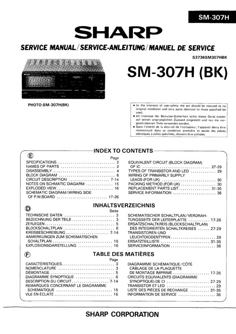
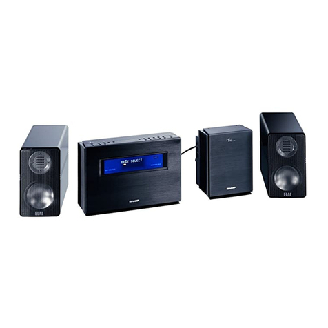
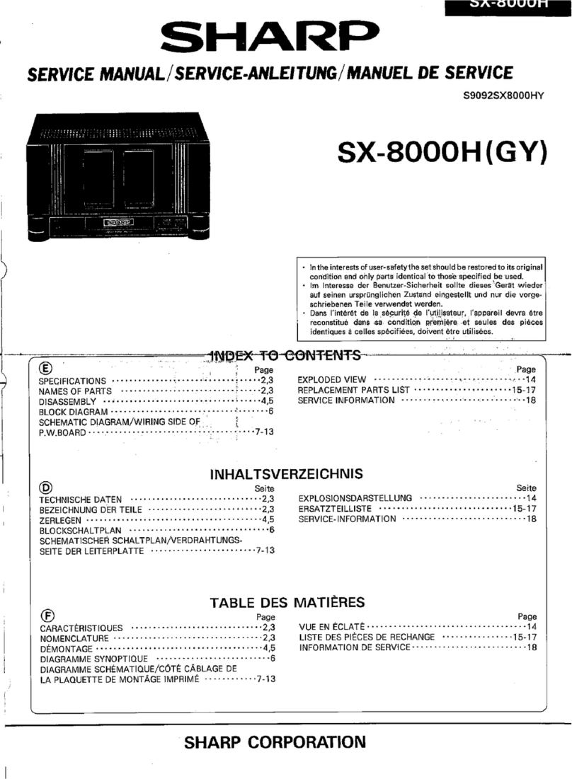
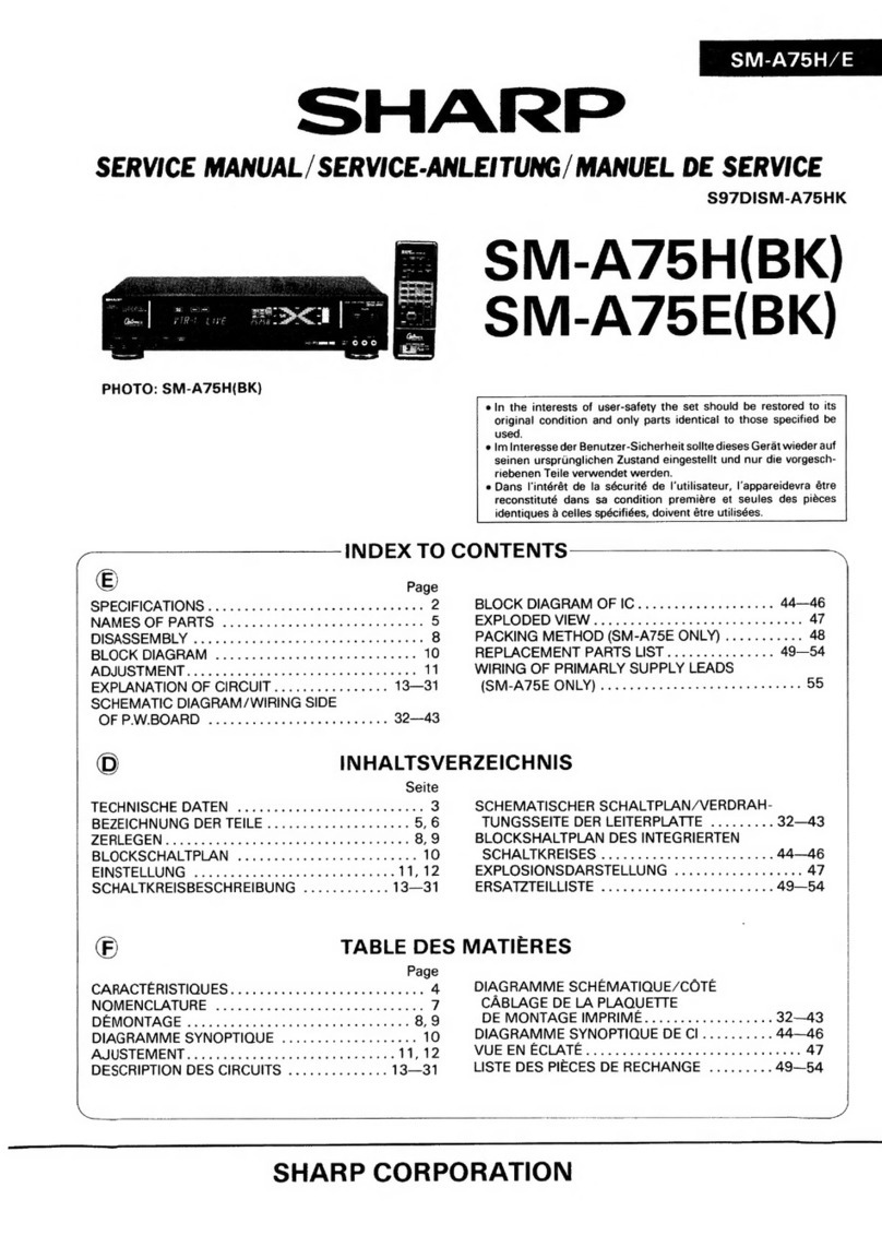
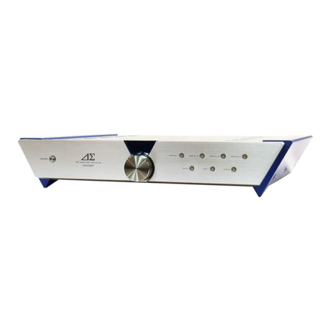
Sharp SM-SX1 User manual

SM-SX1/SX1W
– 1 –
SM-SX1
• In the interests of user-safety the set should be restored to its
original condition and only parts identical to those specified be
used.
SERVICEMANUAL
SHARP CORPORATION
No. S7063SMSX1///
This document has been published to be used
for after sales service only.
The contents are subject to change without notice.
CONTENTS
Page
IMPORTANT SERVICE NOTES (SM-SX1 FOR U.S.A. ONLY) .........................................................................................2
AC POWER SUPPLY CORD (SM-SX1W ONLY)...............................................................................................................2
SPECIFICATIONS ............................................................................................................................................................. 3
NAMES OF PARTS ........................................................................................................................................................... 3
OPERATION MANUAL .......................................................................................................................................................5
DISASSEMBLY.................................................................................................................................................................. 6
ADJUSTMENT ................................................................................................................................................................... 8
WIRING PROCESS DIAGRAM ....................................................................................................................................... 10
BLOCK DIAGRAM ........................................................................................................................................................... 12
SCHEMATIC DIAGRAM / WIRING SIDE OF P.W.BOARD..............................................................................................14
NOTES ON SCHEMATIC DIAGRAM .............................................................................................................................. 32
TYPES OF TRANSISTOR AND DIODE .......................................................................................................................... 32
WAVEFORMS OF CD CIRCUIT...................................................................................................................................... 33
TROUBLESHOOTING ..................................................................................................................................................... 34
FUNCTION TABLE OF IC................................................................................................................................................ 37
PARTS GUIDE/EXPLODED VIEW/PACKING OF PARTS (SM-SX1 FOR U.S.A. ONLY)
SACD DIGITAL1 DIGITAL2 LINE1 LINE2
MODEL
1-BIT AMPLIFIER
SM-SX1W
MODEL
1-BIT AMPLIFIER
All manuals and user guides at all-guides.com
all-guides.com

SM-SX1/SX1W
– 2 –
FOR A COMPLETE DESCRIPTION OF THE OPERATION OF THIS UNIT, PLEASE REFER
TO THE OPERATION MANUAL.
IMPORTANT SERVICE NOTES (FOR U.S.A. ONLY)
BEFORE RETURNING THE AUDIO PRODUCT
(Fire & Shock Hazard)
Before returning the audio product to the user, perform the
following safety checks.
1. Inspect all lead dress to make certain that leads are not
pinchedorthathardwareisnotlodgedbetweenthechassis
and other metal parts in the audio product.
2. Inspect all protective devices such as insulating materials,
cabinet,terminalboard,adjustmentandcompartmentcovers
or shields, mechanical insulators etc.
3. To be sure that no shock hazard exists, check for leakage
current in the following manner.
* Plug the AC line cord directly into a 120 volt AC outlet.
* Using two clip leads, connect a 1.5k ohm, 10 watt resistor
paralleled by a 0.15µF capacitor in series with all exposed
metal cabinet parts and a known earth ground, such as
conduit or electrical ground connected to earth ground.
* Use a VTVM or VOM with 1000 ohm per volt, or higher,
sensitivity to measure the AC voltage drop across the
resistor (See diagram).
* Connect the resistor connection to all exposed metal parts
havingareturnpathtothechassis(antenna,metalcabinet,
screw heads, knobs and control shafts, escutcheon, etc.)
and measure the AC voltage drop across the resistor.
AllcheckmustberepeatedwiththeAClinecordplugconnection
reversed.
Anyreadingof0.3voltRMS(thiscorrespondsto0.2milliamp.
AC.) or more is excessive and indicates a potential shock
hazard which must be corrected before returning the audio
product to the owner.
TO EXPOSED
METAL PARTS
CONNECT TO
KNOWN EARTH
GROUND
TEST PROBE
0.15 µF
1.5k ohms
10W
VTVM
AC SCALE
QACCB0114AFZZ
QACCZ0110AFZZ
QACCE0106AFZZ
QACCL0111AFZZ
AC POWER SUPPLY CORD (SM-SX1W ONLY)
All manuals and user guides at all-guides.com

SM-SX1/SX1W
– 3 –
Rated output power:
RMS; 50 W + 50 W (DIN 45 500)
Total harmonic distortion:
0.05 % (1 kHz, 1 W)
Frequency response:
10 Hz - 20 kHz (+1 dB, -1 dB)
10 Hz - 100 kHz (+1 dB, -3 dB)
Dynamic range:
100 dB (10 Hz - 20 kHz)
A/D noise shaping:
7th-order (delta-sigma) modulation
Input terminals:
DIGITAL1; RCA coaxial
DIGITAL2; Square type optical
SACD; RCA analog, 1 BIT digital
LINE 1,2; RCA analog (350 mV rms/50 k ohms)
Output terminals:
DIGITAL OUT; Square type optical
LINE OUT; RCA analog
Speakers; 8 ohms
Dimensions:
Width; 300 mm (11-13/16")
Weight:
Approx. 6.8 Kg (15.0 lbs.)
Height; 66 mm (2-5/8")
Depth; 411 mm (16-3/16")
120 V, 60 Hz
220-240 V, 50/60 Hz
230 V, 50 Hz
220 V, 50 Hz
110 - 120 V, 50/60 Hz
220- 240 V, 50/60 Hz
Power source:
North America
Australia,
New Zealand
Singapore
Hong Kong
Other countries
51 W
55 W
55 W
55 W
55 W
55 W
POWER
CONSUMPTION
POWER SOURCE
Specifications for this model are subject to change without
prior notice.
SPECIFICATIONS
NAMES OF PARTS
SACD DIGITAL1 DIGITAL2 LINE1 LINE2
3
24
1
4 Volume Control Knob
Controls the sound level.
To cut the output to the speaker with the
power turned on:
Set the sound level at “0” then press and
hold the corresponding input selector but-
ton for 2 seconds or more.
The signal output to the speaker returns
when you reset the sound level at “1” or
higher.
1 Power Button
Turns the unit on or off.
2 Input Selector Buttons
Used to select the equipment source you
want to play back.
When the power is turned on, the unit is
switched to “SACD”.
3 Volume Display
Displays the sound level within the range of
“0” - “128”.
All manuals and user guides at all-guides.com

SM-SX1/SX1W
– 4 –
7 Digital Output Terminal (OPTICAL)
Connect equipment using a square type
optical digital cable.
(OPTICAL)
78 9
LINE 1 LINE 2
SACD
LINE OUT
(COAXIAL)
DIGITAL 1 DIGITAL 2
DIGITAL OUT
(OPTICAL) (OPTICAL) RIGHT
+
-
RATED IMPEDANCE : 8
SPEAKERS
LEFT
+
-
65
5 Digital 1 Input Terminal (COAXIAL) *
Connect equipment using RCA coaxial
cable.
6 Digital 2 Input Terminal (OPTICAL) *
Connect equipment using the square type
optical digital cable.
This terminal send signals of the external
equipment connected to the DIGITAL 1 or 2
terminal.
*For digital input to this product, use
equipment which adapts to the digital
audio interface.
(32kHz, 44.1kHz, 48kHz)
8 Speaker Output Terminals
Plug the speaker cord in firmly and be care-
ful that the end of the cord does not touch
the next terminal or speaker cord, as this
could cause damage to the amplifier.
Use a speaker system which has 50 W or
more rated power input and 8 ohms im-
pedance.
If the volume is turned up too high with the
speakers of less than 8 ohms impedance con-
nected, the protection circuit of the amplifier
activates. Nothing is heard temporarily.
9 AC Input Jack
Connect the power cord to the AC INPUT
jack.
Speaker cord
2 Line 1 Input Terminals
Connect equipment using RCA cords.
3 Line 2 Input Terminals
Connect equipment using RCA cords.
1 Line Output Terminals
Connect equipment using RCA cords. 4 SACD/1-bit Signal Input Terminals
Connect the super audio CD player using
RCA cords or the 1-bit signal cable included
with your Sharp SACD player.
When both the RCA cords and the 1-bit
signal cable are connected, signals from
the latter have priority.
When nothing is connected to the 1 BIT in-
put terminal, signals from the RCA cords are
used.
(If you use the 1 BIT input terminal, refer to
the operation manual for the super audio CD
player.)
These terminals send signals of the external
equipment connected to the RCA (of the
SACD), LINE 1 or LINE 2 terminal.
12 4
3
LINE 1 LINE 2
SACD
LINE OUT
(COAXIAL)
DIGITAL 1 DIGITAL 2
DIGITAL OUT
(OPTICAL) (OPTICAL) RIGHT
+
-
LEFT +
-
RATED IMPEDANCE : 8
SPEAKERS
2
All manuals and user guides at all-guides.com

SM-SX1/SX1W
– 5 –
OPERATION MANUAL
Speakers
7th-order
(delta-sigma)
modulator
1-bit coding LSI
Fixed-voltage
high-speed
switching circuit Low-pass
filter network
1-bit
control
signals
Power
amplifier
switching
signal Out-
put
Fixed voltage
Analog signal
Multi-bit
digital signal
(32kHz, 44.1kHz, 48kHz)
1-bit signal
Over-
sampling
Direct input
(delta-sigma) dynamic feedback
This product uses 1-bit signals as control signals.As a result, amplification which maintains a
1-bit signal performance is realized by switching the fixed-voltage power with precise quartz-
crystal accuracy.
Adopting the concept of “ (delta-sigma) Dynamic Feedback”, this product enables stable am-
plification faithful to the original sound by sending back the power voltage fluctuations (which
affects the audio signal) to the “7th-order (delta-sigma) modulator 1-bit coding LSI” which
corrects the 1-bit control signal in real time.
Sampling the input signal at a high-frequency approx. 2.8 MHz (64 fs), the (delta-sigma)
modulation circuit yields a 1-bit signal stream which faithfully reproduces the original sound.
In this 7th-order (delta-sigma) modulation block, the quantization noise is shifted to a
higher band to generate 1-bit signals which secure high signal to noise ratio in the playback
band.
Using these 1-bit signals as control signals, the fixed-voltage high-speed switching circuit is con-
trolled. The signals abstracted from the switching circuit are sent to the low-pass filter network and
used to drive speakers.
This amplifier has no analog amplifier elements and can obtain speaker driving power by “creating
1-bit control signals through high-speed sampling” and “synchronized high-speed switching to the
sampling frequency”. In consequence, amplification with excellent movement and transient char-
acteristics is fulfilled.
1-bit amplification process
NOTES FOR USE
Notes:
Plug theAC power cord into a convenientAC
outlet, after any connections.
Unplug theAC power cord from theAC outlet
if the unit will not be in use for a prolonged
period of time.
Never use a power cord other than the one
supplied. Use of a power cord other than the
one supplied may cause an electric shock or
fire.
Speaker cord connection
Be sure that the power is turned OFF when
connecting the speaker cord. Failure to turn
the power off can result in a short circuit that
will place the amplifier into the protection cir-
cuit mode and cause the amplifier to shut
down. If this occurs, make sure that the am-
plifier is off, then disconnect the power cord
fromthe outlet to reset thecircuit breaker.You
can then reconnect the cord to use the am-
plifier.
Volume setting
Make sure to set the volume to the minimum
sound level before turning on the amplifier
poweror performing any inputswitching. Fail-
ure to do this may result in damage to your
speaker system.
The supply voltage of the switching circuit is
not linked with volume adjustment.
Therefore,aconstantvoltage is supplied even
if not playing back sound and residual sound
may be generated slightly such as when the
volume is turned up. This is normal.
If a problem occurs
If this product is subjected to strong external
interference(excessive shock, staticelectric-
ity, abnormal supply voltage due to lightning,
etc.) or if it is operated incorrectly, it may mal-
function.
In such a case, turn the power off.
Turn the power on again and check that the
product works normally.
(If problems still occur, contact the dealer.)
Before installation
Protectors are applied to all five feet.
Remove them before installation.
It is recommended to attach the three supplied
pads as shown below. This unit is supported at
three points.
Thepadsprevent slippage or damaging therack.
Protector
Middle foot at the back
Connecting the AC power cord
To AC INPUT
To an AC outlet
Pad
Power supply voltage:
Thevoltage used by thisproduct varies, depend-
ingon the shippingdestination. Check if the volt-
age written on the left side panel of the unit is
suitable for that of your country.
All manuals and user guides at all-guides.com

SM-SX1/SX1W
– 6 –
DISASSEMBLY
Caution on Disassembly
Follow the below-mentioned notes when disassembling
the unit and reassembling it, to keep it safe and ensure
excellent performance:
1. Be sure to remove the power supply plug from the wall
outlet before starting to disassemble the unit.
2.Take offnylonbands orwire holders wherethey needto
beremovedwhendisassemblingtheunit.Afterservicing
theunit, besure to rearrangethe leadswhere they were
before disassembling.
3. Take sufficient care on static electricity of integrated
circuits and other circuits when servicing.
Figure 6-2
Figure 6-1
Figure 6-3
1 Top Panel 1. Hexagon Screw......(A1) x5 6-1
2 Side Panel 1. Hexagon Screw......(B1) x6 6-2
(Left/Right)
3 Front Panel 1. Screw .................... (C1) x4 6-2
2. Socket ................... (C2) x1
4 Rear Panel 1. Screw .................. (D1) x16 6-2
2. Socket ................... (D2) x2
5 Side Bracket 1. Screw ...................(E1) x14 6-3
(Left/Right) 2. Socket ....................(E2) x3
6 Front Bracket 1. Screw ..................... (F1) x1 7-1
2. Nut ..........................(F2) x1
3. Screw ..................... (F3) x8
4. Socket .................... (F4) x1
7 Shield Cover A 1. Screw .................... (G1) x4 7-2
8 Shield Cover B 1. Screw .................... (H1) x4 7-2
9 Microcomputer 1. Socket .................... (J1) x2 7-3
PWB 2. PWB Holder ........... (J2) x4
10 Main PWB 1. Screw .....................(K1) x5 7-3
2. Socket ....................(K2) x5
11 Power PWB 1. Screw ..................... (L1) x8 7-4
2. Screw ..................... (L2) x2
3. Socket .................... (L3) x2
12 AC Input Filter 1. Screw .................... (M1) x1 7-4
PWB 2. PWB Holder .......... (M2) x3
13
Input Source PWB
1. Screw .................... (N1) x1 7-4
14 1 Bit Amp. PWB 1. PWB Holder ...........(P1) x4 7-4
15 Selector Switch 1. Screw .................... (Q1) x5 7-5
PWB 2. Socket ................... (Q2) x1
3. Claw ...................... (Q3) x2
16
Segment PWB 1.
Screw......................(R1) x4 7-5
2. Claw ...................... (R2) x4
REMOVAL PROCEDURE
STEP FIGURE
(A1)x5
ø4x6mm
(B1)x3
ø3x8mm
(B1)x3
ø3x8mm
Top Panel
Front Panel
Side Panel
Right(Right)
Side Panel
(Left)
Rear Panel
(D1)x13
ø3x6mm
(D1)x2
ø3x6mm
(D1)x1
ø3 x6mm
(C1)x2
ø3x8mm
(C1)x2
ø3x8mm
(C2)x1 (D2)x1
Front
Panel
Rear Panel
Shield
Plate
Power Filter
PWB
(D2)x1
Speaker
Relay PWB
Microcomputer
PWB
(E1)x5
ø3x6mm
(E1)x2
ø3x6mm
(E1)x2
ø3x6mm
(E1)x5
ø3x6mm
Side Bracket
(Left)
Side Bracket
(Right)
(E2)x3
Input Source
PWB
Microcomputer
PWB
All manuals and user guides at all-guides.com
all-guides.com

SM-SX1/SX1W
– 7 –
(G1)x4
ø3x6mm
(H1)x4
ø3x6mm
Shield
Cover A
Shield
Cover B
Main PWB
Front Panel
Selector
Switch PWB
Segment PWB
Washer
(Q1)x5
ø2x25mm
(R1)x4
ø2x12mm
(Q2)x1 (Q3)x2
(R2)x4
Selector
Switch PWB
Segment
PWB
Pull
Pull
Pull
(J2)x4
(J1)x2
(K1)x5
ø3 x6mm
(K2)x3
(K2)x2 Microcomputer
PWB
Main PWB
Push
Push
Microcomputer
PWB
Pull
1
2
Figure 7-3
Figure 7-5
Figure 7-2
Figure 7-1
Figure 7-4
(F3)x4
ø3x6mm
(F3)x2
ø3x6mm
(F4)x1
(F3)x2
ø3x6mm
Front
Bracket
Power PWB
Volume
Bracket
Volume
Knob
Washer
Washer
Power Knob
(F1)x1
ø3x8mm
(F2)x1
AC Input
Filter PWB
UNT501, 502
Input Source
PWB
1 Bit Amp PWB
(L1)x8
ø3x8mm
(L2)x2
ø3x6mm
(M1)x1
ø3x6mm
(N1)x1
ø3 x6mm
(L3)x2 (M2)x3
(P1)x4
AC Input
Filter PWB
1
2
1 Bit Amp
PWB
1
2
Push
Pull
Push
Pull
All manuals and user guides at all-guides.com

SM-SX1/SX1W
– 8 –
ADJUSTMENT
Measurethenoisedistributionbetweenthesetoutputterminals(Lch+,Lch-andRch+, Rch-), and adjust VRA1 to VRA4. The VRA
adjustment sequence is the same as that of the offset voltage adjustment.
Measuring instrument: Yokokawa Electric brand SA2400
Measurement range : Refer to Fig. 8-2.
Adjustable range:
1
250Hz to 100kHz within ±3dB from the standard noise curve
2
(Noise strength of 125Hz) — (Noise strength of 250Hz) 20dB
AC POWER
SUPPLY
UNIT Specterum
Analyzer
Speaker terminal
Apply the analyzer between Lch+ and Lch-,
and between Rch+ and Rch-.
Figure 8-1
Standard noise floor curve
(Frequency range 1)
Figure 8-2
20dBV
Following
All manuals and user guides at all-guides.com

SM-SX1/SX1W
– 9 –
Output
Connector
-22V Side
-22V Side
+22V Side
+22V Side
semifixed VOL
semifixed VOL
G
AFrom Main PWB
Output
Connector
1-bit PWB adjusting method
Connect as shown Fig. 9-2.
AC IN 110-120, 220-240, 230V
AC POWER SUPPLY
UNIT Digital Multimeter
Figure 9-2
AC/DC switching power supply, Output voltage adjustment
Figure 9-1
Check that the AC/DC output voltage is ±22V ±0.15V at the
A
connector.(Ifdifferent,adjustthevoltageusingthesemifixed
VOL as described above.)
[Simplified offset voltage adjustment]
1. It is fitted to the mechanical center of VRA1, VRA2, VRA3, and VRA4.(FIg. 10-1)
2. Connect the digital multimeter to the terminals of the speaker, and adjust the voltage between + and – of each terminal to 0 ±
10 mVolt with VRA1 (L-ch) or VRA2 (R-ch). (Fig.9-3)
DIGITAL OUT
(OPTICAL) RIGHT
+
-
RATED IMPEDANCE : 8
SPEAKERS
LEFT
+
-
R-ch 8Ω SP Terminal L-ch
Figure 9-3
All manuals and user guides at all-guides.com

SM-SX1/SX1W
– 10 –
(1 BIT PWB)
Figure 10-1
WIRING PROCESS DIAGRAM
Figure 10-2
Approx.60mm
B1
side
B1
side
Windonce.
Connector
side
Connector
side
Tiewithnylonband.
Windtheleadwirearoundthecore
once.Mountthecoreandlockit.
Then,tiethemtogethernylonband.
Nylonband
Coremountingposition
Windthe5Pleadwire,as
shown,oncearoundeach
core . Mountthecoresand
lockthem.Then,insertthe
connectors.
Placethecorearoundthe
positionshownabove.
Afterprocessingthecore,insertthe12Pconnectorfrom
theterminalPWB.
(MicrocomputerPWBCNP904)(SeeFig.-A.)
F i g -B
30mm
30mm
5P
Pull out the lead wires from above.
Press the lead wires wound around
the core toward the SP relay PWB.
Press the core to the terminal
board with the core stood.
core
core
F i g - A
Placethecorenearthe
connector.
Twistthe12Pleadwireandwindit
aroundcoreonce(neartheconnector).
Mountthecoreandlockit.Then,insert
theconnectors.
Fixthecoretotheaperture
usingnylonband.
(Headinside)
Afterfixingthecore, insertthe5Pconnectorfrom
thedigitalPWB.(SeeFig.-B.)
Insert the 2P connector
from the inlet.
Detail drawing of winding lead wire
around the core
core
Push in the core.
Push in the core.
All manuals and user guides at all-guides.com

SM-SX1/SX1W
– 11 –
Push the core of the SP lead wires into the
space between the shield case and the
speaker relay PWB. (The direction of the
core can be either vertical or horizontal.) Mount the core to the 11P lead wire.
Avoid.
70 5
5P
4PB 1
5P
4P
6P
4P
3P
3P
2P
2P
After passing through the cores, insert the
terminals in the 4P and 6P housings.
Core
Afterwindingtheleadwirearoundthecore,
insertthe7PconnectorfromtheSPrelay
PWBintheterminalPWB.(Performthe
abovebyplacingthecorearoundtheplace
shown).Becarefulnottotouchthescrew.
To avoid unnecessary radiation, attach felt to
each lead wire and fix it to the case in order
that the lead wires do not overlap each other
(to prevent the contact of each lead wire).
Figure 11
All manuals and user guides at all-guides.com
all-guides.com

SM-SX1/SX1W
– 12 –
DIGITAL SIGNAL
ANALOG SIGNAL
RELAY CONTROL
PROTECT
3
13
13
3
7
8
10
1
6
4440
37
~
~
31
~
5
1
3
~
38
39
42
35 27 33
1
13
3
8
5
11
11
1
9 5
10
12
1
12
11
15
17
~
18
20
24
25
26
38
123
29 26 33 35 41 43
~
~~
1
3
~
11
17
~
5
13
J101
LINE2
LINE
OUT
RLY101
Q101
RLY102
Q102
RLY103
Q103
DIGITAL/ANALOG
CHANGE
RLY802
Q803
VOL301
MAIN
VOLUME
DIGITAL/ANALOG
CHANGE
RLY301,
RLY302
Q301
Q302
A
Q
I
C
AB
IC102
INVERTER
74HC153F
IC103
BUFFER
AMP.
74HCT04F
1BIT TERMINAL
RX101
DIGITAL
IN-2
TX101
DIGITAL OUT
SOC101
IC800
DIGITAL
INTERFACE
RECEIVER
YM3436D
IC801
SAMPLING
RATE
CONVERTER
SM5844AF
IC803
1bit
CONVERSION
TDA1307
IC806
CONTROL
74ACT00F
IC811
TC7W74F
IC802
TC7W04F
IC807
SELECT
74ACT00F
IC804
CLOCK
SELECT
74ACT00F
IC805,IC809
WAVEFORM
RECTIFICATION
74HC74AF
RLY800
RLY801
Q801
Q802
Q803
IC907
SYSTEM
MICROCOMPUTER
IX2845AF
SW900~904
FUNCTION
IC903~
IC905
LED
DRIVER
BU2114F
LED900~904
LED905~907
INITIALIZATION
SACD
LINE1
J102
J103
DIGITAL
IN-1
Figure 12 BLOCK DIAGRAM (1/2)
All manuals and user guides at all-guides.com

SM-SX1/SX1W
– 13 –
Figure 13 BLOCK DIAGRAM (2/2)
ICA4~ICA7
FET DRIVER
HIP2100
1
1
36
1
3
1
3
2
17
14
15
22
23
6
5
2
3
20
1
4
13
10
3
65
6
3
8
8
11
IC651
Q651,Q652
Q653,Q654
2
O
G
ANALOG AMP.
Q313~Q328
IC308
IC302,IC303,
D304~D308,
Q305~Q307
1BIT UNIT SECTION
VRA1~VRA4
DIGITAL INPUT
ANALOG
INPUT
SWITCHING
LOGIC CIRCUIT
Q203
Q204
RLY201
RLY202
N
0
Q
801
Q
802
Q
803
L
R
Q311
IC307
NJM4558M
MOTO
DRIVER
Q303
RLY303
R307
+22 G
1bit
+22V 1bit
-12V 1bit
-22V
IC301
NJM431U
REGULATOR
-22V
UNIT501
AC/DC
CONVERTER
UNIT502
AC/DC
CONVERTER
IC302
DC/DC
CONVERTER
TZ0775AF
IC306
NJM431U
Q306
Q307
IC303
NJM78M05
+12V
1bit
Dig+5V
Ana+5V
+5V
(Digital)
RELAY/SW/
MICROCOMPUTER
+5V
OP AMP. +10V IC304
NJM78M12
+10V IC304
NJM78M12
SW501
POWER
LINE
FILTER
F501
SM-SX1; 4A/125V
SM-SX1W; T3.15A L 250V
SOC501
AC INLET
SM-SX1; AC120V, 60Hz
SM-SX1W; AC110-127/
220-240V,50/60Hz
ANALOG
ICA2
NAND GATE
74AC00F
ICA3
AND GATE
TAC08F
QA1~QA8
LEVEL SHIFT QA9,QA10
POWER
SWITCHING
LPF
Network
ICA1
7TH ORDER
MODULATION
CONVERSION
LSI
IX2815AF
FEEDBACK CIRCUIT
FEEDBACK LEVEL
ADJUSTMENT
PROTECT
OFFSET
DETECTION
SPEAKER
TERMINAL
All manuals and user guides at all-guides.com

SM-SX1/SX1W
– 14 –
Figure 14 SCHEMATIC DIAGRAM (1/10)
A
B
C
D
E
F
G
H
123456
• NOTES ON SCHEMATIC DIAGRAM can be found on page 32.
NC
10
9
8 7
4
3 2
1
NC
10
9
8 7
4
3 2
1
9
10
11
12
13
14
15
8
7
6
5
4
3
2
1
P18 1-C
TO 1BIT AMP.
PWB
AGND
AGND
AGND
A L
D R+
D R–
D L–
D L+
6
5
432121
NCNC
SS
SS
D
D
7
6
5 4
3
2
1
7
6
5
4
3
2
1
8
76
5
3
21
–
+
+
–
4
Q324
2SJ109BL
NC NC
S
S
D
D
SS
S
S
DD
D
D
7
6
5 4
3
2
1
7
6
5
4
3
2
1
TO DIGITAL PWB
P17 12-E
TO
MICROCOMPUTER
PWB
P23 12-E
DGND
GND(µ-COM)
GND(µ-COM)
L MUTE
YOBI
P-IN
PROTECT
POWER
DIG/ANA
IC-RESET
LED GND
5V(µ-COM)
VOL COMN
+24V
PROTECT
PROTECT MID
DIG/ANA
12V
5VD
D R+
D R–
DGND
D L–
D L+
AGND
–10V
+10V
8
7
6
5
4
3
21
–
–
+
+
D
D
DGND
+B
+B
+B +B
+B
+B
-B
-B
+B +B
-B -B -B
-B
+B
+B
+B
+B +B +B +B
+B+B
+B +B
9
10
11
12
13
14
15
16
8
7
6
5
4
3
2
1
9
10
11
8
7
6
5
4
3
2
1
9
10
11
8
7
6
5
4
3
2
1
9
10
11
12
13
14
15
16
8
7
6
5
4
3
2
1
CNWAM2A
P1
8
TO 1
B
P
W
CNW
A
C333
100/16
R399
100K
R398
100K
TP66
TP65
TP64
TP63
TP62
TP61
TP60
TP59
TP58
TP111
TP110
TP108
TP107
TP106
TP105
TP102
TP101
TP99
TP97
TP96
TP95
TP94
TP93
TP92
TP91
TP89
TP88
TP87
TP86
TP85
TP84
TP82
TP81
TP80
RLY301
C352
10/25
R305
27K R306
27K
C346
47P
R376
15K
R301
1K
C354
0.0047
BI302
R371
820
R373
1M
C341
0.01
R303
2.7K
CNP303
D301
DAN202K
Q301
2SC2412KR
C35
0.00
4
C347
0.0047
R341
10
C345
47P
Q
2S
A
R345
4.7K
R348
82K
C348
0.0047
Q31
2SA10
3
D302
DAN202K
CNP304
IC307
NJM4558M
MOTOR DRIVE
C337
0.01
C340
0.01
D323
DAN202K
R347
4.7K
R346
4.7K
D318
DAN202K
D319
DAN202K
D317
DAN202K
D316
DAN202K
C334
100/16
R357
2.2K
C350
220P
C351
10/25
R369
270
R339
150
R338
180
R336
180
R337
150
Q321
2SK389BL
Q317
2SC2412KR
R302
100K
C349
220P
R
1
R340
10
R361
100
R349
82K
Q320
2SC2412KR
Q328
2SJ74BL
C342
0.01
R378
15K
R358
1M
VOL301
MAIN VOLUME
BI301
CNS902
CNS801
CNP801
CNP902
D322
R350
10K
Q323
2SJ109BL
R362
390
Q322
2SK389BL
R365
390
R363
390
IC308
OPA2134
ANALOG AMP.
C336
10/25
C339
0.1
Q313
2SA1036KR
RLY302
R354
100K
Q318
2SC2412KR
Q302
2SC2412KR
R304
1K
R372
1M
R366
390
R370
820
R332
2.2K
R335
150
R333
2.2K
R374
220
D320
DAN202K
D321
DAN202K
R342
10K
R343
10K
C335
10/25
R344
4.7K
R359
1M
R367
390
C338
0.1
R351
100K
Q31
9
2SC241
2
R368
270
Q316
2SA1036KR
R334
150
Q326
2SK170BL
R380
220
Q314
2SA1036KR
R360
100
R364
390
1
1
MAIN PWB-A1
All manuals and user guides at all-guides.com

SM-SX1/SX1W
– 15 –
Figure 15 SCHEMATIC DIAGRAM (2/10)
78 9 10 11 12
0
1
2
3
4
5
–12V
–22V
AGND
+22V
P18 1-C
TO 1BIT AMP.
PWB
RESET
AGND
AGND
AGND
AGND
A L
A R
D R+
D R–
D L–
D L+
A-GND
A+5V
D-GND
D+5V
6
5
43214321 12345 1234
+24V
8
7
5
4
21
3
2
1
–24V
9
8
7
654
3
3
2
2
1
1
3
2
1
NC
3
2
1
NCNC
D
D
S
S
SS
SS
D
D
7
6
5 4
3
2
1
7
6
5
4
3
2
1
8
7
6
5
4
3
21
–
–
+
+
TP109
3
21
3
2
1
321
+22V
–22V
CHASSIS
GROUND
–10V
+10V
AGND
D
D
+B
-B
-B -B
-B
+B
+B
+B
+B
+B
+B
+B
+B
+B
+B
+B
+B
+B
+B
+B
+B
+B
+B
+B
+B
+B
+B
+B
+B
+B
+B
+B
+B
-B
+B
+B
+B
-B
-B
+B
+B
+B
+B
+B
+B
+B
+B
+B
+B
+B
+B
+B
+B
IC302: CD/CD CONVERTER
CNWAM2A
P18 1-A
TO 1BIT AMP.
PWB
CNWAM1A
P19 12-C
TO 1BIT AMP.
PWB
CNSA4
P19 12-A
TO 1BIT AMP.
PWB
CNWAM3A
321
12345678
UNT2
123456
UNT1
CNS302C
P22 4-E
P22 4-E
CNS302A
CORE
CNS302B
C356
KZ1250
C328
0.01
C326
33/35
D328
DAN202K
TP114
TP113
TP112
TP104
TP100
TP98
TP90 TP83 TP79 TP78
TP77
TP72
TP71
TP70
TP69
TP68
TP67
TP66
TP65
TP64
TP63
TP62
TP61
TP60
TP59
TP58
R316
2.7K
D324
1SR154
D325
1SR154
D326
1SR154
D327
1SR154
R390
4.7
R328
Q309
2SD2394F
C331
47/16
R329
3.3K
C332
0.001
R331
3.3K
IC306
NJM431U
R330
0.2
IC305
NJM79M12
THY301
SF3G48
IC302
TZ0775AF
R392
0.7
R317
470K
R393
2.2
C344
100/16
D308
1SR154
ZD302
MTZJ5.6B
Q311
2SC2412KR
R371
820
R373
1M
C341
0.01
CNP303
C308
220/35
C2412KR
C316
100/16
D307
1SR154
R314
22
C327
0.01
D311
1SR154
D310
1SR154
D313
1SR154
C353
0.0047
C347
0.0047
R319
1K
C313
10/25
D305
1SR154
R355
100K
47P
Q310
2SA1037KR
R312
1K
R391
2.2
R348
82K
L302
220µH
R379
15K
Q315
2SA1036KR
ZD304
HZ5BLL
IC304
NJM78M12
C322
0.01
C315
100/16
ZD303
MTZJ5.6B
R382
8.2K
CNP304
IC307
NJM4558M
MOTOR DRIVE
C319
2200/35
C318
2200/35
C306
47/20 C307
0.01
0.01
C340
0.01
D323
DAN202K
R347
4.7K
R346
4.7K
CNP306
C
351
1
0/25
R369
270
R381
220
Q321
2SK389BL
Q317
2SC2412KR
ZD301
MTZJ160A
C311
0.22
D304
20E4FD
R396
8.2
C349
220P
R353
10K
R361
100
R349
82K
R397
8.2
C314
10/25
Q305
2SC2412KR
C342
0.01
R356
4.7K
C343
0.01
M
E
C324
10/25
C309
220/35
C2412KR
R324
22K
R323
22K
IC301
NJM431U
REGULATOR
R313
1K
R310
1.5K
D322
DAN202K
R350
10K
D315
1SR154
D314
1SR154
Q323
2SJ109BL
R377
15K
IC303
NJM78M05
Q327
2SJ74BL Q325
2SK170BL
R365
390
R363
390
C339
0.1
R352
100K
R375
220
Q313
2SA1036KR
R307
0.1
C302
0.1
RLY303
C323
10/25
C312
0.22
R318
100K
R354
100K
CNP305
L301
220µH
L303
220µH
C321
0.01
C325
33/35
0
2K
0
2K
Q304
2SD2394F
R311
1.5K
C304
47/16 C305
0.001
R343
10K
D312
1SR154
R325
22K
R359
1M
R367
390
C317
100/16
R315
1K
C310
0.01
C338
0.1
R351
100K
Q319
2SC2412KR
R326
22K
R327
6.8K
CNP302
R383
8.2K
R308
100K
Q303
2SC2412KR
D303
DAN202K
R309
2.7K
R320
1K
Q306
2SC3242
D306
1SR154
Q307
2SC3242
FROM AC/DC CONVERTER
1
1
TP76
TP75
TP74
TP73
IC304: +12V VOLTAGE
REGULATOR
IC304: -12V VOLTAGE
REGULATOR
All manuals and user guides at all-guides.com

SM-SX1/SX1W
– 16 –
Figure 16 SCHEMATIC DIAGRAM (3/10)
A
B
C
D
E
F
G
H
123456
• NOTES ON SCHEMATIC DIAGRAM can be found on page 32.
35 40
28
29
44
43
42
41
3938
37
36
34
33
32
31
30
27
26
25
24
23
22 21 20 19 18 17 16 15 14 13 12
11
10
9
8
7
6
5
4
3
2
1
NC
NC
NC
NC
NC
NC
NC
NC NC
NC
NC
EMP
FS0
FS1
RSTN
CLD
CCK
CDO
EMP
ERR
VDD
LR
DDIN
EXTW
CSM
FS0
FS1
KM0
KM2
TSTN
VSSA
CTLP
(NC)
PCO
CTLN
VDDA
RSTN
KM1
DOM0
DOM1
DIM0
DIM1
TST2
VSS
LOCKN
P256
XO
XI
SKSY
MCA
MCB
WC
MCC
SYNC
OPT
DOUT
NC VFL
DAUX
HDLT
8
7
6
5
4
3
2
1VDD
GND
8765
43
2
1
GND
VDD
26
42 41 40 39 38 37 36 35 34 33 32 31 30 29 28 27 25 24 23 22
21
20
19
18
17
16
1514
13
12
11
10
9
8
7
6
5
4
3
2
1
NC
NC
NC
NC
NC
NC
NC
NC
NC
RSTN
RAB
VDDC2
POR
RESYNC
CDCC
CLC2
VSSC3
CMIC
CLC1
DSTB
DSR
DSL
DOBM
VSSC2
VDDC3
CDEC
SBDA
SBCL
EFAB
SD
SCK
WS
VDDC1
XTAL1
XTAL2
VDDOSC
VSSOSC
MODE
DOL
NDOL
VDDAL
VSSAL
VSSAR
VDDAR
DOR
NDOR
CDAC
TEST1
TEST2
DA
CL
VSSC1
18
44 43 42 41 40 39 38 35 34
33
32
31
30
29
28
27
26
25
24
23
22
21
20
19
17
16
1514
13
12
11
10
9
8
7
6
5
4
3
2
1
NC
NC
NC
NC
NC
NC
NC
EMP
FS0
FS1
LOCKN
DI
DI
BCKI
BCKI
ICLK
VDD
OW20N
OW20N
IISN
IISN
STATE
TST1N
TST2N
RSTN
RSTN
VSS
VSS
SLAVE
SLAVE
THRUN
THRUN
OCKSL
OCLK
LRCO
BCKO
BCKO
DOUT
DOUT
IFM2
IFM2
IFM1
IFM1
ICKSL
LRCI
OW18N
OW18N
DEEM
DEEM
FSI2
FSI1
MCOM
DMUTE
DMUTE
VDD
8
7
6
5
4
3
2
1
GND
VDD
14 12
13 11 10
98
7
6
5
4
3
2
1
NC
NC
L+
VDD
2CLR
2D
2Q
2Q
GND
2CK
1D
2PR
1Q
1Q
1PR
1CK
1CLR
14 13 12 11 10
98
7
6
5
4
321
NC NC
VDD
2CLR
2D
2Q
2Q
GND
2CK
1D
2PR
1Q
1Q
1PR
1CK
1CLR
11
14
13
12 10
987
6
5
43
21
NC
VDD
GND
12
14 13 11
10 98
7
6
5
4
3
21
CK
VDD
GND
12
14 13 11
10
98
7
65
43
21
GND
VDD
8765
4
3
2
1
NC
PR
CLR
Q
Q
D
CK
GND
VDD
54321
54321
MUTE
D.CNT
RAB
CL
DA
DDIN
37 36
R+
R–
L–
TO MICROCOMPUTER PWB
P23 12-F
IC810:PC CONTROLL
IC812:INVERTER
IC802:INVERTER
IC811:
CHANGE
VOLTAGE
IC804,IC806,IC807:CONTROL IC805,IC809:WAVEFORM RECTIFICATION
C836
47/10
C803
47/10
C847
0.1 L812
R824
56
R815
56
IC810
TC7WU04F
R832
100
IC800
YM3436D
DIGITAL
INTERFACE
RECEIVER
IC801
SM5844AF
SAMPLING RATE
CONVERTER
R843
100
R842
220
R841
220
C835
47/10
R838
1K
R839
1K
IC805
C806
22P
C838
0.1
C831
22P
L810
C837
0.1
R814
10K
C807
22P
IC803
TDA1307
1BIT
CONVERSION
C811
47/10
C808
0.1
R844
D
D
R830
120
R829
120
R831
120
C805
22P
C834
47/10
C833
0.1
R825
100K
R810
10K
R813
1M
L808
C802
0.1
C801
47/10
R801
10
R818
10K
R820
1K
R800
100
R803
3.3K
C800
0.0047
R802
10K
R809
10K
R811
10K
X800
11.2896MHz
C815
22P
C816
22P
R819
1K
IC804
74ACT00F
C822
0.1 L804
R822
82
C820
0.1
C821
47/10
C818
0.1
L803
C828
0.01
C827
0.1 L805
R821
10K
R816
1K
R817
1K
TP1
TP2
TP3
C819
22P
L806
C826
22P
C832
22P
C829
22P
C830
0.1
L809
C813
47/10 C814
0.1
IC807
74ACT00F
R804
22K
R869
680
R870
680
R805
22K
C804
0.1
IC806
74ACT00F
L802
C823
47/10
C817
0.1
C812
0.1
C810
22P
C809
22P
R827
1k
C
4
.
L800
L801
BI800
TP43
TP42
TP41
TP40
TP39
R806
1K
R807
1K
R808
1K
L813
C849
0.1
L811
C846
0.1
IC812
TC7W08F
R867
3.9K
C850
0.0022
R866
3.9K
C851
0.0022
LOCKN
CNS903
CNP903
IC802
TC7W04F
IC811
TC7W74F
All manuals and user guides at all-guides.com
all-guides.com

SM-SX1/SX1W
– 17 –
Figure 17 SCHEMATIC DIAGRAM (4/10)
78 9 10 11 12
18
44 43 42 41 40 39 38 35 34
33
32
31
30
29
28
27
26
25
24
23
22
21
20
19
17
16
1514
13
12
11
10
9
8
7
6
5
4
3
2
1
NC
NC
NC
NC
NC
NC
NC
EMP
FS0
FS1
LOCKN
RSTN
DI
DI
BCKI
BCKI
ICLK
VDD
OW20N
OW20N
IISN
IISN
STATE
TST1N
TST2N
RSTN
RSTN
VSS
VSS
SLAVE
SLAVE
THRUN
THRUN
OCKSL
OCLK
LRCO
BCKO
BCKO
DOUT
DOUT
IFM2
IFM2
IFM1
IFM1
ICKSL
LRCI
OW18N
OW18N
DEEM
DEEM
FSI2
FSI1
MCOM
DMUTE
DMUTE
VDD
8
7
6
5
4
3
2
1
GND
VDD
16
15
14
13
12
11
10
9
8
5
6
43
32
2
11
12V(RLY)
Dig/Ana RLY
GND( µ-COM)
TO INPUT
SOURCE PWB
P20 5-G
SACD L
SACD R
GND
GND
GND
64fs
DR+
Protect +B
Protect
5V(D)
+24V
NC
NC
NC
NC
NC
NC
R+
R–
L–
L+
10
9 8
7
4 3
2
1
10
8
7
4 3
2
1
10
9 8
7
4 3
2
1
14 12
13 11 10
98
7
6
5
4
3
2
1
NC
NC
L+
VDD
2CLR
2D
2Q
2Q
GND
2CK
1D
2PR
1Q
1Q
1PR
1CK
1CLR
14 13 12 11 10
98
7
6
5
4
321
NC NC
VDD
2CLR
2D
2Q
2Q
GND
2CK
1D
2PR
1Q
1Q
1PR
1CK
1CLR
3
11
10 98
7
6
5
4
3
CK
GND
13
11
10
9
8
7
6
12V(RLY)
GND(D)
Protect
Protect +B
+24V
DDIN
5V(D)
7
6
5
4
3
2
1
5
4
3
2
1
GND(D)
A.GND
DR–
DL–
DL+
GND(D)
A+10V
A.GND
A+10V
A-10V
A.GND
A-L-ch
A-R-ch
A–10V
37 36
12
9
R+
R–
L–
5
4
DIGITAL PWB-A2
TROLL
IC802:INVERTER
C
809:WAVEFORM RECTIFICATION
FROM
MAIN PWB
P14 1-F
FROM
INPUT SOURCE PWB
P20 4-G
R851
1K
RLY802
C843
2.2
C836
47/10
TP38
R832
100
IC801
SM5844AF
SAMPLING RATE
CONVERTER
C844
2.2
R843
100
R842
220
R841
220
IC809
74HC74AF
C835
47/10
R838
1K
R839
1K
IC805
74HC74AF
C838
0.1
L810
C837
0.1
1BIT
CONVERSION
R844
100
D800
DAN202K
R830
120
R829
120
R831
120
C834
47/10
C833
0.1
R845
10k
L808
R850
4.7K R852
100K
R855
1K
C845
0.1
Q801
2SC2412KR
Q802
2SC2412KR
R848
47K
R847
47K
R849
47K
R846
47K
Q803
2SC2412KR
R853
4.7K
R854
100K
R857
18K
CNP801
IC804
74ACT00F
RLY800
RLY801
R856
18K
D803
DAN202K
D802
DAN202K
D801
DAN202K
TP11
TP12
TP13
TP14
TP15
TP16
TP17
TP18
TP19
TP20
TP22
TP23
TP24
TP25
TP26
TP31
TP33
TP34
TP35
TP36
CNP800
TP27
TP28
TP29
TP8
TP6
TP10
BI801
TP9
R860
15K
R862
15K
R861
15K
R863
15K
R865
15K
R864
15K
C819
22P
L806
C830
0.1
L809
IC807
74ACT00F
C841
2.2
C842
2.2
R858
18K
R859
18K
R827
1k
C840
4.7/25
CNS102
CNP102
CNS801
CNS800
IC802
TC7W04F
All manuals and user guides at all-guides.com

SM-SX1/SX1W
– 18 –
Figure 18 SCHEMATIC DIAGRAM (5/10)
A
B
C
D
E
F
G
H
123456
• NOTES ON SCHEMATIC DIAGRAM can be found on page 32.
13
TEST
R
1
2
1
2
3
4
ANALOG IN L-CH
AGND_AD
TO MAIN PWB
P14 5-A
TO MAIN PWB
P15 8-A
CORE3
CORE2
CORE1
3
2
1
3
2
1
6
5
4
2
1
3
2
1
ANALOG IN R-CH
AGND
AGND
L
DIGITAL IN R-CH
DIGITAL IN L-CH
R+
R-
AGND
AGND
L-
L+
AGND_AD
AGND_AD
AGND_AD
AGND_AD
AGND_AD
AGND_AD
DGND_AD
14
15
16
17
18
19
20
21
22
23
24
10
11
12
9
8
7
6
5
4
3
2
1
NCMCK
GNDX
XO
XI
VDDX
VDDR
OUTR(+)
OUTR(-)
OUTL(-)
OUTL(+)
GNDD
VDDLVDA
RESET
L-CH IN
R-CH IN
R-CH Vref
L-CH Vref
GNDA
NFR2(-)
NFL1(+)
NFL2(-)
NFR1(+)
GND_SW
8
7
6
54
3
2
1
8
7
6
5
4
3
2
1
GND_SW
GND_SW
HI
HO LI
HB LO
VSS
VDD
HS
HI
LI
VSS
LO
HS
HO
HB
VDD
GND_SW
GND_SW
GND_SW
GND_SW
GND_SW
GND_SW
GND_SW
8
7
6
5
4
3
2
1
8
7
6
5
4
3
2
1
GND_SW
GND_SW
GND_SW
GND_SW
LIHO HIHS
VDD VSS
LO
HB
HI
HO LI
HB LO
VSS
VDD
HS
ICA4~ICA7:FET
D
3
2
1
3
2
1
2
1
1
2
2
34
5
5
6
ZDA82A
HZ7A2 ZDA82B
HZ7A2
ZDA81A
HZ7A2 ZDA81B
HZ7A2
RA94
6.8K
RA91
6.8K
RA93
6.8K
RA92
6.8K
RA71
20K
RA70
20K
ZDA83B
HZ7A2
ZDA83A
HZ7A2 ZDA84B
HZ7A2
ZDA84A
HZ7A2 RA81
100K
RA83
100K
CA81
2.2
CA83
2.2
RA84
100K
RA82
100K
CA84
2.2
CA82
2.2
DA11
SM1XP
2
DA15
SM1XP
2
ZDA7
HZU12B3
ZDA3
HZU12B3
HZ
U
H
DA16
SM1XP
2
ZDA8
HZU12B3
DA12
SM1XP
2
ZDA4
HZU12B3 H
Z
HZ
U
DA14
SM1XP2
DA13
SM1XP2
CA41
1.0
CA47
1.0
RA59
10
DA9
SM1XP2
CA43
1.0
RA53
10
RA57
10
CA45
1.0
RA55
10
DA10
SM1XP2
CA40
1.0
CA42
1.0
RA60
10
CA46
1.0
CA44
1.0
RA54
10
RA56
10
RA58
10
RA7
75K RA5
75K
RA8
75K
RA6
75K
CA7
0.22
CA5
10/63
CA6
10/63
C
0
RA2
10K
RA86
100K
RA85
100K
CNPA3
CNPA1
CNPA4
CNPA2
CA85
2.2
CA86
2.2
RA1
10K
RA3
10K
RA4
10K
CA25
0.22
CA27
0.22
RA41
390
RA24
4.7K
RA52
1K
RA40
390
RA28
4.7K
RA36
47K
DA8
1SS355
QA8
2SA1483
QA4
2SA1483 RA48
1K
DA4
1SS355
RA44
390
RA32
47K
RA46
1K
DA6
1SS355
QA6
2SA1483
CA24
0.22
CA26
0.22
RA50
1K
RA38
390
DA2
1SS355
RA22
4.7K
RA34
47K
QA2
2SA1483 RA26
4.7K
RA30
47K
RA42
390
RA47
1K
DA7
1SS355
QA7
2SA1483 RA51
1K
RA39
390
DA3
1SS355
RA23
4.7K
RA35
47K
QA3
2SA1483
RA27
4.7K
RA31
47K RA43
390
RA45
1K
DA5
1SS355
QA5
2SA1483
RA49
1K
RA37
390
DA1
1SS355
RA21
4.7K
RA33
47K
QA1
2SA1483
RA25
4.7K
RA29
47K
CA30
0.22
CA31
0.22
CA32
0.22
CA35
0.22
CA33
0.22
CA34
0.22
ICA4
HIP2100
ICA6
HIP2100
CA36
0.22
CA39
0.22
ICA7
HIP2100
CA38
0.22
ICA5
HIP2100
CA37
0.22
CA29
0.22
CNWAM1A
CNWAM2C
CNWAM1C
CNWAM1B
CNWAM2B
CNWAM2A
CNWAM1
CA28
0.22
ICA1
IX2815AF
7Th ORDER MODULATIO
N
CONVERSION LSI
-B
-B
-B
-B
-B
-B
-B
-B
-B
-B
-B
-B
-
B
-B
-B
-B
-B
-B
-B
-B
-B
-B
-B
-B
-B
+B
+B
+B
+B
+
+B
+B
+B
+B
+B +B
+B
+B
+B
+B +B
1BIT AMP.PWB-B
2
All manuals and user guides at all-guides.com

SM-SX1/SX1W
– 19 –
Figure 19 SCHEMATIC DIAGRAM (6/10)
78 9 10 11 12
• The numbers 1 to 8 are waveform numbers shown in page 33.
10
11
12
9
8
7
6
5
4
3
2
1
NC
DX
XO
XI
D
DX
DR
R
(+)
R
(-)
L
(-)
L
(+)
DD
D
DL
DGND_AD
DGND_AD
DGND_AD
DGND_AD
14
13
12
11
10
9
8
7
6
5
4
3
2
1
14
13
12
11
10
9
8
7
6
5
4
3
2
1
GND_SW
GND_SW
GND
GND
VCC
VCC
GND_SW
GND_SW
RESET
AGND_AD
DGND_AD
AGND
DGND
+5VD
+5VA
-12V
-24V
+24V
AGND
CORE4
TO
MAIN PWB
P15 9-A
TO
SPEAKER PWB
P21 11-A
CORE8
CORE7
CORE6
R+
R-
L+
L-
GND_SW
GND_SW
GND_SW
12
11
10
9
8
7
6
5
4
3
2
1
NC
NC
NC
12
11
10
9
8
7
6
5
4
3
2
1
NC
NC
NC
7
:FET DRIVER
5
4
3
2
1
5
4
3
2
1
5
4
3
2
1
4
3
2
1
4
3
2
1
A
B
C
D
CNP306
TO
MAIN PWB
P15 9-A
CNP305
8
7
VRA4
200
RA64
820
VRA3
200
RA63
820
RA61
820
VRA1
200
RA62
820
VRA2
200
RA101
6.8K RA103
6.8K
RA102
6.8K RA104
6.8K
BLA4
CA50
100/50
CA51
100/50
BLA19
BLA22
BLA20
BLA23
BLA18
BLA21
BLA25 BLA24
CA52
100/50
LA806
5.6µH
QA9
MP4712
QA10
MP4712
DA11
SM1XP2
DA15
SM1XP2
D
A7
U
12B3
ZDA3
H
ZU12B3
ZDA1
HZU12B3
ZDA5
HZU12B3
DA16
SM1XP2
ZDA8
H
ZU12B3
DA12
SM1XP2
A4
1
2B3 ZDA2
HZU12B3
ZDA6
HZU12B3
BLA6
CA13
100/10
BLA5
BLA3
CA14
100/10
BLA1
BLA2
CNPA5
BI4A
CA810
0.22
RA804
16
RA802
16
CA809
0.22
RA801
16
RA803
16
LA807
5.6µH
CA807
0.22
CA805
0.22
LA803
10.8µH
LA805
5.6µH
CA803
0.56
LA801
10.8µH
CA801
0.56
D
A14
M
1XP2
3
XP2
LA804
10.8µH
LA802
10.8µH
CA804
0.56
CA802
0.56
LA808
5.6µH
CA808
0.22
CA806
0.22
CA22
0.22
CA21
0.22
CA9
18P
CA8
18P
CXA1
11.2896MHz
CA11
0.22
CA10
0.22
CA12
0.22
CNWAM5
CNSA4
CNWAM3
ICA3
TAC08F
AND GATE
ICA2
74AC00F
NAND GATE
A
TION
L
SI
+B
+B
-B
-B-B
-B
-B
-B
-B
-B
+B
+B
+B
+B
+B
+B
+B
+B
+B
+B
+B
+B
+B
+B
+B
+B
+B
+B
+B
+B
+B
+B
+B
All manuals and user guides at all-guides.com

SM-SX1/SX1W
– 20 –
Figure 20 SCHEMATIC DIAGRAM (7/10)
A
B
C
D
E
F
G
H
123456
• NOTES ON SCHEMATIC DIAGRAM can be found on page 32.
987
6
5
4
3
2
1
NC
NC
NC
NC
NC
NC
chassis ground
chassis ground
R
L
LINE1
(IN)
SACD
(IN)
L
R
10
9
87
6
5
4
32
1
10
9
87
6
5
4
32
1
6
5
4
3
2
1
NC
L
R
R
L
LINEOUT
LINE2
(IN)
10
9
87
6
5
4
32
1
8
76
5
43
2
1
4
32
1
321
321
VCC
GND
Vin
Vout
GND
VCC
chassis ground
TX101
DIGITAL
OUT
-
-
+
+
NC
NC
NC
chassis ground
A_GND
64fs IN
DGND
SACD DINL
DGND
SACD DINR
+10V
-10V
A_L-CH
A_GND
A_R-CH
PROTECT MID +B
+12V(RLY)
+5VD
DGND
DD IN
PROTECT
+24V
DGND
SP RLY
PROTECT
PROTECT MID
987
INPUT SOURCE PWB-A4
13
13
12
12
11
11
10
10
9
9
8
8
7
7
6
6
5
5
4
4
3
3
2
2
1
1
54321765
4
CNP800
CNS102
TO DIGITAL PWB
P17 12-G
TO DIGITAL PWB
P17 12-D
L124
C129
0.68
C128
0.0015
C131
0.0015
L123
100µH
TP58
TP59
TP51
TP50
TP49
TP48
TP47
TP46
TP45
TP44
BI102
TO
DIGITAL PWB
TP52
TP53
TP54
TP55
TP56
TP57
TP60
TP61
TP62
TP63
TP20
TP19
TP18
TP17
TP16
TP15
TP14
TP13
TP12
TP11
TP10
TP7
TP9
TP8
TP6
TP5
TP4
TP3
TP2
TP1
C103
0.001
C126
0.0015
C101
0.001
C124
0.0015
L110
L113
L127
J102
J102
LINE OUT/
LINE1
J101
LINE2/
SACD
L109
L126
D103
DAN202K
R111
4.7K
R110
4.7K
R106
4.7K
R105
4.7K
R104
4.7K
R103
4.7K
R102
4.7K
R101
4.7K
L118
10µH
C113
0.1
C132
0.0015
C116
0.1 L119
10µH
CNP102
R109
100K
L
D101
DAN202K
R107
100K
C115
0.1
R127
22
IC101
NJM4558M
MOTOR DRIVER
Q101
2SC2412KR
Q103
2SC2412KR
L117
R112
4.7K
L101
RLY103
C119
47/35
C118
0.01
R125
10K
R119
47K
R116
560K
R113
560K
R114
3.3K
RX101
DIGITAL2
IN
C112
0.01
R117
75
D102
DAN202K
L106
L105
L125
R118
3.3K
SM-SX1
ONLY
R115
3.3K
L102
L114
R108
100K
Q102
2SC2412KR
RLY102
C117
0.01 C130
0.0015
R126
330
C104
0.001
C127
0.0015
C122
0.022
C114
1/50
ZD101
MTZJ5.1B
C102
0.001
C125
0.0015
RLY101
J103
DIGITAL1
IN
CNS800
All manuals and user guides at all-guides.com
Other manuals for SM-SX1
1
This manual suits for next models
1
Table of contents
Other Sharp Amplifier manuals

Sharp
Sharp SM-207H User manual

Sharp
Sharp SM-307H User manual

Sharp
Sharp SX-8000H User manual

Sharp
Sharp SM-A75H(BK) User manual

Sharp
Sharp SX-8000HGY User manual

Sharp
Sharp SD-SG11 User manual

Sharp
Sharp SM-510H User manual

Sharp
Sharp SM-SX1 User manual

Sharp
Sharp SM-5100H User manual

Sharp
Sharp SM-SX100 User manual
Popular Amplifier manuals by other brands

Impact Acoustics
Impact Acoustics Video/Stereo Audio Distribution Amplifier user manual

Kingray
Kingray MHU24F/FS installation manual

Pro-Ject Audio Systems
Pro-Ject Audio Systems Phono Box SE II Instructions for use

Kenwood
Kenwood BASIC M1D instruction manual

PROEL
PROEL ACDT90 instruction manual

Spectron
Spectron SPA2150 owner's manual