Sharp SD-AT1000 User manual

SD-AT1000
No. S4336SDAT1000
CONTENTS Page
IMPORTANT SERVICE NOTES (FOR U.S.A. ONLY)....................................................................................................... 2
SPECIFICATIONS ............................................................................................................................................................. 3
NAMES OF PARTS ........................................................................................................................................................... 4
DISASSEMBLY.................................................................................................................................................................. 6
ADJUSTMENT ................................................................................................................................................................... 9
DESCRIPTION OF CIRCUIT FOR 1-BIT UNIT ................................................................................................................. 9
TO CHECK AND CANCEL PROTECT CIRCUIT DETECTION LINE.............................................................................. 10
NOTES ON SCHEMATIC DIAGRAM .............................................................................................................................. 11
TYPES OF TRANSISTOR AND LED............................................................................................................................... 11
BLOCK DIAGRAM ........................................................................................................................................................... 12
WIRING SIDE OF P.W.BOARD / SCHEMATIC DIAGRAM............................................................................................. 22
VOLTAGE ........................................................................................................................................................................ 41
WAVEFORMS OF 1-BIT CIRCUIT .................................................................................................................................. 42
FUNCTION TABLE OF IC................................................................................................................................................ 43
REPLACEMENT PARTS LIST/EXPLODED VIEW
PACKING OF THE SET (FOR U.S.A. ONLY)
SERVICE MANUAL
This document has been published to be used
for after sales service only.
The contents are subject to change without notice.
SHARP CORPORATION
• In the interests of user-safety the set should be restored to its
original condition and only parts identical to those specified be
used.
1-BIT DIGITAL HOME THEATER
MODEL SD-AT1000
SD-AT1000 1-Bit Digital Home Theater consisting of
SD-AT1000 (main unit), CP-AT1000F (front speakers),
CP-AT1000C (center speaker), CP-AT1000R (surround
speakers) and CP-AT1000SW (subwoofer).

SD-AT1000
– 2 –
IMPORTANT SERVICE NOTES (FOR U.S.A. ONLY)
BEFORE RETURNING THE AUDIO PRODUCT
(Fire & Shock Hazard)
Before returning the audio product to the user, perform the
following safety checks.
1. Inspect all lead dress to make certain that leads are not
pinchedorthathardwareisnotlodgedbetweenthechassis
and other metal parts in the audio product.
2. Inspect all protective devices such as insulating materials,
cabinet,terminalboard,adjustmentandcompartmentcovers
or shields, mechanical insulators etc.
3. To be sure that no shock hazard exists, check for leakage
current in the following manner.
* Plug the AC line cord directly into a 120 volt AC outlet.
* Using two clip leads, connect a 1.5 kohm, 10 watt resistor
paralleled by a 0.15 µF capacitor in series with all exposed
metal cabinet parts and a known earth ground, such as
conduit or electrical ground connected to earth ground.
* Use a VTVM or VOM with 1000 ohm per volt, or higher,
sensitivity to measure the AC voltage drop across the
resistor (See diagram).
* Connect the resistor connection to all exposed metal parts
havingareturnpathtothechassis(antenna,metalcabinet,
screw heads, knobs and control shafts, escutcheon, etc.)
and measure the AC voltage drop across the resistor.
AllcheckmustberepeatedwiththeAClinecordplugconnection
reversed.
Anyreadingof0.3voltRMS(thiscorrespondsto0.2milliamp.
AC.) or more is excessive and indicates a potential shock
hazard which must be corrected before returning the audio
product to the owner.
TO EXPOSED
METAL PARTS
CONNECT TO
KNOWN EARTH
GROUND
TEST PROBE
0.15 µF
1.5 kohms
10 W
VTVM
AC SCALE
Connecting speaker wires
Connect the speaker wires to the speakers first, then to the unit.
This prevents short circuit between and terminals.
Caution:
The supplied speakers are exclusively for SD-AT1000. Do not connect them
to other equipment, and do not connect other speakers to SD-AT1000. It may
cause malfunction.
Do not mistake the and , and right and left terminals of the speaker cords. (The
right speaker is placed on the right when you face the unit.)
Do not let the bare speaker wires touch each other.
Do not stand or sit on the speakers. You may be injured.
Insert the speaker plug fully with the rising side facing up.
Holdthe speaker plugwhen removingit fromthe mainunit.
Pulling the cord may cause malfunction to the unit.
Make sure to leave the AC power cord disconnected
when connecting the speakers. Incorrect
1. Connect the wires to the speakers.
2. Connect the other end to the main unit.
Speaker terminals
Speaker Plug Plug in with the rising
side facing up.
Label
Label
Tube
Red
Black

– 3 –
SD-AT1000
SPECIFICATIONS
FOR A COMPLETE DESCRIPTION OF THE OPERATION OF THIS UNIT, PLEASE REFER
TO THE OPERATION MANUAL.
SD-AT1000 (For U.S.A.) SD-AT1000 (For Canada)
Main unit
Power source AC 120 V, 60 Hz
Power consumption 100 W
Amplification system 2.8224 MHz (64fs) 1-bit switching (remarks: fs = 44.1 kHz)
Power output (FTC) 100 watts minimum RMS per channel into 4 ohms from
200 Hz to 20 kHz, 10 % total harmonic distortion
Rated power output Front: 100 W + 100 W (4 ohms at 1 kHz)
Center: 100 W (4 ohms at 1 kHz)
Surround: 100 W + 100 W (4 ohms at 1 kHz)
Subwoofer: 100 W (4 ohms at 100 Hz)
A/D noise shaping 7th-order (delta - sigma) modulation
Frequency range FM: 87.5 - 108 MHz
AM: 530 - 1,720 kHz
Audio input terminals Coaxial digital input (DIGITAL 1): RCA type 1
Optical digital input (DIGITAL 2): Square type 1
Analog input (LINE 1): RCA type 1 pair (L/R)
Analog input (LINE 2): RCA type 1 pair (L/R)
Analog input (LINE 3): RCA type 1 pair (L/R)
Audio output terminal Front speakers, Center speaker, Surround speakers and
Subwoofer: 4 ohms
Headphones: 16 - 50 ohms (recommended: 32 ohms)
Subwoofer Pre Out: 10 kohms
Analog output (LINE 1): RCA type 1 pair (L/R)
Dimensions Width: 16-7/8" (430 mm)
Height: 2-9/16" (67 mm)
Depth: 12-3/4" (324 mm)
Weight 8.8 lbs. (4 kg)
Type Full range speaker system (magnetic shield)
3-1/8" (8 cm) speaker 2
Impedance 4 ohms
Dimensions Width: 4-1/8" (105 mm)
Height: 9-7/8" (251 mm)
Depth: 4-7/8" (125 mm)
Weight 3.3 lbs. (1.5 kg)/each
Type Full range speaker system (magnetic shield)
3-1/8" (8 cm) speaker 2
Impedance 4 ohms
Dimensions Width: 9-7/8" (251 mm)
Height: 4-1/8" (105 mm)
Depth: 4-7/8" (125 mm)
Weight 3.3 lbs. (1.5 kg)/each
Type Full range speaker system
3-1/8" (8 cm) speaker
Impedance 4 ohms
Dimensions Width: 4-1/8" (105 mm)
Height: 9-7/8" (251 mm)
Depth: 4-7/8" (125 mm)
Weight 2.0 lbs. (0.9 kg)/each
Type 6-1/4" (16 cm) woofer (magnetic shield)
Impedance 4 ohms
Dimensions Width: 9-1/2" (240 mm)
Height: 16-1/16" (408 mm)
Depth: 12" (306 mm)
Weight 13.9 lbs. (6.3 kg)
Main unit
Power source AC 120 V, 60 Hz
Power consumption 100 W
Amplification system 2.8224 MHz (64fs) 1-bit switching (remarks: fs = 44.1 kHz)
Output power Front speakers:
RMS: 200 W (100 W + 100 W) (10 % T.H.D., 1 kHz)
Centre speaker:
RMS: 100 W (10 % T.H.D., 1 kHz)
Surround speakers:
RMS: 200 W (100 W + 100 W) (10 % T.H.D., 1 kHz)
Subwoofer:
RMS: 100 W (10 % T.H.D., 100 Hz)
A/D noise shaping 7th-order (delta - sigma) modulation
Frequency range FM: 87.5 - 108 MHz
AM: 530 - 1,720 kHz
Audio input terminals Coaxial digital input (DIGITAL 1): RCA type 1
Optical digital input (DIGITAL 2): Square type 1
Analogue input (LINE 1): RCA type 1 pair (L/R)
Analogue input (LINE 2): RCA type 1 pair (L/R)
Analogue input (LINE 3): RCA type 1 pair (L/R)
Audio output
terminals Front speakers, Centre speaker, Surround speakers and
Subwoofer: 4 ohms
Headphones: 16 - 50 ohms (recommended: 32 ohms)
Subwoofer Pre Out: 10 k ohms
Analogue output (LINE 1): RCA type 1 pair (L/R)
Dimensions Width: 430 mm (16-7/8")
Height: 67 mm (2-9/16")
Depth: 324 mm (12-3/4")
Weight 4 kg (8.8 lbs.)
Type Full range speaker system (magnetic shield)
8 cm (3-1/8") speaker 2
Impedance 4 ohms
Dimensions Width: 105 mm (4-1/8")
Height: 251 mm (9-7/8")
Depth: 125 mm (4-7/8")
Weight 1.5 kg (3.3 lbs.)/each
Type Full range speaker system (magnetic shield)
8 cm (3-1/8") speaker 2
Impedance 4 ohms
Dimensions Width: 251 mm (9-7/8")
Height: 105 mm (4-1/8")
Depth: 125 mm (4-7/8")
Weight 1.5 kg (3.3 lbs.)/each
Type Full range speaker system
8 cm (3-1/8") Speaker
Impedance 4 ohms
Dimensions Width: 105 mm (4-1/8")
Height: 251 mm (9-7/8")
Depth: 125 mm (4-7/8")
Weight 0.9 kg (2.0 lbs.)/each
Type 16 cm (6-1/4") woofer (magnetic shield)
Impedance 4 ohms
Dimensions Width: 240 mm (9-1/2")
Height: 408 mm (16-1/16")
Depth: 306 mm (12")
Weight 6.3 kg (13.9 lbs.)
Specifications for this model are subject to change without
prior notice.
CP-AT1000F (For U.S.A.)
CP-AT1000F (For Canada)
CP-AT1000C (For U.S.A.)
CP-AT1000R (For U.S.A.)
CP-AT1000SW (For U.S.A.)
CP-AT1000C (For Canada)
CP-AT1000R (For Canada)
CP-AT1000SW (For Canada)

SD-AT1000
– 4 –
NAMES OF PARTS
SD-AT1000
Main unit (front panel)
1. Sleep Indicator
2. FM Stereo Receiving Indicator
3. Timer Play Indicator
4. FM Stereo Mode Indicator
5. Audio Signal Indicators/Speaker Indicators
6. Power Button
7. Timer Set Indicator
8. Volume Control
9. Tuning Up and Down Buttons
10. Tuner (Band) Button
11. Line Input Select Button
12. Digital Input Select Button
13. Remote Sensor
14. Headphone Jack
15. Sound Mode Indicators
(1) (2) (5)(3) (4) (6) (7)
(9) (10)(11) (12)
(8)
8
6
10 11 13 14
5
2
3
4
1
12
7
(1) (2) (3)
(4) (5) (6)
15
9
(1) Subwoofer Indicator
(2) Left Front Speaker Indicator
(3) Front Left Signal Indicator
(4) Center Signal Indicator
(5) Center Speaker Indicator
(6) Front Right Signal Indicator
(7) Right Front Speaker Indicator
(8) Low Frequency Effect Indicator
(9) Left Surround Speaker Indicator
(10) Surround Left Signal Indicator
(11) Surround Monaural Signal Indicator
(12) Surround Right Signal Indicator
(13) Right Surround Speaker Indicator
(1) DTS Signal Indicator
(2) Dolby Digital Signal Indicator
(3) Dolby Pro Logic Indicator
(4) Surround Indicator
(5) Standard Indicator
(6) Stereo Indicator
Main unit (rear panel)
1. FM 75 Ohms Antenna Jack
2. Antenna Ground Terminal
3. AM Loop Antenna Terminal
4. Coaxial Digital Audio Input Jack
5. Cooling Fan
6. Speaker Terminals
7. AC Power Cord
8. Subwoofer Pre Output Jack
9. Audio Line Output Jacks
10. Audio Line Input Jacks
11. Optical Digital Audio Input Jack
23
14567
98
10 11
(13)

– 5 –
SD-AT1000
SD-AT1000
Remote control
1. Remote Control Transmitter
2. TV Operation Buttons
3. VCR Operation Buttons
4. Input Select Buttons
5. Clear Button
6. Cursor Buttons
7. Amplifier Return Button
8. Amplifier Initial Setting Button
9. Stereo (2-channel) Select Button
10. DVD Operation Buttons
11. Muting Button
12. On/Stand-by Button
13. Dimmer Button
14. Clock Button
15. Timer Button
16. Tuning Up and Down Buttons
17. Tuner Preset Up and Down Buttons
18. Enter Button
19. Sound Mode Select Button
20. Multi Channel Select Button
21. Volume Up and Down Buttons
4
5
6
7
8
9
11
12
13
14
15
16
17
1
18
19
20
21
10
3
2
1. Bass Reflex Duct
2. Speakers
3. Speaker Terminals
4. Mounting Holes for Stand or Bracket
1. Bass Reflex Duct
2. Speakers
3. Mounting Holes for Bracket
4. Speaker Terminals
1. Bass Reflex Duct
2. Speaker
3. Speaker Terminals
4. Mounting Holes for Stand or Bracket
1. Bass Reflex Duct
2. Woofer
3. S
p
eaker Terminals
1
3
4
2
14
3
2
1
3
24
1
2
3
CP-AT1000F x 2 CP-AT1000R x 2
CP-AT1000C x 1 CP-AT1000SW x 1

SD-AT1000
– 6 –
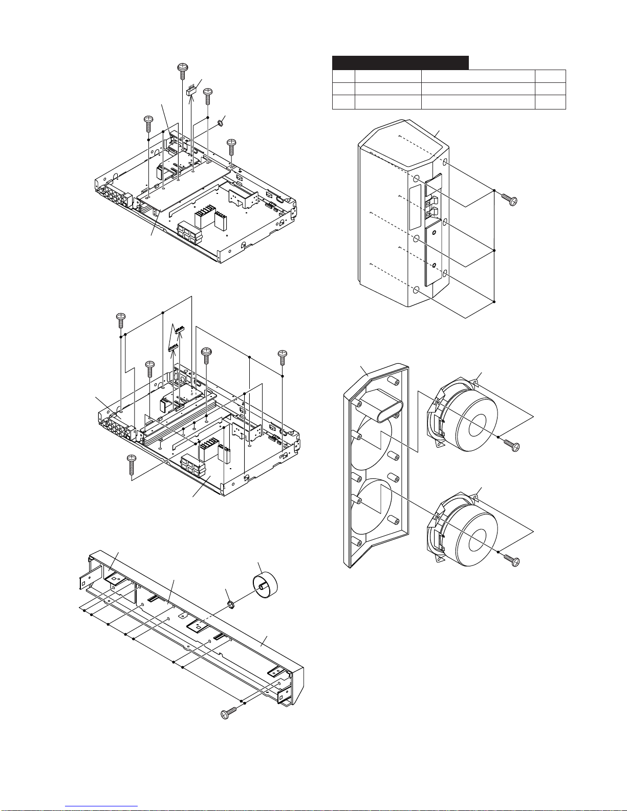
1 Top Cabinet 1. Screw ...................... (A1) x5 6-1, 2
(Note)
2 Rear Panel with 1. Screw ...................... (B1) x9 6-3
Tuner Unit 2. Flat Cable ............... (B2) x1
3. Socket ..................... (B3) x1
3 Front Panel 1. Screw ...................... (C1) x9 6-3
2. Socket ..................... (C2) x1
3. Flat Cable ............... (C3) x2
4 Heat Sink 1. Screw ...................... (D1) x6 7-1
5
Headphones PWB
1. Screw ...................... (E1) x1 7-1
2. Nut........................... (E2) x1
3. Socket ..................... (E3) x1
6 Power PWB 1. Screw .....................(F1) x13 7-2
2. Socket ......................(F2) x2
7 Main PWB 1. Screw ...................... (G1) x5 7-2
8 Display PWB/ 1. Knob........................ (H1) x1 7-3
Remote Sensor 2. Nut........................... (H2) x1
PWB 3. Screw .................... (H3) x10
DISASSEMBLY
Caution on Disassembly
Follow the below-mentioned notes when disassembling
the unit and reassembling it, to keep it safe and ensure
excellent performance:
1. Be sure to remove the power supply plug from the wall
outlet before starting to disassemble the unit.
2.Take offnylon bandsorwire holderswhere theyneedto
beremovedwhendisassemblingtheunit.Afterservicing
theunit, besure torearrange the leadswherethey were
before disassembling.
3. Take sufficient care on static electricity of integrated
circuits and other circuits when servicing.
Figure 6-2
STEP REMOVAL PROCEDURE FIGURE
Figure 6-1
Figure 6-3
SD-AT1000
(A1)x1
ø3x10mm
Rear Panel
Top Cabinet
Front
Panel
(A1)x1
ø3x10mm
(A1)x3
ø3x10mm
SD-AT1000
(C1)x3
ø3x8mm
(C1)x1
ø3x8mm
(C1)x1
ø3x8mm
(C1)x3
ø3x10mm
(B1)x9
ø3x8mm
(B3)x1
(C3)x1
(C3)x1
(C2)x1
(B2)x1
Power
PWB
Tuner Unit
Rear Panel
Front
Panel
Main PWB
(C1)x1
ø3x8mm
Top Cabinet
2
3
1
Note:
Pull the upper top cabinet toward you, and lift up one side to
remove the upper top cabinet (see arrows in the figure).

– 7 –
SD-AT1000
Figure 7-2
Figure 7-3
Figure 7-4
Figure 7-5
1-Bit Top
Heat Sink
(D1)x3
ø3x8mm
(D1)x2
ø3x8mm
(D1)x1
ø3x8mm
(E1)x1
ø3x8mm
(E2)x1
(E3)x1
Headphones
PWB
Main PWB
Power PWB
(G1)x1
ø3x12mm
(G1)x4
ø3x8mm
(F1)x3
ø3x8mm
(F1)x6
ø3x8mm
(F1)x4
ø3x16mm
(F2)x2
Remote Sensor PWB
Display PWB
Front Panel
(H3)x10
ø2.6x10mm
(H2)x1
(H1)x1
1 Front Panel 1. Screw ...................... (A1) x6 7-4
2 Speaker 1. Screw ...................... (B1) x4 7-5
STEP REMOVAL PROCEDURE FIGURE
CP-AT1000F/CP-AT1000C
Figure 7-1
(A1)x6
ø3x12mm
Speaker Box
(B1)x2
ø3x12mm
Speaker
(B1)x2
ø3x12mm
Front Panel Speaker

SD-AT1000
– 8 –
Figure 8-1
Figure 8-2
1 Front Panel 1. Screw ...................... (A1) x6 8-1
2 Speaker 1. Screw ...................... (B1) x2 8-2
STEP REMOVAL PROCEDURE FIGURE
CP-AT1000R
(A1)x6
ø3x12mm
Speaker Box
(B1)x2
ø3x12mm
Speaker
Front Panel
Figure 8-3
1 Woofer 1. Screw .................... (A1) x10 8-3
2. Subwoofer Stand .... (A2) x1
STEP REMOVAL PROCEDURE FIGURE
CP-AT1000SW
(A1)x10
ø4x20mm
Woofer
(A2)x1
Speaker Box

– 9 –
SD-AT1000
DESCRIPTION OF CIRCUIT FOR 1-BIT UNIT
(SEE THE WIRING DIAGRAMS ON PAGES 38 AND 39.)
Input section
Signalsfrom CNA100 arecoupledbyCA100,CA101,CA200,
CA300 and CA301, and then sent into the A/D converter IC
(ICA100, ICA200, ICA300).
modulation 1-bit converter
Signals from the A/D converter IC (ICA100, ICA200, ICA300)
are converted to 1-bit signals and sent differentially. Refer to
thetechnicalmanualofSM-SX100forthedetailsofconversion
to 1-bit signals.
Low pass filter circuit
1-bit signals switched by the output IC (ICA101, ICA102,
ICA201,ICA202,ICA301andICA302)areconvertedtoanalog
signals through the lowpass filter consisting of LA104 ~
LA107,LA204~LA207,LA304~LA307andCA114~CA117,
CA214 ~ CA217, and CA314 ~ CA317. The low pass filter
functionswhenafrequencyexceeds20kHz,andreducesitby
approx. 3 dB when it reaches approx. 40 kHz.
Figure 9-2
ADJUSTMENT
Figure 9-1 OUTPUT OFFSET LEVEL
1-bit amplifier's output offset voltage adjustment
Adjust VRA100, VRA101, VRA200, VRA201, VRA300 and
VRA301 so that the DC voltage between speaker terminals +
and - is set to 0 ±5 mV at AC 120 V.
Electronic
Voltage
SO889
AC 120 V
Set
Output:
Speaker Terminal
+
-
VR : 0
Input : AUX
VRA300 VRA301
VRA200 VRA201
VRA101 VRA100
POWER PWB
L-CH OUTPUT OFFSET ADJUSTMENT
R-CH OUTPUT OFFSET ADJUSTMENT
Dynamic feedback circuit
The 1-bit signals switched by the output IC (ICA101, ICA102,
ICA201, ICA202, ICA301 and ICA302) oscillate between
positive and negative voltage. After resistance-division, the
signalsare fedbacktotheA/DconverterIC(ICA100,ICA200,
ICA300) through NF resistance 75 kohms (RA155 ~ RA158,
RA255~ RA258, RA355~RA358).Thepeak-to-peakvoltage
reaches approx. 5 V.

SD-AT1000
– 10 –
TO CHECK AND CANCEL PROTECT CIRCUIT DETECTION LINE
1:Inthismodelthemicrocomputer(IC701)detectsthefollowing
malfunctions once power is supplied, and cuts off power
from all the parts except for the circuit driving the
microcomputer.
1
Abnormal drop in the output voltage of each regulator
(below approx. 1.5 V)
Power is cut off instantly without display.
2
Output offset over voltage of the 1-bit amplifier
(above approx. DC 2 V)
3
Mains overvoltage of the 1-bit amplifier
(above approx. DC 5.5 A)
Power is cut off instantly without display.
4
Defects in the cooling fan or its drive circuit
(when stopped)
Power is cut off after “FAN LOCK” is displayed.
2: Criteria for abnormality, and checking and cancelling the
detection line
The criteria:
1
The voltage of pin 2 (PROTECT) on IC701.
2
The voltage of pin 7 (OFFSET) on IC701: Low (below
approx. 1 V) (abnormal) and High (above approx. 2.5
V) (normal) .
3
The motor stops when it is above approx. 1 V.
If the voltage of pin 1 (FAN LOCK) on IC701 is not
between approx. 0.21 V and 0.9 V whilst the motor
rotation is controlled, it is judged as abnormal.
Checking and cancelling the detection line:
Caution: If the PROTECT/OFFSET detection line is
disconnected in case of
1
,
2
or
3
above, a
protective operation does not function. The
disconnection by output short-circuit of each
regulator may cause the parts or PCBs to burn
outandthereforedonotdisconnectthedetection
line when the cause is not identified.
(Power supply can be detected with an
oscilloscopeor likeduringapprox. 0.5seconds
after an abnormality is found. Note that the
detection would be difficult with a tester as the
voltage rises and falls rapidly.)
11
11
1
Abnormal drop in the output voltage of each regulator
Connect a measuring device (such as an oscilloscope) to
the stabilizing output of the regulator, and turn on the unit.
If the detected voltage is extremely lower than the voltage
on the circuit diagram (below approx. 1.5 V), the regulator
itself or the circuit is defective.
22
22
2
Output offset overvoltage of the 1-bit amplifier
Adjust the voltage of the output offset. If a protective
operation is still activated, ICA401 on the 1-bit amplifier
could be defective (the detection circuit of the speaker
output DC voltage).

– 11 –
SD-AT1000
•Schematic diagram and Wiring Side of P.W.Board for this
model are subject to change for improvement without prior
notice.
•The indicated voltage in each section is the one measured
by Digital Multimeter between such a section and the chas-
sis with no signal given.
•Parts marked with “ 1” ( ) are important for
maintaining the safety of the set. Be sure to replace these
parts with specified ones for maintaining the safety and
performance of the set.
NOTES ON SCHEMATIC DIAGRAM
REF. NO DESCRIPTION POSITION
JOG701 JOG VOLUME ON—OFF
SW701 DIGITAL ON—OFF
SW702 LINE ON—OFF
SW703 TUNER (BAND) ON—OFF
SW704 TUNING UP ON—OFF
SW705 TUNING DOWN ON—OFF
SW706 POWER ON—OFF
TYPES OF TRANSISTOR AND LED
2SB709 AR
2SD601 AR
2SK208
CPH3418
KRA106 S
KRA107 S
KRC102 S
KRC104 S
KRC107 S
KTC2875 B
2SC5565
KTC4375 Y AG01Z
AK09
DS1SS133
EK03
EK19
GD1N4004
B
(3)
E
(1)
C
(2)
BCE
TOP
VIEW
KDS120E
KDS121E
KDS226
TOP VIEW
TOP VIEWTOP VIEW
KTA1023 Y
KTA1266 GR
KTA1273 Y
KTC3199 GR
KTC3203 Y
VIEW
FRONT
E C B
VIEW
FRONT
123
(S)(G)(D)
(1)(2)(3)
SFPW56 MA111
D5SB60
AC AC
VIEW
FRONT
FRONT
VIEW
304AT2E
304BC2E9
304GT1U
304VT2E2
304VT2E3
SARS03
KRA102 M
KRC102 M
KRC104 M
KRC106 M
KRC107 M
VIEW
FRONT
Cathode Anode
FMLG22S
1. Anode
2. No Contact
3. Cathode
•Resistor:
To differentiate the units of resistors, such symbol as K and
M are used: the symbol K means 1000 ohm and the symbol
M means 1000 kohm and the resistor without any symbol is
ohm-type resistor. Besides, the one with “Fusible” is a fuse
type.
•Capacitor:
To indicate the unit of capacitor, a symbol P is used: this
symbol P means pico-farad and the unit of the capacitor
without such a symbol is microfarad. As to electrolytic
capacitor, the expression “capacitance/withstand voltage”
is used.
(CH), (TH), (RH), (UJ): Temperature compensation
(ML): Mylar type
(P.P.): Polypropylene type

SD-AT1000
– 12 –
Figure 12 BLOCK DIAGRAM (1/10)
+12V +12V
A_+9V
A_+9V
80
79
78
77
76
75
70
67
38
37
36
35
32
29
28
27
26
25
5678
43 1
432 1
56 78
24 23 22 21 19 17
89
101113141516
12347
48 49 50 51 52 53 54 55 5741 44 45 46 47
P_CONT_LEVEL
LINE3_LCH
LINE3_RCH
LINE1_RCH
LINE2_RCH
LINE2_LCH
LINE1_LCH
OUT_L
CONFIG
+B_CHECK
UCON5V
RIN
LIN
LOUT2
ROUT2
LOUT1
ROUT1
ROUT3
LOUT3
H.P_SW
CONFIG
CCB_DI
CCB_CL
CCB_DO
CCB_CE
FUN_LOCK
BASS_SW
VOL_CL
VOL_DA
OFFSETPROTECT
A/D_RESET
S_MUTE
S_S_MUTE
C_S_MUTE
F_S_MUTE
W_S_MUTE
L_MUTE
OUTSR_RCH
OUTC
OUTSW
OUTSR_LCH
S_MUTE
MON_OUTR
MON_OUTL
OUT_R
VOL_CL
VOL_DA
TUN_L
TUN_R
PROTECT
PROTECT
9V
LINE1 OUT
D_+5V
L
_
SW
LINE 2
LINE 1 IN
LINE 3
R-CH
L-CH
L-CH
R-CH
R-CH
L-CH
L-CH
R-CH
CENTER
GND(U-COM)
AGND2
AGND1
IN DSPSL
INDSPC
IN DSPSW
OUTSL
OUTSR
OUTSW
OUTC
IN2DSP
OUT1(+)
IN DVDSR
VCC
DA
IN1MIX
CL
MUTE OUT2(+)
INDVD SW
AGND5
AGND6
VEE
AGND4
DGND IN1DSP
INDVDC
IN DVDSL
AGND8 IN81
IN72
IN71
IN62
OUT2
OUT1
IN61
IN41
IN42
IN32
IN21
AGND9
IN12
IN11
ROUT32
ROUT31
AGND10
AGND3
AGND7
IN22
IN DSPSR
IN2MIX
IN31
14
16
15
17
18
20
13
19
21
22
12
11
10
7
23
8
9
24
6
4
5
3
2
1
25
26
27
R_CH
L_CH
H.P SW
D_GND
A_GND
PROTECT
D_+5V
D_GND
L-CH
H.P SW
A_GND
R-CH 1
3
4
5
6
1
2
3
4
5
1
2
3
4
5
A_+9V
VDD
VSS
+
+ –
–
+
–
VDD
–
+
VSS
3
4
5
6
7
8
9
10
13
11
1
CNP701
TO DISPLAY PWB TO DSP SECTIONTO DSP SECTIONTO DSP SECTION
+B
BI601
CNS601
JT501
LINE1 INPUT/
OUTPUT TERMINAL
JT502
LINE2/LINE3
INPUT TERMINAL
Q528 Q501
Q532
Q533
Q531
Q504
Q503
Q599
Q598
Q502
IC520
TJM4558CD
OPE AMP.
IC505
NJM4565M
BUFFER AMP.
CNP501
IC501
BD3811K1
VOLUME IC
D538
D537
CNP601
JK1
HEADPHONES

– 13 –
SD-AT1000
Figure 13 BLOCK DIAGRAM (2/10)
–15V(A)
+12V(A)
D_+5V
D_+5V
M_+12V
+15V(A)
A_–8.2V
A_+8.2V
31
8
4
31
8
4
8
4
8
4
CNP506
432 1
56 78
321
67
5
321
567
765
32 1
2
2
321
567
FAN_LOCK
P_CONT_LEVEL
+B_CHECK
PROTECT
UCON_+5V
FAN_CONT
WOOFER_OUT
TUN_R
TUN_L
A_GND
L_MUTE
S_MUTE
A_+7V
A_–7V
D_+5V
OFFSETPROTECT
A/D_RESET
PROTECT
W_S_MUTE
FRONT_LCH
R_CH
L_CH
F_S_MUTE
BASS_SW
OUTSR_LCH
OUTSR_RCH
OUTC
FRONT_RCH
OUTSW
C_S_MUTE
S_S_MUTE
CCB_DO
CCB_CL
CCB_DI
CCB_CE
A_–7V
LIMIT
D2_GND
GND
D_+5V
SUBWOOFER
OUT
M_+12V
M
PROTECT
TO TUNER UNIT
A_–12V
A_+12V
L_MUTE
S_MUTE
GND
UCON_GND
GND_A
M_GND
A+15V
A-15V
+15V(A)
CE
DO
GND
L OUT
VCC +9V
DI
CL
R OUT
9
13
12
11
10
8
7
6
3
4
1
2
5
1
2
2
4
7
5
1
9
3
11
6
8
10
SURROND R-CH
SURROND L-CH
FRONT L-CH
CENTER
FRONT R-CH
SUB
WOOFER
12
6
10
11
1
8
4
9
5
7
3
2
12
6
10
11
1
8
4
9
5
7
3
2
3
1
2
3
VSS +
+
–
–
VDD
–
–
+
+VSS
VDD
VDD
VSS
+
+
–
–
+VSS
VDD
–
–
+
+
–
VDD
–
+
VSS
CNS931
FROM POWER SECTION
CNA100
FROM 1-BIT SECTION
+B
-B
IC411
TJM4558CD
OPE AMP.
IC412
TJM4558CD
OPE AMP.
Q532
Q533
Q531
Q599
Q598
Q514
Q525
Q527
Q526
Q402
Q401
Q400
Q403
Q518
Q517
Q516
Q523
Q537
Q536
Q538 Q539
Q530
Q541
Q542
Q543
Q544 Q545
Q524
Q513
Q512 Q515
Q459
Q428
Q429
Q535
IC413
TJM4558CD
OPE AMP. ZD567
5
M
A
MP.
D517
D581
CNP531
D514
D507
D509
IC507
KIA7805AP
VOLTAGE
REGULATOR
D401
R402 D400
CNP401
CNS401
IC513
KIA7809AP
VOLTAGE
REGULATOR
SO501
IC506
TJM4558CD
OPE AMP.
M501
FAN MOTOR
BI500
CNS500

SD-AT1000
– 14 –
Figure 14 BLOCK DIAGRAM (3/10)
+5V(A)
+5V(A)
+5V(A)
+5V(D)
+3.3V(D)
SI3050LUS
3
1
AK4586VQ
43
42
41
40
38
36
34
22 21 20 19 18 17 16 15 14 13 12
8
4321
2
11
10
9
1
2
3
4
5
6
7
8
33
32
31
30
29
28
27
26
23
OVF
COD_DO
COD_DI
COD_CLK
COD_CSN
DSP_SCCLK
DSP_CS
DSP_SCDIN
DSP_SCDOUT
DSP_RESET
DSP_INTREQ
DIG_FUNC+B
NONPCM
COD_CSN
COD_DO
D_+5V
A_GND
A_+9V
LOUT3
ROUT3
LOUT2
ROUT2
LOUT1
ROUT1
LIN
RIN
DGND
PROTECT
NONPCM
COD_CLK
OVF
COD_DI
PROTECT
EX_CLK
MCLK
LRCK
AUDATA0
SCLK
SDATA1
AUDATA2
AUDATA1
VCC
GND
3Y
2A
1A
12
ADC/DAC/DIR
CONVERTER
PVDD
PVSS
SLAVE
TST
RX2
I2C
RX1
CAD0/CSN
SCL/CCLK
SDA/CDTI
CAD1/CDTO
INT1
INT0
MCKO
TX
XTI/EXTCLK
XTO
DZF2/OVF
VREFH
AVDD
AVSS
LIN
RIN
ROUT1
ROUT2
ROUT3
LOUT3
LOUT2
LOUT1 DVSS
DVDD
TVDD
SDTO
SDTI3
SDTI2
SDTI1
LRCK
BICK
15
14
12
11
10
9
8
7
6
5
4
3
2
1
13
CNP702
TO DISPLAY SECTION
13
12
11
10
9
8
7
6
5
4
3
2
1
TO MAIN SECTION
IC110
VOLTAGE
REGULATOR
D103
IC102
RX101
OPTICAL
DIGITAL IN
Q102
T
D
U
N
A
D104
CNP502
VOLTAGE
REGULATOR
IC109
TC7WU04U
DUAL2-INPUT
NAND GATE

– 15 –
SD-AT1000
Figure 15 BLOCK DIAGRAM (4/10)
+5V(A)
+2.5V(D)
+3.3V(D)
+3.3V(D)
+3.3V(D)
+2.5V(A)
+2.5V(A)
+2.5V(A)
+2.5V(A)
IX0446AW
3
1
SI3033LUS
3
1
8
7
6
4321
14 13 12 11 9 8
7
6
5
4
3
2
1
CS493264
44
43
42
41
40
28 27 26 25 24 23 22 21 20 19 18
6
5
4
2
1
22
39
36
35
34
30
29
7
8
9
10
11
12
13
14
15
16
17
DSP_SCCLK
DSP_INTREQ
_DSP_INTREQ
EX_CLK
_DSP_SCDOUT
_DSP_CS
_DSP_SCDIN
DSP_SCDIN
DSP_SCDOUT
DSP_CS
_DSP_SCCLK
DSP_RESET
LRCK
SCLK
MCLK
AUDATA1
AUDATA0
_DSP_SCDIN
/EMWR
/EMOE
/EXTMEM
EMAD0
EMAD1
_DSP_INTREQ
_DSP_SCDOUT
_DSP_CS
_DSP_SCCLK
EMAD5
EMAD3
EMAD6
EMAD4
EMAD7
EMAD2
AUDATA2
LRCK
SDATA1
SCLK
LRCK
SCLK
SDATA1
12.288 MHz
DSP
1A
1Y
2A 3A
3Y
GND
VCC
SCLKN2
LRCLKN2
SDATAN2
SCCLK
SCDIN
SCDOUT
CS
INTREQ
EXTMEM
SDATAN1
SCLKN1
LRCLKN1
D0
D1
D2
D3
D4
D5
D6
D7
RD
WR
MCLK
SCLK
LRCLK
AUDATA0
AUDATA1
AUDATA2
CLKIN
RESET
AGND
VA
DGND3
DGND2
DGND1
VD3
VD2
VD1
VCC
GND
IC103
TC7WU04U
DUAL2-INPUT
NAND GATE
IC104
74HC07AF
BUFFER AMP.
IC111
IC112
D104
D105
ZD101
IC101
XL101
VOLTAGE
REGULATOR
3.3V
REGULATOR

SD-AT1000
– 16 –
Figure 16 BLOCK DIAGRAM (5/10)
IX0558AW
100
98
97
96
95
94
93
92
91
90
89
88
87
86
85
84
83
82
81
12 56789101112 2322212019181716151413 3433323130292827262524 35
80 79 78 77 76 75 74 73 72 71 70 60616263646566676869 5859
1234 6789 1516 232221201918
POWER_LEVEL1
1G
2G
3G
4G
5G
6G
7G
8G
9G
10G
11G
12G
F1
F1
13G
P1
P2
P3
P4
P5
P6
P7
P8
P9
P10
P11
P12
P13
P14
P15
P16
14G
15G
SYSTEM MICROCOMPUTER
VSS
CCB DI
CCB CL
RESET
CCB_DO
CCB_CE
POWER_LEVEL2
OFF_SET
A/D_RESET
FAN_LOCK
JOG
PROTECT
+B_CHECK
TIMER LED
GND
S_MUTE
S_S_MUTE
C_S_MUTE
F_S_MUTE
W_S_MUTE
L_MUTE
SEG8
SEG16
SEG15
SEG14
SEG13
SEG12
SEG11
SEG10
SEG9
SEG7
SEG6
SEG5
SEG4
SEG3
SEG2
SEG1
DIG15
DIG14
DIG7
DIG8
DIG6
DIG5
DIG4
DIG3
DIG2
DIG1
DIG9
KEY1
VEE
DIG10
DIG11
DIG12
DIG13
VREF
X_IN
X_OUT
VF1
3
1
4
5
6
2
1
3
4
5SP_RELAY
–VP FOR FL
VF2
AC_RELAY
P_CONT_LEVEL
9V
H.P_SW
CONFIG
CCB_CL
CCB_DO
CCB_CE
OFF_SET PROTECT
A/D_RESET
+B_CHECK
PROTECT
VOL_CL
VOL_DA
D_GND
SW 5V
BASS_SW
14151617181920 13 12 11 10 7 2485639
CCB_DI
27 26 25 24 23 22 21
L_MUTE
W_S_MUTE
F_S_MUTE
C_S_MUTE
S_S_MUTE
FAN_LOCK
S_MUTE
CNP901
TO POWER SECTION
CNP501
TO MAIN SECTION
TO POWER SECTION
BI701
CNS701
FL701
FL DISPLAY
XL701
4.19 MHz
LED701
JOG701
JOG VOLUME
SW706
POWER
QS01 QS02
QS08QS07QS06
QS03QS04QS05
IC701
SW705
TUNING
DOWN
SW704
TUNING UP
SW703
TUNER
(BAND)
SW702
LINE
SW701
DIGITAL

– 17 –
SD-AT1000
Figure 17 BLOCK DIAGRAM (6/10)
50
49
48
47
46
45
44
43
42
41
40
38
37
36
35
34
33
32
31
PST9140
21
GP1UM271 21
BLUE
3
343332 393835
6061 5152535455565859
232221 302927262524
3
+5V(UNSWD)
+5V(BACK UP)
BASS SW
CONFIG
RX-IN
F2
F1
P13
P14
P15
P16
DIG FUNC
E
R
DPL_LED
DD_LED
POWER_KEY
VSS
VCC
DIMMER
DSP_INTREQ
DSP_CS
DSP_SCCLK
DSP_SCDIN
DSP_SCDOUT
DSP_RESET
OVF
STD_LED
DTS_LED
SURR_LED
STEREO_LED
COD_DO
COD_CLK
COD_DI
COD_CSN
VOL_DA
VOL_CL
AC RLY
SP_RLY
NONPCM
SEG16
SEG15
SEG14
SEG13
SYS_STOP
X_IN
X_OUT
4
2
11
2
4
1
3
5
3
655
43
GND
DSP_SCCLK
COD_CSN
COD_CLK
DSP_RESET
DSP_CS
DSP_SCDIN
DSP_SCDOUT
DSP_INTERQ
OVF
COD_DO
COD_DI
DIG_FUNC_+B
NON_PCM
15
14
13
10
9
8
7
6
5
4
3
2
1
11
12
9V
CONFIG
D_GND
UN_SW 5.6V
SW 5V
BASS_SW
245613
CNP502
TO MAIN SECTION
RESET
LED
DRIVER
LED
DRIVER
LED
DRIVER
LED
DRIVER
LED
DRIVER
LED
DRIVER
XL701
4.19 MHz
LED706
LED705
LED704
LED703 LED708
LED707
RM709
LED702
BI702
CNS702
CNP705
D702
D701
Q701
Q703
Q704
Q705
Q706
Q707
Q708
Q709
Q710
Q702
IC703
RESET
CNP702
CNP701
REMOTE SENSOR

SD-AT1000
– 18 –
Figure 18 BLOCK DIAGRAM (7/10)
D1_GND
D_+5V
A1_GND
AC_RELAY
FL–
FL+
VP
SP_RLY
PWR_GND
GND
D2_GND
A_GND
A_+15V
A_–15V
M_GND
2
1
3
AK09
AC POWER SUPPLY CORD
AC 120 V, 60 Hz
FB/SYNC
SYNC
OCP
GND
Vin
Drain
5 42 1
3
3
2
1
12
13
89
1014
12345
A_+5V
1354
1243
3
2
1
1bit_PWR_GND
1bit_+40V
1bit_DRIVER_+9V
DRIVER_+9V
TO 1-BIT AMP. SECTION
11
12
789
13
161514
CNS701
FROM DISPLAY SECTION
CNA104
TO 1-BIT AMP. SECTION
C
TO MA
I
11
22
IC901
STRF6229
SWITCHING REGULATOR
Q931
Q895
Q895
Q932
D902
D943
BI933
CNS933
T901
SWITCHING
POWER TRANSFORMER
D960
CNP901
D944
L931
IC933
KIA7809AP
VOLTAGE
REGULATOR
IC931
SE-B2
ERROR
AMP.
D936
D901
PC901
TH901
D942
D930
D939
D938
D945
D957
IC934
KIA7805AP
VOLTAGE
REGULATOR
PS932
PS931
F901
8A/125V
L901 L902
AC LINE
FILTER
AC LINE
FILTER

– 19 –
SD-AT1000
Figure 19 BLOCK DIAGRAM (8/10)
+40V
R-CH –
L-CH –
L-CH +
L-CH –
R-CH –
L-CH +
R-CH +
R-CH +
UCON_GND
M_+12V
LIMIT
FAN_CONT
SP_RLY
SUB_W–_IN
SUB_W+_IN
CENT+_IN
CENT–_IN
SR+_IN
SR–_IN
SL+_IN
SL–_IN
FL +
FL –
FR –
FR +
SL +
SL –
SR –
SR +
SP__RLY
SP__RLY
SP_RLY
SP__RLY
3
2
1
1 BIT AMP
5
6
7
8
4
3
2
1
AC_RELAY
CENT –
CENTER
SUBWOOFER
CENT +
WOOFER +
WOOFER –
SURROND
FR+_IN
FR–_IN
FL–_IN
FL+_IN
FRONT
UCON_+5V
PROTECT
+B_CHECK
43 5
1
11
WOOFER +
WOOFER –
CEN +
CEN –
CENTER
678
10
9
11
12
5
SL +
SL –
SR +
SR –
FR +
FL +
FL –
FR –
2134
SURROUND FRONT
SUBWOOFER
76
324
1
10
65
17 18 19 20 21 22 23 24 25 26 27 28
TO 1-BIT AMP. SECTION
CNP531
TO MAIN SECTION
D887
D963
Q951
Q950
Q892
PC902
ZD937
IC306
TJM4558CD
OPE AMP.
BI931
CNS931
RL897
RL898
RL899
D954
D953
GD1N4004 D951
GD1N4004
D952
GD1N4004
D950
GD1N4004
IC937
AN77L05
VOLTAGE
REGULATOR
D891 D890
D889
PC901
T903
POWER TRANSFORMER
D947
SO889
SPEAKER
TERMINAL
VDD
VSS
+
+ –
–

SD-AT1000
– 20 –
Figure 20 BLOCK DIAGRAM (9/10)
SLA
5
SLA5515M
123
4321
11
13
1234
5
6
7
8
9
101112
13 14 15 16 17 20 21 22 23 24
1
2
3
4
5
6
9
10
11 13
12
15
16
17
18
19
20
21
14
9
10
11
6
5
4
3
2
1
9
10
11 13
12
15
16
17
18
19
20
21
14
6
5
4
3
2
1
1
2
3
7
6
5 8 4
D+5V
AMP_VCC
D+5V
+B_AMP
A+5V
R-CH_1
L-CH_1
PWR_GND
A+5V
AGND_AD
DGND_AD
D+5V
OUTA
VBBA
INA
VBBA
OUTA
VBOO
T
V
SA
VCC
VKK
VKKVCC
VKK
GND
SBSA
OUTB
OUTB
VBBB
VBBB
VDD
INB
VBOOTB
VBOOTA
INA
VBBA
VBBA
OUTA
OUTA
L-CH_IN 1
AGND 1
R-CH_IN 1
Lch_+1
Lch_-1
Rch_-1
Rch_+1
Rch_-2
Rch_+2
DRIVER_+9V
+40V
TEST
NFR1(+)
NFL2(–)
NFL1(+)
NFR2(–)
GNDA
R-CH IN
L-CH IN
RESET
VDA VDDL
GNDD
OUTL(+)
OUTL(–)
OUTR(–)
OUTR(+)
VDDR
VDDL
VDDX
XI
XO
GNDX
MCK
ANALOG IN R-CH ANALOG IN L-CH
VKKVCC
VKK
GND
SBSA
OUTB
OUTB
VBBB
VBBB
INB
VBOOTB
VDD
VBOOTA
INA
VBBA
VBBA
OUTA
OUTA
ANALO
G
GNDX TEST
11.2896 MHz
–
+
–
+
3
1
2
2
1
3
3
1
2 2
1
3 2
3 1
CNS933
FROM POWER SECTION
14 16 15 25 26 28 27 17 18
FRONT SUBWOOFE
R
TO POWER SECTION
R-CH OUTPUT
OFFSET
ADJUSTMENT
L-CH OUTPUT
OFFSET
ADJUSTMENT
LFA200
DA116 DA107
DA400
DA402
DA401
DA403
PSA400
PSA402
PSA401
ICA102
SLA5515M IC
A
ICA101
ICA401
TJM4558CD
OPE AMP.
QA414
QA416
QA402 QA401 QA400
QA415
DA404
CXA100
VRA101
VRA100
LFA403
CNA104
LFA402
LFA400
LFA100
LFA101
ICA200
IX0498AW
SWITCHING
AUDIO
POWER AMP.
SWITCHING
AUDIO
POWER AMP.
SWIT
C
AU
D
POWE
R
ICA100
IX0498AW
7TH ORDER ∆∑
MODULATION
CONVERSION LSI
7TH ORDER ∆∑
MODULATION
CONVERSION LSI
Other manuals for SD-AT1000
2
Table of contents
Other Sharp Home Cinema Speakers manuals