SiTime SiT15 Series User manual

The Smart Timing Choice™ 1 SiT-AN10037 Rev 1.3
Oct 2014
Optimized SiT15xx Drive Settings for
32 kHz Crystal Inputs of Low Power MCUs
Table of Contents
1Introduction ............................................................................................................................................2
2MCU 32 kHz Oscillator Operating Modes..............................................................................................2
3SiT15xx Output Drive Levels .................................................................................................................4
3.1 NanoDrive Reduced Swing Mode.................................................................................................4
3.2 Full-Swing LVCMOS Drive............................................................................................................5
4Energy Micro EFM32.............................................................................................................................6
5STMicroelectronics STM32....................................................................................................................6
6Renesas Electronics RL78G13..............................................................................................................7
7Texas Instruments MSP430F2x ............................................................................................................7
8NXP LPC11xx........................................................................................................................................8
9Freescale Kinetis L4x/L5x......................................................................................................................8
10 Appendix A: Programming the EnergyMicro EFM32 LFXO..............................................................9
10.1 EFM32 Clock Management Unit...................................................................................................9
10.2 Configuring the LFXO .................................................................................................................12
11 Appendix B: Programming the STMicroelectronics STM32 LSE Oscillator....................................13
11.1 Low-speed External Clock Oscillator ..........................................................................................13
11.2 External Clock Source (LSE bypass)..........................................................................................14
11.3 Clock Security System on LSE ...................................................................................................14
11.4 Clock-out Capability ....................................................................................................................14
11.5 Configuring LSE..........................................................................................................................15
12 Appendix C: Programming the Renesas Electronics RL78G13 XT1 Oscillator..............................16
12.1 XT1 Oscillator..............................................................................................................................16
12.2 Configuration XT1 .......................................................................................................................16
13 Appendix D: Programming the Texas Instruments MSP430 Low Frequency Oscillator ................18
13.1 The MSP430 LFXT Oscillator .....................................................................................................18
13.2 Clock-out Capability ....................................................................................................................20
13.3 Low-power Modes.......................................................................................................................20
14 Appendix E: Programming the NXP LPC1100 RTC Oscillator.......................................................21
14.1 Configuring of the RTC Oscillator ...............................................................................................21
14.2 Clock Output Capability...............................................................................................................21
15 Appendix F: Programming the Freescale Kinetis L4x and L5x System Oscillator..........................28
15.1 Programming Model....................................................................................................................28
15.2 Clock Output Capability...............................................................................................................34

The Smart Timing Choice™ 2 SiT-AN10037 Rev 1.3
SiT15xx Optimized Drive Settings
1 Introduction
Embedded microcontroller (MCU) based systems have historically relied on a low frequency
32.768 kHz quartz resonator driven oscillator for time keeping and failure recovery functions.
TempFlat™ MEMS SiT153x oscillators and SiT155x temperature compensated oscillators
(TCXOs) are a new generation of smaller footprint 32.768 devices that offer a cost effective,
more reliable, improved frequency stability alternative to quartz-based 32.768 kHz oscillators.
This application note gives an overview of on-chip 32 kHz oscillator modes used in low power
MCUs and the different drive settings supported by the SiT15xx families. The SiT15xx devices
feature NanoDrive™, a factory programmable output voltage swing to optimize power and
connectivity to existing oscillator sustaining circuits. This document lists valid combinations of
SiT15xx output drive VOH/VOL settings and the associated part number for specific MCUs.
A list of SiT15xx drive settings optimized for each of the 32 kHz oscillator modes is provided for
the following MCUs:
1. Energy Micro EFM32
2. Renesas Electronics RL78G13
3. STMicroelectronics STM32
4. Texas Instruments MSP430F2x
5. NXP LPC11xx
6. Freescale Kinetis L4x/L5x
The programming details specific to each MCU are listed in individual Appendices at the end of
this application note.
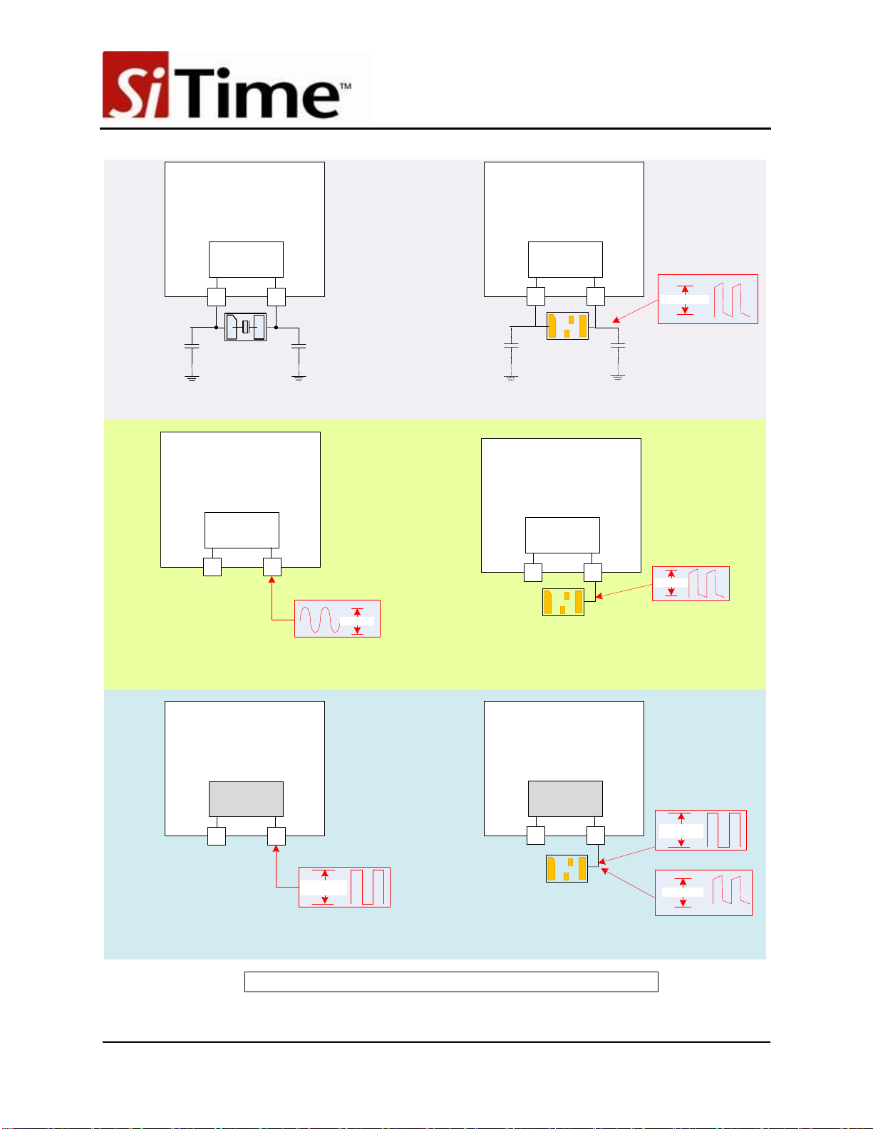
2 MCU 32 kHz Oscillator Operating Modes
Most energy efficient MCUs implement on-chip 32.768 kHz oscillators as a variant of a Pierce
oscillator with either fixed or adjustable inverting gain stage as show in Figure 1.
Variable Gain
Inverting Amplifier Level
Translator
Crystal IN
(XIN) Crystal OUT
(XOUT)
C1 C2
Rf
Rs To downstream
receiver
Figure 1: Typical 32.768 kHz oscillator block diagram shown with a crystal resonator.
This low frequency oscillator can be configured to operate in three distinct modes as shown in
Figure 2.
1. Mode-1: Resonator only mode: drives a 32.768kHz quartz resonator
2. Mode-2: Accept a sine wave input ≥200 mVpp on XIN pin
3. Mode-3: Digital logic level clock input after bypassing or shutting off the on-chip
oscillator. For oscillator inputs compatible to 1.8V logic levels, a smaller swing
NanoDrive supported by the SiT15xx can be leveraged to save additional power.
The Smart Timing Choice™ 3 SiT-AN10037 Rev 1.3
SiT15xx Optimized Drive Settings
XOUT XIN
SiT153x
MCU
C2 C1
XOUT XIN
32.768 kHz
Oscillator
(Enabled)
MCU
C2 C1
32.768 kHz
Oscillator
(Enabled)
12
43
VDD
GND CLK OUT
XOUT XIN
SiT153x
MCU
XOUT XIN
32.768 kHz
Oscillator
(Enabled)
MCU
(Mode-2) Oscillator ON and driven by external sine wave signal
32.768 kHz
Oscillator
(Enabled)
12
43
VDD
GND CLK OUT
XOUT XIN
SiT153x
MCU
XOUT XIN
32.768 kHz
Oscillator
(Disabled)
MCU
32.768 kHz
Oscillator
(Disabled)
12
43
VDD
GND
(Mode-2) Oscillator ON and driven by SiT153x NanoDrive output
(Mode-1) Oscillator ON and driven by external quartz resonator (Mode-1) Oscillator ON and driven by SiT153x NanoDrive output. C1
and C2 are optional and can be removed for additional power savings
(Mode-3) Oscillator OFF/Bypassed and driven
by external logic level square wave signal
(B)
(C)
(A)
250 mV
(Mode-3) Oscillator OFF/Bypassed and driven by SiT153x
CMOS drive or NanoDrive for 1.8V logic level inputs
1.2-3.3V
250 mV
1.2-3.3V
OR
250-800 mV
**
* - C1 and C2 are optional and can be de-populated for additional power savings.
800 mV
Figure 2: Operational modes of an MCU on-chip 32 kHz oscillator.

The Smart Timing Choice™ 4 SiT-AN10037 Rev 1.3
SiT15xx Optimized Drive Settings
3 SiT15xx Output Drive Levels
The SiT15xx devices support two distinct output drive modes.
1. NanoDrive™ reduced swing, factory programmable
2. Rail-to-rail full-swing LVCMOS
3.1 NanoDrive Reduced Swing Mode
In NanoDrive mode, the SiT15xx output driver achieves various voltage swings and common-
mode bias voltages similar to drive levels sustained by various implementations of a 32 kHz
quartz crystal driven Pierce oscillator. Both DC coupled and AC coupled modes are supported.
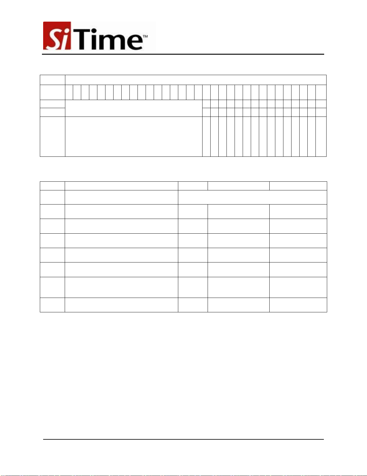
DC coupled VOH/VOL drive levels shown in Table 1 are supported for 32 kHz oscillator circuits
sensitive to DC bias and swing levels. The correct part number designator is shown inside each
VOH/VOL combination in cell in Table 1. For example SiT15xxAI-H4-D26-32.768 will provide
typical drive levels: VOH = 1.225V and VOL = 0.525V. The applicable oscillator operating
modes for this setting is Mode-1 as illustrated in Figure 2.
Table 1: Matrix of Permitted DC Coupled VOH/VOL NanoDrive Levels
VOL\VOH
1.225
1.100
1.000
0.900
0.800
0.700
0.600
0.800
D28
D18
D08
0.700
D27
D17
D07
D97
0.525
D26
D16
D06
D96
D86
0.500
D25
D15
D05
D95
D85
D75
0.400
D14
D04
D94
D84
D74
D64
0.350
D13
D03
D93
D83
D73
D63
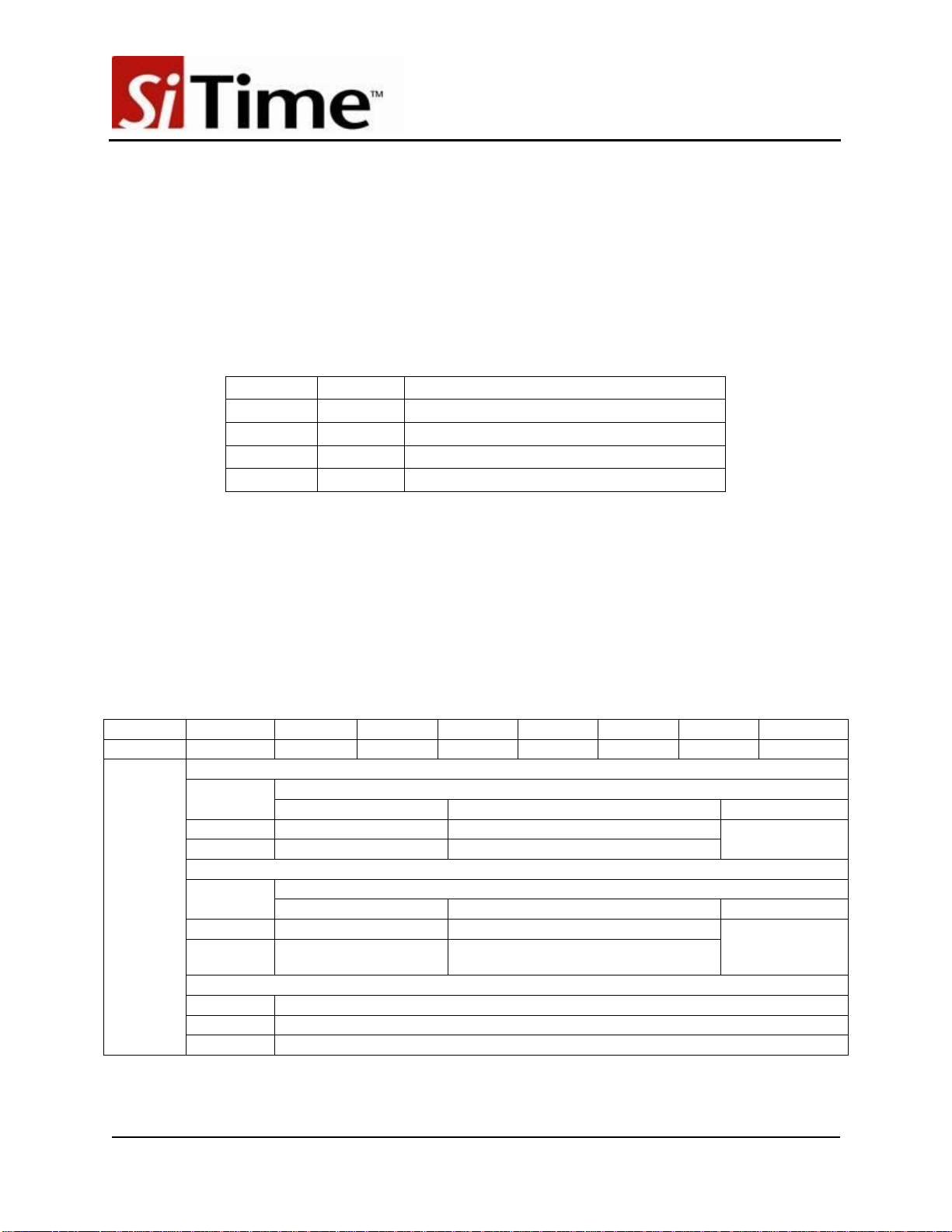
The supported AC coupled settings shown in Table 2 should be used with 32 kHz oscillator
modes which are insensitive to DC bias levels, thus only the NanoDrive swing is relevant. The
part number designator for each valid AC-swing level is shown below the valid swing option in
Table 2. For example SiT15xxAI-H4-AA4-32.768 will provide a 400mV typical voltage swing.
This AC coupled setting is most appropriate for oscillator Mode-2 as illustrated in Figure 2.
Table 2: Matrix of Permitted AC Coupled Swing Levels
Swing
0.800
0.700
0.600
0.500
0.400
0.300
0.250
0.200
Part# Output Code
AA8
AA7
AA6
AA5
AA4
AA3
AA2
AA1
The values listed in Tables 1 and 2 are typical numbers at 25°C and will exhibit a tolerance of
+/- 55 mV across VDD and operating temperature range of -40 to 85°C.
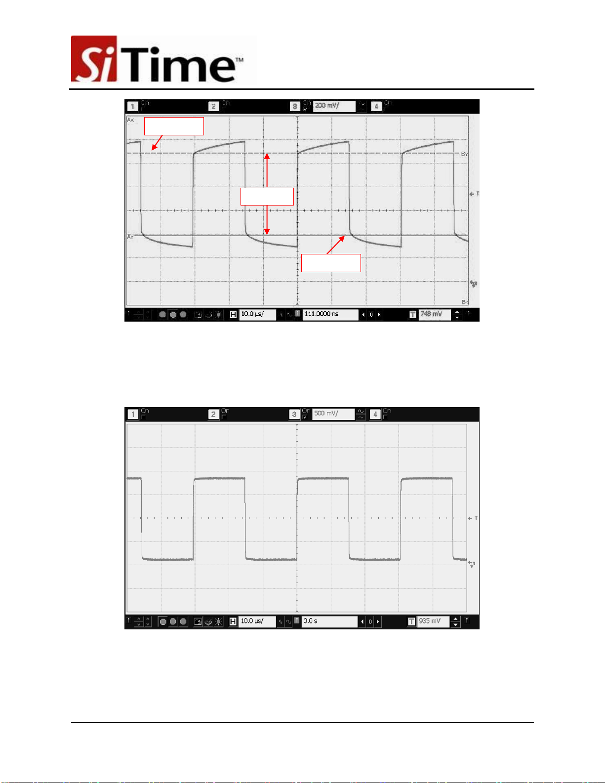
Figure 3 shows a typical waveform output of a SiT15xx oscillator when programmed in
NanoDrive mode: swing voltage, Vswing = 0.7 V, VOH = 1.1V, VOL = 0.4V in to a 15 pF load.
The corresponding part number for a 2012 package 32.768 kHz device is SiT15xxAI-H4-D14-
32.768.
The Smart Timing Choice™ 5 SiT-AN10037 Rev 1.3
SiT15xx Optimized Drive Settings
Figure 3: Scope capture of a SiT15xxAI-H4-D14-32.768 output waveform in to a 15 pF load.
3.2 Full-Swing LVCMOS Drive
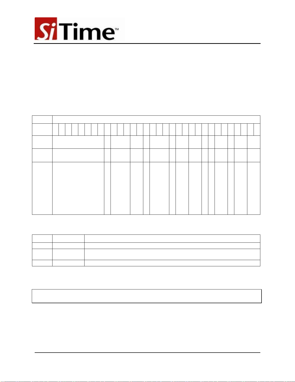
SiT15xx families can be programmed to generate full-swing LVCMOS levels. Figure 4 shows
the waveform of SiT15xxAI-H4-DCC-32.768, 1.8V VDD at room temperature in to a 15 pF load.
Figure 4: LVCMOS waveform of a SiT15xxAI-H4-DCC-32.768 at 1.8V VDD in to 15 pf load.
LVCMOS level setting should be used if the NanoDrive settings do not achieve the expected
results and best results, and lowest power, will be achieved when the on-chip oscillator has
been bypassed or disabled as illustrated for oscillator Mode-3 in Figure 2.
VOH = 1.1V
VOL = 0.4V
Vsw= 0.7V

The Smart Timing Choice™ 6 SiT-AN10037 Rev 1.3
SiT15xx Optimized Drive Settings
4 Energy Micro EFM32
The EFM32 family of microcontrollers is based on the ARM Cortex-M0, M3 or M4 processor
core targeted for low power operation. The EFM32 incorporates a low frequency crystal driven
oscillator (LFXO) for clocking on-chip peripherals (including RTC) and potentially the CPU core.
The LFXO can operate from a 32.768 kHz quartz crystal connected across the LFXTAL_N and
LFXTAL_P pins or an external clock source on the LFXTAL_P pin.
By default the low frequency crystal oscillator (LFXO) is disabled. Table 3 lists the optimal
settings of SiT15xx devices for each of the three operating modes of the LFXO oscillator.
Table 3: SiT15xx Configuration for the Three EFM32 LFXO Oscillator Modes
Mode-1: LFXO
Enabled
Mode-2: LFXO
Enabled with Sine
Wave Input
Mode-3: LFXO Disabled
LFXTAL_N, P
connections
SiT15xx,
pin-3 LFXTAL_N
SiT15xx,
pin-3 LFXTAL_N
SiT15xx, pin-3 LFXTAL_P
SiT15xx Output
Drive Settings
NanoDrive: D74
NanoDrive: AA2
LVCMOS: DCC for MCU VDD >/= 1.8V
NanoDrive: D26 for MCU VDD = 1.8V
(recommended for lowest power)
Appendix A provides details on how to enable, disable and program various operating modes of
the EFM32 LFXO oscillator.
5 STMicroelectronics STM32
The STM32L152RBT6 is an ARM-based Cortex-M3 MCU. The internal RTC has a separate
accurate low frequency (LSE) oscillator. The LSE oscillator has the advantage of providing a low
power but highly accurate clock source for the real-time clock (RTC), peripheral clock/calendar or
other timing functions. The oscillator incorporates OSC32_IN and OSC32_OUT pins for crystal
connection. As an option, an external clock source can be routed directly to the OSC32_IN pin
after bypassing the on-chip oscillator by settings the MCU registers. By default the LSE oscillator
is switched off. Unlike the EFM32, the LSE oscillator supports two operating modes. Table 4 lists
the optimal settings of SiT15xx for each of the two operating modes of the LSE oscillator.
Table 4: SiT15xx Configuration for the Two STM-32 LSE Oscillator Modes
Mode-1: LSE
Enabled
Mode-2: LSE
Enabled with Sine
Wave Input
Mode-3: LSE Disabled
LFXTAL_N, P
connections
SiT15xx,
pin-3 OSC32_IN
Not Supported
SiT15xx, pin-3 OSC32_IN
SiT15xx Output
Drive Settings
NanoDrive: D13
Not Applicable
LVCMOS: DCC for MCU VDD >/= 1.8V
NanoDrive: D26 for MCU VDD = 1.8V
(recommended for lowest power)
Appendix B provides details on how to enable, disable and program various operating modes of
the STM32 LSE oscillator.

The Smart Timing Choice™ 7 SiT-AN10037 Rev 1.3
SiT15xx Optimized Drive Settings
6 Renesas Electronics RL78G13
The R5F100LE is a 16-bit MCU based on the RL78 core. The MCU includes a low frequency
crystal oscillator (XT1) that can be used for clocking peripherals (including RTC) and the core if
necessary. The XT1 clock oscillator has two pins for a crystal connection XT1 and XT2. The
oscillation can be stopped by setting the XTSTOP bit (bit 6 of the clock operation status control
register (CSC). An external CMOS level clock can also be supplied to the EXCLKS/XT2 pin.
Table 5 lists the optimal settings of SiT15xx for each of the three operating modes of the XT1
oscillator.
Table 5: SiT15xx Configuration for the Three XT1 Oscillator Modes
Mode-1: LFXO
Enabled
Mode-2: LFXO Enabled
with Sine Wave Input
Mode-3: LFXO Disabled
LFXTAL_N, P
connections
SiT15xx,
pin-3 XT1
Not Supported
SiT15xx, pin-3 XT2
SiT15xx Output
Drive Settings
NanoDrive: D28
Not Applicable
LVCMOS: DCC for MCU VDD >/= 1.8V
NanoDrive: D26 for MCU VDD = 1.8V
(recommended for lowest power)
Appendix C provides details on how to enable, disable and program various operating modes of
the RL78G13 XT1 oscillator.
7 Texas Instruments MSP430F2x
MSP430 microcontrollers from Texas Instruments are based on a 16-bit RISC CPU. The
architecture, combined with five different low-power modes is optimized to achieve extended
battery life in portable applications. MSP430 MCUs include the basic clock module that supports
low system cost and ultralow power consumption. The basic clock module includes low/high
frequency oscillator that can be used with low-frequency watch crystals, resonators or external
clock sources of 32768 Hz. The MCU has two XIN and XOUT pins for a crystal connection.
Table 6 lists the optimal settings of SiT153x for each of the three operating modes of the XT1
oscillator.
Table 6: SiT153x Configuration for the Two LFXT Oscillator Modes
Mode-1: LFXT Enabled
Mode-3: LFXT Disabled
LFXTAL_N, P connections
SiT153x, pin-3 -> XIN
SiT153x, pin-3 -> XIN
SiT153x Output Drive Settings
Not Applicable
LVCMOS: DCC
Appendix D provides details on how to enable, disable and program various operating modes of
the MSP430 low frequency oscillator.

The Smart Timing Choice™ 8 SiT-AN10037 Rev 1.3
SiT15xx Optimized Drive Settings
8 NXP LPC11xx
The LPC1100 MCUs are Cortex-M0 based MCUs running at speeds up to 50 MHz. The Cortex-
M0 processor is an entry-level 32-bit ARM Cortex processor designed for a broad range of
embedded applications. The MCU has several low power modes that enable to reach low power
consumption with high performance in portable applications: Sleep Mode, Deep Sleep Mode,
Power-Down Mode, and Deep Power-Down Mode.
The MCU incorporates the low power RTC oscillator providing 32768 Hz clock. Two pins
RTCXIN and RTCXOUT are used for a connection of a 32768 Hz crystal. The RTC oscillator is
always working despite the low power mode. The internal RTC oscillator cannot be bypassed.
Table 7 lists the optimal settings of SiT153x for each of the three operating modes of the XT1
oscillator.
Table 7: SiT153x Configuration for the RTC Oscillator Mode
Mode-1: RTC Oscillator Enabled
LFXTAL_N, P connections
SiT153x, pin-3 -> RTCXIN
SiT153x Output Drive Settings
NanoDrive: D13
Appendix E provides details on how to enable, disable and program various operating modes of
the LPC1100 RTC oscillator.
9 Freescale Kinetis L4x/L5x
The Kinetis L series MCUs are based on ARM Cortex-M0+ processors. These processors
feature low-power consumption in conjunction with a high performance. The clock distribution
system of the MCU includes Multipurpose Clock Generator (MCS), Crystal Oscillator (XOSC)
and Real Time Clock (RTC) modules. A quartz crystal can be connected to the EXTAL0 and
XTAL0 pins. If the XOSC is bypassed an external clock may be supplied to the EXTAL pin. Also
the direct 32 kHz clock can be supplied directly to RTC via the RTC_CLKIN pin. The oscillator is
a Pierce-type oscillator that supports external crystals or resonators.
The XOSC incorporates tunable on-chip load capacitors, that are controlled by an user
firmware. They exclude connecting external load capacitors to a crystal. Two oscillator modes of
operation are available: high-gain and low-power configurations. The high gain configuration
requires high voltage levels. Table below lists the optimal settings for SiT1533AI-H4.
Table 8: SiT15xx Configuration for the XT1 Oscillator Modes
Mode-1: XT1 Enabled
Mode-2: XT1 Enabled
with Sine Wave Input
Mode-3: XT1 bypassed
LFXTAL_N, P
connections
SiT153x, pin-3 -> EXTAL
Not Supported
SiT153x, pin-3 -> EXTAL
SiT153x Output
Drive Settings
NanoDrive: D28
Not Applicable
LVCMOS: DCC
Appendix F provides details on how to enable, disable and program various operating modes of
the KL04/05 oscillator.
The Smart Timing Choice™ 9 SiT-AN10037 Rev 1.3
SiT15xx Optimized Drive Settings
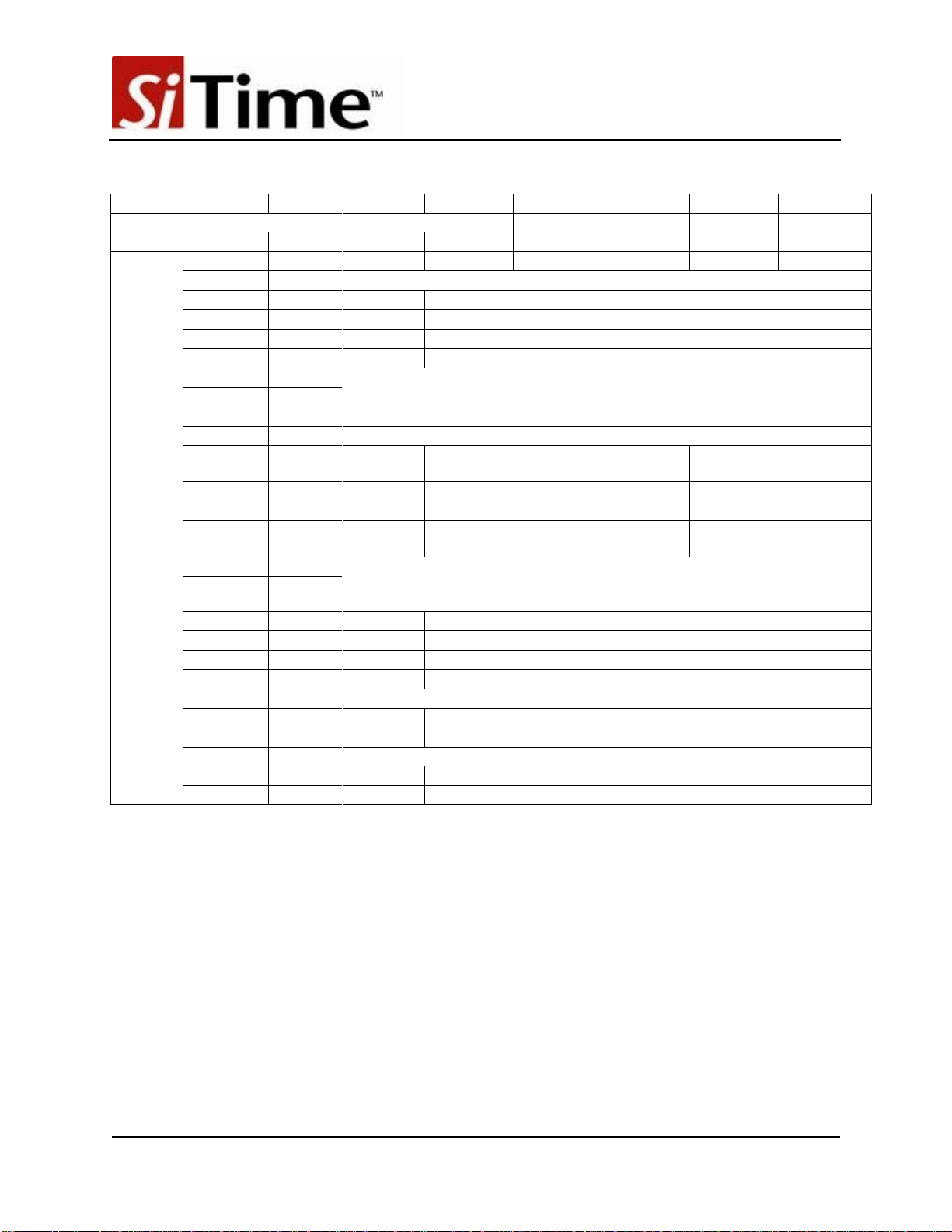
10 Appendix A: Programming the EnergyMicro EFM32 LFXO
10.1 EFM32 Clock Management Unit
All on-chip oscillators are controlled by a Clock Management Unit (CMU). The CMU provides
the capability to configure and turn on/off the clock on an individual basis to all peripheral
modules. It is possible to connect an external clock source to LFXTAL_N pin of the LFXO.
By configuring the LFXOMODE field in CMU_CTRL[12:11], the LFXO can be bypassed.
Table 9: CMU_CTRL - CMU Control Register
Offset
Bit Position
0x02C
31
30
29
28
27
26
25
24
23
22
21
20
19
18
17
16
15
14
13
12
11
10
9
8
7
6
5
4
3
2
1
0
Reset
0
0x0
0x3
0
1
0x0
0x3
0
0x1
0x3
0x0
Access
RW
RW
RW
RW
RW
RW
RW
RW
RW
RW
RW
Name
CLKOUTSEL1
CLKOUTSEL0
LFXOTMEOUT
LFXOBUFCUR
LFXOBOOST
LFXOMODE
HFXOTMEOUT
HFXOGLITCHDETEN
HFXOBUFCUR
HFXOBOOST
HFXOMODE
Table 10: The LFXOMODE Field
Value
Mode
Description
0
XTAL
32.768 kHz crystal oscillator
1
BUFEXTCLK
An AC coupled buffer is coupled in series with LFXTAL_N pin, suitable for external sinus
wave (32.768 kHz)
2
DIGEXTCLK
Digital external clock on LFXTAL_N pin. Oscillator is effectively bypassed.
To bypass the on-chip oscillator write '0x2' to the LFXOMODE[12:11] field.
The oscillator setting takes effect when 1 is written to LFXOEN in CMU_OSCENCMD.
The oscillator setting is reset to default when 1 is written to LFXODIS in CMU_OSCENCMD.
The Smart Timing Choice™ 10 SiT-AN10037 Rev 1.3
SiT15xx Optimized Drive Settings
Table 11: CMU_OSCENCMD - Oscillator Enable/Disable Command Register
Offset
Bit Position
0x02C
31
30
29
28
27
26
25
24
23
22
21
20
19
18
17
16
15
14
13
12
11
10
9
8
7
6
5
4
3
2
1
0
Reset
0
0
0
0
0
0
0
0
1
1
Access
W1
W1
W1
W1
W1
W1
W1
W1
W1
W1
Name
LFXODIS
LFXOEN
LFRCODIS
LFRCOEN
AUXHFRCO
DIS
AUXHFRCO
EN
HFXODIS
HFXOEN
HFRCODIS
HFRCOEN
Table 12: OSCENCMD - The [31:3] Field Descriptions
Bit
Name
Reset
Access
Description
31:10
Reserved
To ensure compatibility with future devices,
always write bits to 0.
9
LFXODIS
Disables the LFXO. LFXOEN has higher priority if written
simultaneously.
0
W1
LFXO Disable
8
LFXOEN
Enables the LFXO.
0
W1
LFXO Enable
7
LFRCODIS
Disables the LFRCO. LFRCOEN has higher priority if
written simultaneously.
0
W1
LFRCO Disable
6
LFRCOEN
Enables the LFRCO.
0
W1
LFRCO Enable
5
AUXHFRCODIS
Disables the AUXHFRCO. AUXHFRCOEN has higher
priority if written simultaneously. Warning: Do not disable
this clock during a flash erase/write operation.
0
W1
AUXHFRCO
Disable
4
AUXHFRCOEN
Enables the AUXHFRCO.
0
W1
AUXHFRCO
Enable
3
HFXODIS
Disables the HFXO. HFXOEN has higher priority if written
simultaneously. Do not disable the HFRXO if this
oscillator is selected as the source for HFCLK.
0
W1
HFXO Disable
The Smart Timing Choice™ 11 SiT-AN10037 Rev 1.3
SiT15xx Optimized Drive Settings
Table 13: CMU_STATUS - Status Register
Offset
Bit Position
0x02C
31
30
29
28
27
26
25
24
23
22
21
20
19
18
17
16
15
14
13
12
11
10
9
8
7
6
5
4
3
2
1
0
Reset
0
0
0
0
0
0
0
0
0
0
0
0
0
1
1
Access
R
R
R
R
R
R
R
R
R
R
R
R
R
R
R
Name
CALBSY
LFXOSEL
LFRCOSEL
HFXOSEL
HFRCOSEL
LFXORDY
LFXOENS
LFRCORDY
LFRCOENS
AUXHFRCO
RDY
AUXHFRCO
ENS
HFXORDY
HFXOENS
HFRCORDY
HFRCOENS
Table 14: CMU_STATUS - The [14:8] Field Descriptions
Bit
Name
Reset
Access
Description
31:15
Reserved
To ensure compatibility with future devices, always write
bits to 0.
14
CALBSY
Calibration is on-going
0
R
Calibration Busy
13
LFXOSEL
LFXO is selected as HFCLK clock source
0
R
LFXO Selected
12
LFRCOSEL
LFRCO is selected as HFCLK clock source
0
R
LFRCO Selected
11
HFXOSEL
HFXO is selected as HFCLK clock source
0
R
HFXO Selected
10
HFRCOSEL
HFRCO is selected as HFCLK clock source
1
R
HFRCO Selected
9
LFXORDY
LFXO is enabled and start-up time has
exceeded
0
R
LFXO Ready
8
LFXOENS
LFXO is enabled
0
R
LFXO Enable
Status

The Smart Timing Choice™ 12 SiT-AN10037 Rev 1.3
SiT15xx Optimized Drive Settings
10.2 Configuring the LFXO
Below is a code snippet of LFXO configuration from IAR Embedded Workbench IDE:
1. Enable the LFXO oscillator by setting the LFXOEN bit in the CMU_OSCENCMD[8]
(Table 11)
2. Wait until the LFXORDY bit in the CMU_STATUS[9] (Table 13) is set. Applicable only for
the XTAL mode, otherwise skip this step.
______________________________________________________________________________
CMU->CTRL &= ~(0x3 << 11);
CMU->CTRL |= 0x00000000; // (XTAL)32768 Hz crystal oscillator
//CMU->CTRL |= 0x00000800; // (BUFEXTCLK)AC coupled
//CMU->CTRL |= 0x00001000; // (DIGEXTCLK)an external clock source
// Lock CMU_CTRL
CMU->OSCENCMD = (0x1UL << 8);
/* Wait for clock to stabilize if requested
!!!Applicable only for crystal oscillator configuration!!! */
if (wait)
{
while (!(CMU->STATUS & (0x1 << 9)));
}
______________________________________________________________________________
The LFXO is able to operate from external clock sources with small signal amplitude (100mV
and above). This mode (AC mode - BUFEXTCLK) can be set by configuring the LFXMODE field
in the CMU_CTRL[12:11] register (see Table 9).

The Smart Timing Choice™ 13 SiT-AN10037 Rev 1.3
SiT15xx Optimized Drive Settings
11 Appendix B: Programming the STMicroelectronics STM32
LSE Oscillator
11.1 Low-speed External Clock Oscillator
The low-speed external (LSE) crystal oscillator can be switched on/off by setting/clearing the
LSEON bit in the RCC_CSR[8] register.
Table 15: Control/Status Register (RCC_CSR)
31
30
29
28
27
26
25
24
LPWR
RSTF
WWDG
RSTF
IWDG
RSTF
SFT
RSTF
POR
RSTF
PIN
RSTF
OBLRSF
RMVF
rw
rw
rw
rw
rw
rw
rw
rw
23
22
21
20
19
18
17
16
RTC
RST
RTC
EN
Reserved
RTCSEL
[1:0]
rw
rw
rw
rw
15
14
13
12
11
10
9
8
Reserved
LSECS
SD
LSECS
SON
LSE
BYP
LSERDY
LSEON
r
rw
rw
r
rw
7
6
5
4
3
2
1
0
Reserved
LSI
RDY
LSION
r
rw
The LSERDY flag in the RCC_CSR[9] register indicates whether the LSE crystal is stable or
not. At startup the LSE crystal output clock signal is not released until this bit is set by hardware.
An interrupt can be generated if enabled in the RCC_CIR[8] (Table 16).
Table 16: Clock Interrupt Register (RCC_CIR)
31
30
29
28
27
26
25
24
Reserved
23
22
21
20
19
18
17
16
CSSC
LSECS
SC
MSI
RDYC
PLL
RDYC
HSE
RDYC
HSI
RDYC
LSE
RDYC
LSI
RDYC
W
w
w
w
w
w
w
w
15
14
13
12
11
10
9
8
Res
LSECS
SIE
MSI
RDYIE
PLL
RDYIE
HSE
RDYIE
HSI
RDYIE
LSE
RDYIE
LSI
RDYIE
rw
rw
rw
rw
rw
rw
rw

The Smart Timing Choice™ 14 SiT-AN10037 Rev 1.3
SiT15xx Optimized Drive Settings
7
6
5
4
3
2
1
0
CSSF
LSE
RDYF
MSI
RDYF
PLL
RDYF
HSE
RDYF
HSI
RDYF
LSE
RDYF
LSI
RDYF
r
r
r
r
r
r
r
r
11.2 External Clock Source (LSE bypass)
It is possible to connect an external clock source to OSC32_IN pin of the LSE oscillator. This
feature is selected by setting the LSEBYP and LSEON bits in the RCC_CSR (Table 15). The
external clock signal (square, sine or triangle) with ~50% duty cycle has to drive the OSC32_IN
pin while the OSC32_OUT pin should be left unconnected (Hi-Z).
11.3 Clock Security System on LSE
The clock security system on the LSE oscillator can be activated by software writing the
LSECSSON in the RCC_CSR register (Table 15). This bit can be disabled only by a hardware
reset or RTC software reset, or after a failure detection on the LSE oscillator. LSECSSON must
be written after LSE and LSI are enabled (LSEON and LSION enabled) and ready (LSERDY
and LSIRDY set by hardware), and after the RTC clock has been selected by RTCSEL. The
CSS on LSE is working in all modes: Run, Sleep, Stop and Standby.
If a failure is detected on the external 32 kHz oscillator, the LSE clock is no longer supplied to
the RTC but no hardware action is made to the registers. In Standby mode a wakeup is
generated. In other modes an interrupt can be sent to wake up. The software MUST then
disable the LSECSSON bit, stop the defective 32 kHz oscillator (disabling LSEON), and can
change the RTC clock source (no clock or LSI or HSE, with RTCSEL), or take any required
action to secure the application.
11.4 Clock-out Capability
The microcontroller clock output (MCO) capability allows the clock to be output onto the external
MCO pin (PA8) using a configurable prescaler (1, 2, 4, 8, or 16). The configuration registers of
the corresponding GPIO port must be programmed in alternate function mode.
One of seven clock signals can be selected as the MCO clock:
System clock (SYSCLK)
Internal RC 16MHz (HSI) oscillator
Internal 65 kHz to 4.2 MHz (MSI) oscillator
External 1 to 24 MHz (HSE) oscillator
PLL
Internal low-power oscillator (LSI)
Low-power 32.768 kHz external oscillator (LSE)
The selection is controlled by the MCOSEL[2:0] bits of the RCC_CFGR register (Table 17).

The Smart Timing Choice™ 15 SiT-AN10037 Rev 1.3
SiT15xx Optimized Drive Settings
Table 17: Configuration Register (RCC_CFGR)
31
30
29
28
27
26
25
24
Res.
MCOPRE[2:0]
Res.
MCOSEL[2:0]
rw
rw
rw
rw
rw
rw
15
14
13
12
11
10
9
8
Reserved
PPRE2[2:0]
PPRE1[2:0]
rw
rw
rw
rw
rw
rw
23
22
21
20
19
18
17
16
PLLDIV[1:0]
PLLMUL[3:0]
Res.
PLL
SRC
rw
rw
rw
rw
rw
rw
rw
15
14
13
12
11
10
9
8
Reserved
PPRE2[2:0]
PPRE1[2:0]
rw
rw
rw
rw
rw
rw
7
6
5
4
3
2
1
0
HPRE1[3:0]
SWS[1:0]
SW[1:0]
rw
rw
rw
rw
rw
rw
rw
rw
Note: If the LSE or LSI is used as RTC clock source, the RTC continues to work in Stop and
Standby low power modes, and can be used as wake-up source. However, when the HSE clock
is used as RTC clock source, the RTC cannot be used in Stop and Standby low power modes.
11.5 Configuring LSE
1) Reset LSEON[8] and LSEBYP[10] bits in RCC_CSR before configuring the LSE.
IAR Embedded Workbench IDE example:
// #define RCC_LSE_OFF ((uint8_t)0x00)
/* Reset LSEON and LSEBYP bits before configuring the LSE --------*/
*(__IO uint8_t *) CSR_BYTE2_ADDRESS = RCC_LSE_OFF;
2) Set the new LSE configuration. Set LSEBYP[10] bit if you need the bypass mode and set the
LSEON bit. It can be performed simultaneously.
IAR Embedded Workbench IDE example:
// #define RCC_LSE_Bypass ((uint8_t)0x05)
// #define RCC_LSE_ON ((uint8_t)0x01)
/* Set the new LSE configuration ----------------------------------*/
*(__IO uint8_t *) CSR_BYTE2_ADDRESS = RCC_LSE_ON;
// or *(__IO uint8_t *) CSR_BYTE2_ADDRESS = RCC_LSE_Bypass;
3) Wait till the LSERDY[9] bit in RCC_CSR is ready. This is applicable when using an external
crystal.
The Smart Timing Choice™ 16 SiT-AN10037 Rev 1.3
SiT15xx Optimized Drive Settings
12 Appendix C: Programming the Renesas Electronics
RL78G13 XT1 Oscillator
12.1 XT1 Oscillator
The XT1 oscillator is a circuit with low gain in order to achieve low-power consumption. There
are AMPHS1[2], AMPHS0[1] fields in the CMC register (Table 20) that enables to choose
optimal gain for a crystal.
Table 18: Oscillation Mode Fields
AMPHS1
AMPHS0
XT1 oscillator oscillation mode selection
0
0
Low power consumption oscillation (default)
0
1
Normal oscillation
1
0
Ultra-low power consumption oscillation
1
1
Setting prohibited
12.2 Configuration XT1
1) Set the XTSTOP bit in CSC[6] to disable the XT1 oscillator.
2) Change the oscillation mode (AMPHS1, AMPHS0) if required.
3) Set the oscillator mode by setting/clearing EXCLKS, OSCSELS fields in the CMC
register (Table 20).
4) Clear the XTSTOP bit in CSC[6] (Table 19) to enable the XT1 oscillator.
Table 19: CSC Register
Symbol
<7>
<6>
5
4
3
2
1
<0>
CSC
MSTOP
XTSTOP
0
0
0
0
0
HIOSTOP
MSTOP
High-speed system clock operation control
X1 oscillation mode
External clock input mode
Input port mode
0
X1 oscillator operating
External clock from EXCLK pin is valid
Input port
1
X1 oscillator stopped
External clock from EXCLK pin is invalid
XTSTOP
Subsystem clock operation control
XT1 oscillation mode
External clock input mode
0
XT1 oscillator operating
External clock from EXCLKS pin is valid
Input port
1
XT1 oscillator stopped
External clock from EXCLKS pin is
invalid
HIOSTOP
High-speed on-chip oscillator clock operation control
0
High-speed on-chip oscillator operating
1
High-speed on-chip oscillator stopped

The Smart Timing Choice™ 17 SiT-AN10037 Rev 1.3
SiT15xx Optimized Drive Settings
Table 20: CMC Register
Symbol
7
6
5
4
3
2
1
0
CMC
EXCLK
OSCSEL
EXCLKS
OSCSELS
0
AMPHS1
AMPHS0
AMPH
EXCLK
OSCSEL
High-speed system clock pin
operation mode
X1/P121 pin
X2/EXCLK/P122 pin
0
0
Input port mode
Input port
0
1
X1 oscillation mode
Crystal/ceramic resonator connection
1
0
Input port mode
Input port
1
1
External clock input mode
Input port
External clock input
EXCLKS
OSCSELS
Subsystem clock pin
operation mode
XT1/P123 pin
XT2/EXCLKS/P124 pin
0
0
Input port
0
1
Crystal resonator connection
1
0
Input port
1
1
Input port
External clock input
AMPHS1
AMPHS0
XT1 oscillator oscillation mode selection
0
0
Low power consumption oscillation (default)
0
1
Normal oscillation
1
0
Ultra-low power consumption oscillation
1
1
Setting prohibited
AMPH
Control of X1 clock oscillation frequency
0
1 MHz ≤ fx ≤ 10 MHz
1
10 MHz ≤ fx ≤ 20 MHz
The Smart Timing Choice™ 18 SiT-AN10037 Rev 1.3
SiT15xx Optimized Drive Settings
13 Appendix D: Programming the Texas Instruments MSP430
low frequency oscillator
13.1 The MSP430 LFXT Oscillator
The LFXT1 oscillator supports ultra-low current consumption using a 32768 Hz watch crystal in
LF mode (XTS = 0) or a high frequency crystal in HF mode. A watch crystal connects with the
XIN and XOUT pins without any other external components. The software-selectable XCAPx
bits configure the internally provided load capacitance for the LFXT1 crystal in LF mode. This
capacitance can be selected as 1 pF, 6 pF, 10 pF, or 12.5 pF typical. Additional external
capacitors can be added if necessary. The LFXT1 oscillator is not implemented in the
MSP430G22x0 device family.
The LFXT1 oscillator also supports high-speed crystals or resonators when in HF mode (XTS =
1, XCAPx = 00). The high-speed crystal or resonator connects to XIN and XOUT and requires
external capacitors on both terminals. When LFXT1 is in HF mode, the LFXT1Sx bits select the
range of operation. LFXT1 may be used with an external clock signal on the XIN pin in either LF
or HF mode when LFXT1Sx = 11, OSCOFF = 0, and XCAPx = 00. When used with an external
signal, the external frequency must meet the data sheet parameters for the chosen mode. When
the input frequency is below the specified lower limit, the LFXT1OF bit may be set preventing
the CPU from being clocked with LFXT1CLK.
Steps to configure the LFXT1 oscillator:
1) Set the mode in XTS and the divider value in DIVAx.
2) Choose mode by changing the LFXT1Sx bits in BCSCTL3.
3) Enable internal capacitors if needed. It is controlled by XCAPx in BCSCTL3.
4) Turn on the oscillator by clearing XT2OFF in BCSCTL1.
Table 21: BCSCTL1, Basic Clock System Control Register 1
Bit
7
6
5
4
3
2
1
0
Name
XT2OFF
XTS
DIVAx
RSELx
State
rw-(1)
rw-(0)
rw-(0)
rw-(0)
rw-0
rw-1
rw-1
rw-1
XT2OFF
Bit 7
XT2 off. This bit turns off the XT2 oscillator
0 XT2 is on
1 XT2 if off
XTS
Bit 6
LFXT1 mode select
0 Low-frequency mode
1 High-frequency mode
DIVAx
Bits 5-4
Divider for ACLK
00 /1
01 /2
10 /4
11 /8
RSELx
Bits 3-0
Range select. Sixteen different frequency ranges are
available. The lowest frequency range is selected by setting
RSELx = 0. RSEL3 is ignored when DCOR = 1
The Smart Timing Choice™ 19 SiT-AN10037 Rev 1.3
SiT15xx Optimized Drive Settings
Table 22: BCSCTL3, Basic Clock System Control Register 3
Bit
7
6
5
4
3
2
1
0
Name
XT2Sx
LFXT1Sx
XCAPx
XT2OF
LFXT1OF
State
rw-0
rw-0
rw-0
rw-0
rw-0
rw-1
r0
r-(1)
XT2Sx
Bits 7-6
XT2 range select. These bits select the frequency range for XT2.
00
0.4- to 1-MHz crystal or resonator
01
1- to 3-MHz crystal or resonator
10
3- to 16-MHz crystal or resonator
11
Digital external 0.4- to 16-MHz clock source
LFXT1Sx
Bits 5-4
Low-frequency clock select and LFXT1 range select. These bits select
between LFXT1 and VLO when XTS = 0, and select the frequency range
for LFXT1 when XTS = 1.
When XTS = 0:
When XTS = 1:
00
32768-Hz crystal on
LFXT1
00
0.4- to 1-MHz crystal
01
Reserved
01
1- to 3-MHz crystal
10
VLOCLK
10
3- to 16-MHz crystal
11
External clock source
11
0.4- to 16-MHz clock
source
XCAPx
Bits 3-2
Oscillator capacitor selection. These bits select the effective capacitance
seen by the LFXT1 crystal when XTS = 0. If XTS = 1 or if LFXT1Sx = 11
XCAPx should be 00.
00
~1 pF
01
~6 pF
10
~10 pF
11
~12.5 pF
XT2OF
Bit 1
XT2 oscillator fault
0
No fault condition present
1
Fault condition present
LFXT1OF
Bit 0
LFXT1 oscillator fault
0
No fault condition present
1
Fault condition present
Below is the configuration code of base clock module example from IAR Embedded Workbench
IDE:
BCSCTL3 = 0x00; // 32768-Hz crystal, 1pF internal capacitor
BCSCTL1 = 0x00; // XT2 oscillator is on, Low-frequency mode
The Smart Timing Choice™ 20 SiT-AN10037 Rev 1.3
SiT15xx Optimized Drive Settings
13.2 Clock-out Capability
The microcontroller can be easily configured to clock external on-board peripherals from one of
its pins. For this you need configure the PxSEL and PxSEL2 function registers that are used to
select the pin function. A pin has to be configured as an output by setting needed in PxDIR.
Below is code from IAR Embedded Workbench that configures it:
P2SEL = P2SEL | 0x01; // Select ACLK function for pin
P2DIR = P2DIR | 0x01; // Set direction of P2.0 to output
Table 23: PxSEL and PxSEL2
PxSEL2
PxSEL
Pin Function
0
0
I/O function is selected
0
1
Primary peripheral module function is selected
1
0
Reserved. See device-specific data sheet
1
1
Secondary peripheral module function is selected
13.3 Low-power Modes
The MSP430 devices have several low-power modes. Every LPMx low-power mode allows
developers to create an application with balanced power consumption. The low-power modes
are configured with the CPUOFF, OSCOFF, SCG0, and SCG1 bits in the status register. The
advantage of including the CPUOFF, OSCOFF, SCG0, and SCG1 mode-control bits in the
status register is that the present operating mode is saved onto the stack during an interrupt
service routine.
The ACLK clock is working in LPM0-LPM3 modes. The LPM4 mode disables CPU and all
clocks.
Table 24: Status Register
15
14
13
12
11
10
9
8
7
6
5
4
3
2
1
0
Reserved
V
SCG1
SCG0
OSCOFF
CPUOFF
GIE
N
Z
C
Table 25: Low Power Modes and ACLK Clock
SCG1
SCG0
OSCOFF
CPUOFF
Mode
ACLK
0
0
0
0
Active
Enabled
0
0
0
1
LPM0
Enabled
0
1
0
1
LPM1
Enabled
1
0
0
1
LPM2
Enabled
1
1
0
1
LPM3
Enabled
1
1
1
1
LPM4
Disabled
Table of contents


