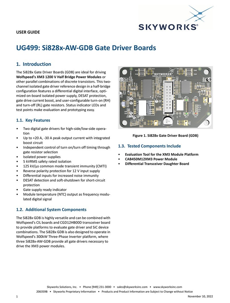
Skyworks Si5361 User manual

Si5361/62/63 Reference Manual
Any-frequency, Any-output Jitter-Attenuators/Clock Multipliers
Si5361/62/63 Family Reference Manual
This Family Reference Manual is intended to provide hardware, system, and software
engineers the necessary technical information to successfully use the Si5361/62/63
in end applications. The official device specifications and ordering information can be
found in the Si5361/62/63 data sheets.
The Si5361/62/63 jitter attenuating clock multipliers combine fifth-generation DSPLL and
MultiSynth™ technologies to enable any-frequency clock generation. These parts are
used for applications that require the highest level of jitter performance. The Si5361,
Si5362, and Si5363 are 1-, 2-, and 3-DSPLL devices, respectively. These devices are
programmable with a serial interface. Alternatively, on-chip, programmable, non-volatile
memory (NVM) can be used to ensure powerup with known frequency configurations.
Free-run, synchronous, and holdover modes of operation are supported offering both
automatic and manual input clock switching. The loop filter is fully integrated on-chip
eliminating the risk of potential noise coupling associated with discrete solutions. Fur-
ther, the jitter attenuation bandwidth is digitally programmable providing jitter perform-
ance optimization at the application level. These devices are capable of generating any
combination of output frequencies from any input frequency within the specified input
and output range.
The Si5361/62/63 is programmed using Skyworks ClockBuilder software and can be
made to power up with known frequencies as a factory programmed custom part, or can
be ordered as a "custom blank" part for increased flexibility.
RELATED DOCUMENTS
• Si5361/62/63 Data Sheet
• UG514: Si536x-EVB User's Guide
• Si55xx, Si540x, and Si536x
Recommended XTAL, XO, VCXO, TCXO,
and OCXO Reference Manual
• AN1357: Si5360/61/62/63 Schematic
Design and Board Layout Guidelines
• AN1360: Serial Communications and
API Programming Guide for Si536x,
Si540x,and Si55xx Devices
Skyworks Solutions, Inc. • Phone [781] 376-3000 • Fax [781] 376-3100 • [email protected] • www.skyworksinc.com
1206420A • Skyworks Proprietary Information • Products and Product Information are Subject to Change Without Notice • November 7, 2022 1

Table of Contents
1. Introduction to the Si5361/62/63 and ClockBuilder Pro ...............5
2. Use Cases with the Si5361/62/63 Jitter Attenuator Applications ............6
2.1 Si5361 Application Example .........................6
2.2 Si5362/63 Application Examples ........................7
2.3 Si5363 Application Example .........................9
3. DSPLL and MultiSynth ........................... 10
3.1 Dividers ................................13
3.2 DSPLL Loop Bandwidth ...........................13
3.3 Output Skew Control ............................13
3.3.1 VCO Frequency Range .........................13
4. Modes of Operation ............................ 14
4.1 Reset and Initialization ...........................14
4.2 Free-Run Mode .............................14
4.3 Lock Acquisition Mode ...........................15
4.4 Locked Mode ..............................15
4.5 Holdover Mode ..............................15
5. Dynamic Frequency Changes ........................ 16
5.1 Digitally-Controlled Oscillator (DCO).......................16
5.2 Frequency-On-The-Fly ...........................16
6. Zero Delay Mode (ZDM) .......................... 17
7. Reference Inputs ............................. 18
7.1 Crystal (XTAL) Reference ..........................18
7.2 Crystal Oscillator (XO) Reference .......................18
8. Input Clocks............................... 19
8.1 Differential Inputs .............................19
8.2 CMOS and Dual CMOS Inputs ........................19
8.3 Unused Inputs ..............................19
8.4 Phase Readout (PHRD) ..........................19
8.5 Input Clock Selection ...........................19
8.5.1 Manual Input Clock Select ........................19
8.5.2 Automatic Input Selection .........................20
8.6 Smart Input Switching ...........................20
8.6.1 Switching between Non-0 ppm Offset .....................20
8.6.2 Switching between 0 ppm Offset ......................20
9. Output Clocks .............................. 22
Skyworks Solutions, Inc. • Phone [781] 376-3000 • Fax [781] 376-3100 • [email protected] • www.skyworksinc.com
2206420A • Skyworks Proprietary Information • Products and Product Information are Subject to Change Without Notice • November 7, 2022 2

9.1 Output Crosspoint Switch ..........................22
9.2 Output Signal Format and Terminations .....................22
9.2.1 Differential Outputs ...........................23
9.2.2 LVCMOS Output Terminations .......................23
9.2.3 Slew Rate Limited (SRL) CMOS Outputs ...................23
9.2.4 LVCMOS and SRL CMOS Output Settings ...................23
9.3 Output Enable/Disable ...........................24
9.4 State of Disabled Output ..........................25
10. Status and Alarms ............................ 26
10.1 Status Monitoring ............................27
10.2 Input Clock Status ............................27
10.2.1 Loss of Signal (LOS) ..........................28
10.2.2 Out of Frequency (OOF) ........................29
10.2.3 Phase Monitor (PHMON) ........................30
10.2.4 Short Term Holdover ..........................31
10.3 PLL Status ..............................31
10.3.1 Frequency Loss of Lock (FLOL) ......................32
10.3.2 Status Bits .............................32
10.3.3 Phase Loss of Lock (PLOL) .......................33
10.3.4 Cycle Slip Detection ..........................33
10.3.5 External Reference Status ........................34
10.3.6 Interrupt Status ............................34
11. GPIO (General Purpose Input/Output) ..................... 35
11.1 GPIO General Settings ..........................35
11.2 Unused Outputs as GPIs ..........................35
11.3 GPIO Pin Function Descriptions ........................36
11.4 Reset Pin (RSTb) ............................36
12. Serial Interface ............................. 37
12.1 SPI Interface ..............................37
12.2 I2C Interface ..............................40
13. Power Supplies & Voltage Detection ..................... 43
13.1 VDDA Primacy .............................43
13.2 Power Supply Sequencing .........................43
13.3 Power Supply Ramp Rate .........................43
13.4 Power Supply Bypassing and Filtering Recommendations ...............43
13.5 Voltage Detection ............................43
13.6 Power Management Features ........................43
13.7 Low Power Mode.............................43
14. Custom Programmed Parts vs. Custom Blank Parts ............... 44
14.1 Custom Programmed Parts .........................44
Skyworks Solutions, Inc. • Phone [781] 376-3000 • Fax [781] 376-3100 • [email protected] • www.skyworksinc.com
3206420A • Skyworks Proprietary Information • Products and Product Information are Subject to Change Without Notice • November 7, 2022 3

14.2 Custom Blank Parts ............................44
15. Work Flow Using ClockBuilderTM Pro (CBProTM) and the Application Programming
Interface (Device API)........................... 45
15.1 Field Programming ............................45
16. Application Programming Interface (Device API) ................ 46
17. Revision History............................. 47
Skyworks Solutions, Inc. • Phone [781] 376-3000 • Fax [781] 376-3100 • [email protected] • www.skyworksinc.com
4206420A • Skyworks Proprietary Information • Products and Product Information are Subject to Change Without Notice • November 7, 2022 4

1. Introduction to the Si5361/62/63 and ClockBuilder Pro
The Si5361/62/63 family are jitter attenuator devices that support flexible frequency planning with up to three clock domains. This
device family is designed to support synchronization in line card solutions for network applications like Synchronous Ethernet, SONET,
SDH, OTN. Other applications include:
• 56G/112G/224G PAM4 SerDes clocking
• GbE / 10 GbE / 100G SyncE
• OTN muxponders and transponders
• Medical imaging
• Test and measurement
ClockBuilder Pro software is used to create a frequency plan and a custom programmed or custom blank orderable part number (OPN)
for the Si5361/62/63 jitter attenuator. During operation, the Device API embedded on the clock devices may be used to dynamically
adjust or poll the Si5361/62/63 parameters. To learn more about configuration settings of the Si5361/62/63, open a ClockBuilder Pro
Sample Plan and explore.
Figure 1.1. ClockBuilder Pro Front Wizard Front Panel showing Sample Plans
This family reference manual provides information on the Si5361/62/63 hardware capabilities. ClockBuilder Pro and the Device API are
discussed further at the end of this document. The full documentation for the Device API depends on the part number and is available
by link from ClockBuilder Pro.
Si5361/62/63 Reference Manual • Introduction to the Si5361/62/63 and ClockBuilder Pro
Skyworks Solutions, Inc. • Phone [781] 376-3000 • Fax [781] 376-3100 • [email protected] • www.skyworksinc.com
5206420A • Skyworks Proprietary Information • Products and Product Information are Subject to Change Without Notice • November 7, 2022 5

2. Use Cases with the Si5361/62/63 Jitter Attenuator Applications
This section will describe many of the intended use cases and end applications for the Si5361/61/63 family of devices.
2.1 Si5361 Application Example
Typical applications of the Si5361 device include
1. 10/40/100/200/400G networking line cards
2. SONET/SHD line cards
3. Jitter cleaner
The image below shows the Si5361 used in a typical SyncE architecture as a line card device. It also shows Skywork's Si540x
device acting as a timing card to distribute timing information from different Building Integrated Timing Supplies (BITS).
LAN / WAN
SyncE Line Card
Si5361
112/224 GbE
PHY
112/224 GbE
PHY
Hitless Switching
Jitter Filtering
Frequency Translation
8 kHz
19.44 MHz
25 MHz
DSPLL P
Rx Timing Path
Tx Timing Path
Line Recovered
Clocks
Si5348
Wander Filtering
Hitless Switching
Holdover
Redundant
Timing Cards
TCXO/
OCXO
BITS A
8 kHz
19.44 MHz
25 MHz
A
B
LAN / WAN
SyncE Line Card
A
B
Si5361
112/224 GbE
PHY
Hitless Switching
Jitter Filtering
Frequency Translation
8 kHz
19.44 MHz
25 MHz
DSPLL P
Rx Timing Path
Tx Timing Path
Line Recovered
Clocks
A
B
Line Recovered Timing
Telecom or
Ethernet
Backplane
156.25 MHz
155.52 MHz
161.1328125 MHz
156.25 MHz
155.52 MHz
161.1328125 MHz
Si540x
BITS B
112/224 GbE
PHY
Figure 2.1. Si5361 as Line Card Device
Si5361/62/63 Reference Manual • Use Cases with the Si5361/62/63 Jitter Attenuator Applications
Skyworks Solutions, Inc. • Phone [781] 376-3000 • Fax [781] 376-3100 • [email protected] • www.skyworksinc.com
6206420A • Skyworks Proprietary Information • Products and Product Information are Subject to Change Without Notice • November 7, 2022 6

2.2 Si5362/63 Application Examples
The application schematic in the figure below shows the Si5362/63 devices used in SyncE line cards. These multi-PLL devices provide
independent timing paths to generate ultra low jitter PHY layer clock frequencies and at the same time clean up the recovered PHY
clocks and generate output clock frequencies that connect to the Ethernet backplane.
LAN / WAN
SyncE Line Card
Si5362/63
Hitless Switching
Jitter Filtering
Frequency Translation
DSPLL P
DSPLL A/B
Rx Timing Path
Tx Timing Path
Line Recovered
Clocks
112/224 GbE
PHY
112/224 GbE
PHY
8 kHz
19.44 MHz
25 MHz
156.25 MHz
155.52 MHz
161.1328125 MHz
Si5348
Wander Filtering
Hitless Switching
Holdover
Redundant
Timing Cards
TCXO/
OCXO
BITS A
BITS B
8 kHz
19.44 MHz
25 MHz
A
B
LAN / WAN
SyncE Line Card
A
B
Si5362/63
Hitless Switching
Jitter Filtering
Frequency Translation
DSPLL P
DSPLL A/B
Rx Timing Path
Tx Timing Path
Line Recovered
Clocks
A
B
Line Recovered Timing
Telecom or
Ethernet
Backplane
112/224 GbE
PHY
8 kHz
19.44 MHz
25 MHz
156.25 MHz
155.52 MHz
161.1328125 MHz
Si540x
112/224 GbE
PHY
Figure 2.2. Si5362/63 as SyncE Line Card
Si5361/62/63 Reference Manual • Use Cases with the Si5361/62/63 Jitter Attenuator Applications
Skyworks Solutions, Inc. • Phone [781] 376-3000 • Fax [781] 376-3100 • [email protected] • www.skyworksinc.com
7206420A • Skyworks Proprietary Information • Products and Product Information are Subject to Change Without Notice • November 7, 2022 7

Si5362/63 devices can be deployed in IEEE 1588 Precision Time Protocol line card applications as shown in Fig 2.3 below. The
reference PLL (DSPLLP) receives the SyncE clocks from the Network Synchronizers such as Skyworks' Si540x family devices. Note
that Network Synchronizer devices allow to support Sysclk to drive the ToD counter. These SyncE input clocks are now used to
generate ultra low jitter Ethernet PHY layer clock output frequencies. DSPLLP provides jitter filtering for noise picked up over the
backplane. The DSPLLA (for Si5362) and DSPLLA/B (for Si5363) can be used as an independent timing path to generate System clock
for the 1588 Time of Day (ToD) counter. The main advantage of this scheme is any changes to DSPLLA/B made to adjust the ToD
counter will not affect the PHY layer.
PHY
FPGA
Si5362/63
DSPLL A/B
ToD
Host
PHY
DSPLL P
n
Timestamps
Si540x
DSPLL B
DSPLL A
Line Card
Host
DCO
Timing Card Primary
Timing Card Secondary
SyncE (primary)
SyncE (secondary)
Sysclk
SyncE
SyncE
Tx PHY’sRx PHY’s
Sysclk
Backplane
DCO Ctrl
DCO Ctrl
Figure 2.3. Si5362/63 in 1588 Application
Note: When multiple inputs are assigned to DSPLLP, switching between them will affect all device outputs.
Si5361/62/63 Reference Manual • Use Cases with the Si5361/62/63 Jitter Attenuator Applications
Skyworks Solutions, Inc. • Phone [781] 376-3000 • Fax [781] 376-3100 • [email protected] • www.skyworksinc.com
8206420A • Skyworks Proprietary Information • Products and Product Information are Subject to Change Without Notice • November 7, 2022 8

2.3 Si5363 Application Example
This section describes another popular application for the multi-PLL Si5363 device. Muxponders used in OTN (Optical Transport
Network) protocol helps reduce the number of wavelengths required to transmit the data by aggregating multiple services into single
wavelength. This allows to maximize the fiber capacity and thus increase network efficiency. The three independent timing paths
(DSPLL P, DSPLL A and DSPLL B) provided by Si5363 device are used to clean up the gapped clock in an OTN Muxponder
Si5363
DSPLL P
DSPLL A
DSPLL B
Data
Clock
Client #3
High Jitter Clock
PHY
Jitter Attenuated
Non-Gapped Clock
Data
Clock
Client #2
High Jitter Clock
PHY
Jitter Attenuated
Non-Gapped Clock
Data
Clock
Client #1
High Jitter Clock
PHY
Jitter Attenuated
Non-Gapped Clock
200-400G OTN
OTN Muxponder
OTN Demapper
112/224 GbE
112/224 GbE
112/224 GbE
Figure 2.4. Si5363 in OTN Muxponder Application
Note: When multiple inputs are assigned to DSPLLP, switching between them will affect all device outputs.
Si5361/62/63 Reference Manual • Use Cases with the Si5361/62/63 Jitter Attenuator Applications
Skyworks Solutions, Inc. • Phone [781] 376-3000 • Fax [781] 376-3100 • [email protected] • www.skyworksinc.com
9206420A • Skyworks Proprietary Information • Products and Product Information are Subject to Change Without Notice • November 7, 2022 9

3. DSPLL and MultiSynth
The DSPLL is responsible for input frequency translation and jitter attenuation. The input dividers (Pxn/Pxd) allow for integer or
fractional division of the input frequency. The DSPLL can perform hitless switching between input clocks (INx) if enabled. Input
switching is controlled manually or automatically using an internal state machine. The external reference (XTAL or XO) provides a
frequency reference which determines output frequency stability and accuracy while the device is in free-run or holdover mode. It is
also the jitter reference for the device. Note that either a XTAL on XA/XB or an XO on XO_IN is always required. The high-performance
MultiSynth dividers (NA/NB) generate fractionally related output frequencies for the output stage, while Q dividers generate integer
related output frequencies. A crosspoint switch connects any of the generated frequencies to any of the outputs. A single MultiSynth
output can connect to one or more output drivers. Additional integer division (R) determines the final output frequency.
For the Si5362/63 devices, each of the DSPLLs operate independently from each other and are controlled through a common serial
interface. Each DSPLL has access to any of the four inputs (IN0 to IN3) after having been divided down by the P dividers, which are
either fractional or integer. The block diagrams and functional operation are discussed in turn below.
The Si5361 is a single PLL device. The Si5361 has two MultiSynth available, NA and NB.
PD
VCO
DSPLL P x18
MP
DIV
÷P
÷P
IN2
÷P
÷P
IN1
÷P
IN0
÷P
IN3
Si5361
OUT1
÷R
OUT0
÷R
OUT3
÷R
OUT2
÷R
OUT17
÷R
OUT5
÷R
OUT4
÷R
OUT6
÷R
÷Q
NB
DIV
XTAL / XO
XO_IN
XO_INb
XA XB
OSC
XTAL
NA
DIV
Figure 3.1. Si5361 Detailed Block Diagram
Si5361/62/63 Reference Manual • DSPLL and MultiSynth
Skyworks Solutions, Inc. • Phone [781] 376-3000 • Fax [781] 376-3100 • [email protected] • www.skyworksinc.com
10 206420A • Skyworks Proprietary Information • Products and Product Information are Subject to Change Without Notice • November 7, 2022 10

The Si5362 is a 2 PLL device with one MultiSynth. The Si5362 can be programmed to drive the NB divider through either DSPLLP or
DSPLLA. When DSPLLA is not used, NA can also be driven through DSPLLP.
PD
VCO
DSPLL P x18
MP
DIV
÷P
÷P
IN2
÷P
÷P
IN1
÷P
IN0
÷P
IN3
Si5362
OUT1
÷R
OUT0
÷R
OUT3
÷R
OUT2
÷R
OUT17
÷R
OUT5
÷R
OUT4
÷R
OUT6
÷R
÷Q
DSPLL A
PD
MA
DIV
NA
DIV
NB
DIV
XTAL / XO
XO_IN
XO_INb
XA XB
OSC
XTAL
Figure 3.2. Si5362 Detailed Block Diagram
Si5361/62/63 Reference Manual • DSPLL and MultiSynth
Skyworks Solutions, Inc. • Phone [781] 376-3000 • Fax [781] 376-3100 • [email protected] • www.skyworksinc.com
11 206420A • Skyworks Proprietary Information • Products and Product Information are Subject to Change Without Notice • November 7, 2022 11

The Si5363 is a 3 PLL device. When DSPLLA and/or DSPLLB are not used, the Si5363 allows users to select single DSPLL operation
with or without NA/NB dividers driven through DSPLLP.
PD
VCO
DSPLL P x18
MP
DIV
÷P
÷P
IN2
÷P
÷P
IN1
÷P
IN0
÷P
IN3
Si5363
OUT1
÷R
OUT0
÷R
OUT3
÷R
OUT2
÷R
OUT17
÷R
OUT5
÷R
OUT4
÷R
OUT6
÷R
÷Q
DSPLL A
PD
MA
DIV
NA
DIV
DSPLL B
PD
MB
DIV
NB
DIV
XTAL / XO
XO_IN
XO_INb
XA XB
OSC
XTAL
Figure 3.3. Si5363 Detailed Block Diagram
Si5361/62/63 Reference Manual • DSPLL and MultiSynth
Skyworks Solutions, Inc. • Phone [781] 376-3000 • Fax [781] 376-3100 • [email protected] • www.skyworksinc.com
12 206420A • Skyworks Proprietary Information • Products and Product Information are Subject to Change Without Notice • November 7, 2022 12

3.1 Dividers
The Si5361/62/63 has both fractional and integer frequency dividers. The block diagrams in Figures 3.1 and 3.2 show the location of
each divider and how it fits into the signal flow for all the three devices. The ClockBuilder Pro software will choose the optimal divide
values based on the frequency plan the user wishes to create. A description of each type of divider is listed below:
1. Input P Divider: P3, P3b, P2, P2b, P1, P0
• Integer or Fractional Divide Value
• Minimum value is 1
2. DSPLL P Output Q Divider: Q17-Q0
• Integer Only Divide Value
• Open loop divider taps directly off VCO
3. DSPLLA/B Output NA, NB Divider
• MultiSynth Divider
• Fractional Divide Value
4. DSPLLA/B Feedback MA, MB Divider
• Fractional Divide Value
5. Output R Divider: R17-R0
• Integer Only Divide Value
• Minimum value is 2 if signal comes from NA/NB; Minimum value is 1 if signal comes from Q divider
3.2 DSPLL Loop Bandwidth
The DSPLL loop bandwidth determines the amount of input clock jitter attenuation. The DSPLL loop bandwidth is configurable within
the range of 20 Hz to 4 kHz. The loop bandwidth is controlled digitally and remains stable with less than 0.1 dB of peaking for any loop
bandwidth selected. The DSPLL loop bandwidth can be set using ClockBuilder Pro or from Device API commands during operation. In
general, increasing PLL bandwidth speeds up lock acquisition while decreasing jitter attenuation. For DSPLLP, using loop bandwidth
between 20 Hz to 40 Hz provides a good optimization for both jitter and wander performance.
Selecting a low DSPLL loop bandwidth will generally lengthen the lock acquisition time but also increase jitter attenuation. The Fastlock
feature allows setting a temporary Fastlock Loop Bandwidth that is used during the lock acquisition process to reduce lock time.
Higher Fastlock loop bandwidth settings will enable the DSPLLs to lock faster. Once lock acquisition has completed, the DSPLL’s loop
bandwidth will automatically revert to the nominal DSPLL Loop Bandwidth setting. The Fastlock feature can be enabled or disabled
independently using ClockBuilder Pro. If enabled, when LOL is asserted Fastlock will be automatically applied. When LOL is no longer
asserted, Fastlock will be automatically disabled. The loss of lock (LOL) feature is a fault monitoring mechanism. Details of the LOL
feature can be found in the fault monitoring section. For more information, please see "AN1365: Si5361/62/63 Lock Time Parameters".
3.3 Output Skew Control
Output skew control allows outputs that are derived from the Q dividers to be phase adjusted in steps of 1/fVCO, or 1/(4*fVCO) when
fine adjust is enabled. Output skew is programmable and the output delay adjustment range is displayed in ClockBuilder Pro.
In addition to output skew control, groupings of Q divider clock outputs can be adjusted with dynamic phase adjust. Dynamic phase
adjustment changes the phase of grouped clock outputs to be earlier or later. For more information the Device API documentation.
3.3.1 VCO Frequency Range
In the Si5361/62/63, the VCO frequency range is 10.4 GHz to 13.0 GHz. The output delay (skew) adjustment range will vary depending
on VCO frequency used in the plan. To find the specific fVCO used in a frequency plan, see the ClockBuilder Pro Design Report.
Si5361/62/63 Reference Manual • DSPLL and MultiSynth
Skyworks Solutions, Inc. • Phone [781] 376-3000 • Fax [781] 376-3100 • [email protected] • www.skyworksinc.com
13 206420A • Skyworks Proprietary Information • Products and Product Information are Subject to Change Without Notice • November 7, 2022 13

4. Modes of Operation
Once initialization is complete, each of the PLLs of the Si5361/62/63 operates independently in one of four modes: Free-run Mode,
Lock Acquisition Mode, Locked Mode, or Holdover Mode. A state diagram showing the modes of operation is shown in the figure below.
The following sections describe each of these modes in greater detail.
No valid
input clocks
selected
Lock Acquisition
Locked
Mode
Holdover
Mode
Phase lock on
selected input
clock is achieved
An input is
qualified and
available for
selection
No valid input
clocks available
for selection
Free-run
Valid input clock
selected
Reset and
Initialization
Power-Up
Selected input
clock fails
Yes
No
Holdover
History
Valid?
Other Valid
Clock Inputs
Available?
No
Yes
Input Clock
Switch
Figure 4.1. State Machine Modes of Operation
The above diagram shows the clock operating states such as reset, free-run, holdover and locked mode. These operating modes are
discussed briefly below and explained in more detail in later sections of this document.
4.1 Reset and Initialization
Once power is applied, the device begins an initialization period where it downloads default firmware and configuration data from
internal non-volatile memory (NVM) and performs other initialization tasks. Communicating with the device through the serial interface
is possible once this initialization period is complete. No clocks will be generated until the initialization is complete.
There are two types of resets available. A hard reset is functionally similar to a device power-up. All device settings will be restored to
the values stored in NVM, and all circuits will be restored to their initial state including the serial interface. A hard reset is initiated using
the RST pin. A soft reset bypasses the NVM download. Soft reset can be initiated using Device API commands in ClockBuilder Pro.
4.2 Free-Run Mode
The frequency accuracy of the generated output clocks is entirely dependent on the frequency accuracy of the reference clock source.
If a XTAL is connected to the XA/XB pins, then the clock outputs will generate a frequency at the XTAL’s accuracy. For example, if a
XTAL is operating at –28 ppm, then clock outputs will also be –28 ppm. The same is true if an XO is connected at the XO_IN/XO_INb
inputs instead of using XTAL at XA/XB.
ClockBuilder Pro provides an option to force DSPLL P, DSPLL A, and DSPLL B into free-run on power-up. When ready to lock the PLL,
the host must use the FORCE_HOLDOVER API command. The FORCE_HOLDOVER command in the Device API is used to force a
PLL into or out of holdover mode.
Si5361/62/63 Reference Manual • Modes of Operation
Skyworks Solutions, Inc. • Phone [781] 376-3000 • Fax [781] 376-3100 • [email protected] • www.skyworksinc.com
14 206420A • Skyworks Proprietary Information • Products and Product Information are Subject to Change Without Notice • November 7, 2022 14

4.3 Lock Acquisition Mode
The DSPLL independently monitors its configured inputs for a valid clock. If configured for automatic input selection, the PLL will
automatically start the lock acquisition process to the highest priority input clock, if any are available. If configured for manual input
selection, the PLL will automatically start the lock acquisition process if the currently selected input clock is available. If Fastlock
feature is enabled, they will acquire lock faster than the PLL Loop Bandwidth would provide and then transition to the normal PLL loop
bandwidth. During lock acquisition, the outputs will generate a clock that follows the VCO frequency change as it pulls-in to the input
clock frequency.
4.4 Locked Mode
Once locked, the PLL will generate clock outputs that are both frequency and phase locked to their selected input clocks. The PLL loop
bandwidths can be independently configured. Any frequency changes (e.g., because of temperature variations) of the input clock within
the PLL loop bandwidth will be corrected by the loop ensuring 0 ppm lock to its input clock (IN). Any frequency changes of the input
clock beyond the PLL loop bandwidth will pass through to the clock output.
4.5 Holdover Mode
Any of the PLLs will automatically enter Holdover mode when the selected input clock becomes invalid, holdover history is valid, and
no other valid input clocks are available for selection. Each PLL uses an averaged input clock frequency as its final holdover frequency
to minimize the disturbance of the output clock phase and frequency when an input clock suddenly fails. The holdover circuit for each
PLL stores historical frequency data while locked to a valid input clock. The final averaged holdover frequency value is calculated from
a programmable window within the stored historical frequency data. Both the window size and delay are programmable as shown in the
figure below. The window size determines the amount of holdover frequency averaging. The delay value allows ignoring frequency data
that may be corrupt just before the input clock failure.
The maximum window size is a function of input frequency and is reported in CBPro for each PLL. Up to 5000 seconds of holdover
history can be stored.
Programmable delay
Clock Failure
and Entry into
Holdover
time
Historical Frequency Data Collected
Programmable historical data window
used to determine the final holdover value
Figure 4.2. Programmable Holdover Window
When entering holdover, a PLL will pull its output clock frequency to the calculated averaged holdover frequency. While in holdover, the
output frequency drift is entirely dependent on the external reference clock connected to the XO_IN input. If the input clock becomes
valid, a PLL will automatically exit the holdover mode and re-acquire lock to the new input clock. This process involves pulling the
output clock frequency to achieve frequency and phase lock with the input clock. This pull-in process is glitchless.
The PLL output frequency when exiting holdover can be ramped. Just before the exit is initiated, the difference between the current
holdover frequency and the new desired frequency is measured. Using the calculated difference and a user-selectable ramp rate, the
output is linearly ramped to the new frequency. The PLL loop BW does not limit or affect ramp rate selections (and vice versa). CBPro
defaults to ramped exit from holdover and free-run. The ramp rate settings are configurable for initial lock (exit from free-run), exit from
holdover, and clock switching.
If ramped holdover exit is disabled, the holdover exit is governed either by (1) the PLL loop BW or (2) the PLL Fastlock bandwidth,
when enabled.
Si5361/62/63 Reference Manual • Modes of Operation
Skyworks Solutions, Inc. • Phone [781] 376-3000 • Fax [781] 376-3100 • [email protected] • www.skyworksinc.com
15 206420A • Skyworks Proprietary Information • Products and Product Information are Subject to Change Without Notice • November 7, 2022 15

5. Dynamic Frequency Changes
Using a ClockBuilder Pro configuration, the Si5361/62/63 will have clock ouput at start up. After start up, dynamic frequency changes
can be made using either the Digitally-Controlled Oscillator (DCO) function for small changes, or the Frequency-On-The-Fly (FOTF)
function for larger frequency plan changes.
5.1 Digitally-Controlled Oscillator (DCO)
In the Si5361/62/63, DCO frequency adjustments are made by modifying DSPLL dividers or MultiSynth dividers.
As discussed in 3. DSPLL and MultiSynth, the Si5361/2/3 has one, two or three DSPLLs and Si5361/2 has one or two Multisynth
dividers. The DCO function may be applied as follows:
1. For Si5361, the DCO can be applied to DSPLLP divider (MP) and to the Multisynth dividers NA and NB.
2. For Si5362, the DCO can be applied to DSPLLA divider (MA), DSPLLP divider (MP) and to the Multisynth divider NB.
3. For Si5363, the DCO can be applied to DSPLLA divider (MA), DSPLLP divider (MP) and to DSPLLB divider (MB).
The DCO can be controlled using a preset incremental control available by hardware GPIO or by Device API or by using a more
general Device API function as follows:
1. FINC_DCO/FDEC_DCO method. This is the simplest method. FINC_DCO (frequency increment) and FDEC_DCO (frequency
decrement) are triggered by an API command, or with GPIO pins configured as FINC and FDEC. The frequency step size, range, and
the affected divider(s) are configurable through ClockBuilder Pro. Each FINC_DCO or FDEC_DCO event (Device API command or pin)
will increase or decrease the output frequency of the specified divider(s) by the configured frequency step size.
2. VARIABLE_OFFSET_DCO API command. This is the most flexible method. It allows changing the output frequency by one or more
step size(s) as defined in ClockBuilder Pro in either the positive or negative direction. Unlike the FINC_DCO/FDEC_DCO method, the
targeted divider (NA, NB, MP) is specified by the Device API command. The dividers used in the Device API must be enabled in the
ClockBuilder Pro configuration. One or more dividers can be offset using a single Device API command.
A summary of the Device API commands used to make DCO frequency adjustments is shown in the table below.
Table 5.1. DCO Devicem API Commands
Device API Command Comment
FINC_DCO Increments one or more dividers by a single frequency step de-
fined by the ClockBuilder Pro configuration.
FDEC_DCO Decrements one or more dividers by a single frequency step de-
fined by the ClockBuilder Pro configuration.
VARIABLE_OFFSET_DCO
Applies a frequency change (offset). The offset value (positive
or negative) and the divider(s) affected are specified in a single
Device API command.
5.2 Frequency-On-The-Fly
For larger frequency changes, Frequency-On-The-Fly (FOTF) may be used.
The FOTF is a software function that enables the Si5361/62/63 to change to a subset of clock outputs while leaving others unchanged.
For more information on FOTF operation, see the application note "AN1368: Si536x FOTF Guide".
Si5361/62/63 Reference Manual • Dynamic Frequency Changes
Skyworks Solutions, Inc. • Phone [781] 376-3000 • Fax [781] 376-3100 • [email protected] • www.skyworksinc.com
16 206420A • Skyworks Proprietary Information • Products and Product Information are Subject to Change Without Notice • November 7, 2022 16

6. Zero Delay Mode (ZDM)
Zero delay mode is available on each of the PLLs (DSPLL P, DSPLL A, DSPLL B) for applications that require minimum delay between
selected input and outputs. This helps to cancel out the internal delay introduced by the dividers, the crosspoint switches, and the
input and output drivers. The ZDM mode may also be used to cancel out delay introduced by external buffers. For more information on
applying ZDM, see AN1357: Si5360/61/62/63 Schematic Design and Board Layout Guidelines.
Zero delay mode is configured using ClockBuilder Pro by selecting both a clock output and input to be ZDM and making the physical
connection. The physical connection is made by opening the internal feedback loop and closing the loop externally.The external
feedback connection can be either single-ended or differential. Note that phase buildout is disabled while in zero delay mode. Any one
of the outputs can be fed back to any one of the INx pins, although using the output driver that achieves the shortest trace length will
help to minimize the input-to-output delay.
÷
PD
÷
PD
External Feedback Connection
PLL with Internal Feedback
PLL in Zero Delay Mode
Figure 6.1. Internal Feedback vs Zero Delay Mode
Note: ZDM cannot be used on a PLL when DCO is enabled on its M feedback divider
Si5361/62/63 Reference Manual • Zero Delay Mode (ZDM)
Skyworks Solutions, Inc. • Phone [781] 376-3000 • Fax [781] 376-3100 • [email protected] • www.skyworksinc.com
17 206420A • Skyworks Proprietary Information • Products and Product Information are Subject to Change Without Notice • November 7, 2022 17

7. Reference Inputs
The Si5361/62/63 operates from either a fixed-frequency crystal (XTAL) connected to the XA, XB pins or an external crystal oscillator
(XO) connected to the OSC pins. The internal oscillator (OSC) combined with a low cost external XTAL produces an ultra low jitter
reference clock for the DSPLL. When using an external XO, it is important to select one that meets the jitter performance requirements
of the end application and to ensure that adequate supply filtering for the XO is provided to avoid power supply noise from creating
spurs in the phase noise of the XO output.
For more details on External References for the Si5361/62/63, refer to the Si55xx, Si540x, and Si536x Recommended XTAL, XO,
VCXO, TCXO, and OCXO Reference Manual.
PD
VCO
DSPLL P
Mp
DIV
XA XB
OSC
XTAL
VCO
Reference
Clock
XO_IN/XO_INb
n/c
PD
VCO
DSPLL P
Mp
DIV
XA/XB
n/c
XO_IN
VCO
Reference
Clock
XO
XO_INb
Figure 7.1. XTAL or XO Reference
7.1 Crystal (XTAL) Reference
The XA/XB inputs are used to provide a fixed frequency reference for the DSPLL. The device includes internal XTAL loading capacitors
which eliminate the need for external capacitors and also has the benefit of reduced noise coupling from external sources. A crystal in
the range of 48 to 54 MHz is recommended for best jitter performance. The internal crystal load capacitors have a capacitance of 8 pF.
7.2 Crystal Oscillator (XO) Reference
An alternative to using an external XTAL is to connect a crystal oscillator (XO) directly to the XO_IN/XO_INb Input. This input
accommodates both single-ended CMOS as well as differential XOs. Note that it is important to ensure the power supply for the XO is
well filtered to minimize any power supply noise from degrading the XO output spectrum.
Si5361/62/63 Reference Manual • Reference Inputs
Skyworks Solutions, Inc. • Phone [781] 376-3000 • Fax [781] 376-3100 • [email protected] • www.skyworksinc.com
18 206420A • Skyworks Proprietary Information • Products and Product Information are Subject to Change Without Notice • November 7, 2022 18

8. Input Clocks
Clock inputs on the Si5361/62/63 can be provided through either a crystal input on XA/XB, external oscillators on XO_IN/XO_INb pins
or any of the four input buffers IN0-IN3. The input buffers may be set as differential or single-ended input.
8.1 Differential Inputs
An input buffer configured as “differential” can accept a variety of differential formats such as LVDS, LVPECL, HCSL, and CML. The
input clock must have a nominally 40–60% duty cycle and be ac-coupled, since the input buffer is biased internally. The value of the
ac coupling capacitor should be chosen such that its reactance is less than 5 Ω at the input clock frequency. External 100 Ω differential
termination must also be provided close to the input buffer pins. The use of split termination is recommended if the increased number of
termination components is not an issue for the PCB layout area.
The recommended termination schemes are shown in AN1357: Si5360/61/62/63 Schematic Design and Board Layout Guidelines.
8.2 CMOS and Dual CMOS Inputs
All inputs can be also be configured in single-ended mode. Note that if IN0/IN1 are selected as single-ended, then the inverted inputs
IN0b/IN1b cannot be used and should be left unconnected. For IN2/IN3 however, all 4 inputs (IN2/IN2b/IN3/IN3b) can be used as
separate inputs. This allows a maximum of six input clocks to be supported.
The input buffers IN0-IN3 are powered via the VDDIN pin. The voltage of the VDDIN pin determines the logic threshold of the CMOS
inputs. If a 3.3 V CMOS is being given to the input buffer, then VDDIN should be set to 3.3 V to ensure that the input buffer is able to
properly detect the logic high and low levels of the CMOS signal. If there is a mix of 1.8 V and 3.3 V CMOS inputs, it is recommended to
use VDDIN=1.8 V and add a resistive divider to attenuate the 3.3 V CMOS input down to 1.8 V.
The recommended termination schemes for both CMOS and differential inputs are shown in AN1357: Si5360/61/62/63 Schematic
Design and Board Layout Guidelines.
8.3 Unused Inputs
Any differential input configured as “Enabled” yet not actively being driven by a clock should be properly terminated to avoid introducing
system noise. The recommended termination schemes for unused inputs is shown in AN1357: Si5360/61/62/63 Schematic Design
and Board Layout Guidelines.
8.4 Phase Readout (PHRD)
Unused inputs can also be configured as phase readout (PHRD) or phase readout feedback (PHRD_FB) inputs. These inputs are used
to compare input-to-output phase of reference inputs. PHRD_FB inputs can be used to compare an externally fed-back output of the
Si5361/62/63 to an input of known phase. These inputs can use the same alarms such as LOS/OOF/PHMON as the other clock inputs
but they are not assigned to a PLL.
8.5 Input Clock Selection
Input selection for the PLL may be done through automatic selection or manual selection. Manual selection is completed using either
the Device API or a GPIO pin selection.
Using ClockBuiler Pro, selecting either Automatic or Manual will change the required configuration parameters on the tab.
8.5.1 Manual Input Clock Select
As stated, a PLL configured for manual input selection will be selected by either Device API or by GPIO. Up to three GPIO/GPI pins can
be used to select inputs. The user can assign each input to one or more pin combinations in ClockBuilder Pro.
Note: for manual input select using the Device API, the default input is specified in ClockBuilder Pro. If hardware manual input selection
is desired, then the GPIO pins should be configured in ClockBuilder Pro. When the input select is configured for GPIO, the Device API
will have no effect.
Si5361/62/63 Reference Manual • Input Clocks
Skyworks Solutions, Inc. • Phone [781] 376-3000 • Fax [781] 376-3100 • [email protected] • www.skyworksinc.com
19 206420A • Skyworks Proprietary Information • Products and Product Information are Subject to Change Without Notice • November 7, 2022 19

8.5.2 Automatic Input Selection
A PLL configured for automatic input selection looks to the input clock priority list and locks to the highest priority valid input clock.
The input clock priority list for the PLL is configured in ClockBuilder Pro. A valid input clock is one which does not have an active
loss-of-signal (LOS) alarm. If the highest priority input clock is lost due to the assertion of an any of these alarms, then the PLL will
automatically lock to the next highest priority valid input clock.
If the PLL is locked to an input clock and a higher priority input clock becomes valid, the PLL may either be configured to automatically
revert to the highest priority input clock or to stay locked to the current input clock. This is referred to as auto-revert and non-revert
modes respectively. This option can be configured in ClockBuilder Pro.
8.6 Smart Input Switching
Depending on the user settings in ClockBuilder Pro, the Si536x can automatically determine the optimal switching mode using the
nominal frequency difference between the clocks at the time of the switch. Clock inputs to the Si536x can be either from the same
source (0 ppm, same nominal frequency) or different sources (non-0 ppm, different nominal frequency). How the Si536x handles the
two cases is described in more detail below.
Regardless of the switching mode, input clock switches are performed on the Si536x without glitches, meaning there will be no runt
pulses generated at the output during the transition.
8.6.1 Switching between Non-0 ppm Offset
When switching between non-0 ppm offset, the Si536x performs a frequency-ramped input switch with user-programmable frequency
ramp rate.
Ramped switching allows the DSPLLs to switch between two input clock frequencies, avoiding an abrupt frequency transient at the
output. When the two input clock frequencies are not the same nominal frequency, the DSPLL will pull in the frequency difference
between inputs at the ramp rate set in ClockBuilder Pro from ppb/s to ppm/s. The loss-of-lock (LOL) indicator will assert while the
DSPLL is ramping to the new clock frequency. As shown below, frequency ramping can also be done after a phase threshold has been
exceeded.
Figure 8.1. Input Switch Phase Ramp Thresholds
8.6.2 Switching between 0 ppm Offset
When switching between 0 ppm inputs, ClockBuilder Pro settings can instruct the Si536x to perform either a Hitless Switch with Phase
Buildout (PBO) or a Phase Pull-in (PPI) switch.
Si5361/62/63 Reference Manual • Input Clocks
Skyworks Solutions, Inc. • Phone [781] 376-3000 • Fax [781] 376-3100 • [email protected] • www.skyworksinc.com
20 206420A • Skyworks Proprietary Information • Products and Product Information are Subject to Change Without Notice • November 7, 2022 20
Other manuals for Si5361
1
This manual suits for next models
2
Table of contents
Other Skyworks Computer Hardware manuals
Popular Computer Hardware manuals by other brands

Crest Audio
Crest Audio IPRO ONE manual

molex
molex BittWare ACC-JTAG-BR Hardware reference guide

Accton Technology
Accton Technology Fast EtherCard-32 user guide

Freescale Semiconductor
Freescale Semiconductor MCS08QG8 Guide

Cypress Semiconductor
Cypress Semiconductor CY7C63413C Specification sheet

S&T
S&T kontron COMe-cEL6 user guide