molex BittWare ACC-JTAG-BR Operating and maintenance manual

ACC-JTAG-BR
Hardware Reference Guide
Revision 1.0

ACC-JTAG-BR Hardware Reference Guide
Rev 1.0 www.bittware.com 2
BittWare Proprietary - Do Not Distribute Without Permission from BittWare
Contacting BittWare Support:
Online Support:
Register at https://developer.bittware.com/
After account activation, please log your support questions in BITTS
(BittWare Issue Tracking & Technical Support). Follow the “Issue Tracking”
link at the top of the Developer Site home page.
WWW:
www.bittware.com
Customers with a valid technical support contract can download all the latest product documentation,
firmware, software & patches from the online support lounge at www.bittware.com
Important Warning –Board Handling Advice
250-SoC boards are Electrostatic-Discharge-Sensitive Devices and should be handled in an ESD safe
manner; that includes the use of grounding straps, working in ESD protected areas, allowing the boards
to only make contact with ESD safe material, etc. For example, all common plastics, plastic bubble
wrap, paper, and masking tape should be prevented from making contact with the 250-SoC board are
they are not ESD safe.
Electrostatic Discharge can cause permanent damage to the 250-SoC board.
For more information refer to the following standards ANSI/ESD S20.20-2007, Protection of Electrical
and Electronic Parts, Assemblies and Equipment, and with JESD625, Requirements for Handling
Electrostatic-Discharge-Sensitive (ESDS) Devices.
Important Warning –Shipping Advice
If it is planned to ship BittWare PCIe boards integrated in a server or other high-level system it is the
responsibility of the customer to ensure that the bracket, packaging and shipping method are adequate
to prevent damage during shipment. When BittWare provides systems pre-integrated into a server, we
ship the integrated product on a pallet to minimize the chance of damage, and we recommend this
method for customer shipments of integrated systems as well.

ACC-JTAG-BR Hardware Reference Guide
Rev 1.0 www.bittware.com 4
BittWare Proprietary - Do Not Distribute Without Permission from BittWare
Intellectual Property
The contents of this document are the copyright of BittWare - © BittWare 1993-2021.
All Rights Reserved
All rights reserved. All names, images and logos identifying BittWare or third parties and their products
and services are subject to copyright, design rights and trademarks of BittWare and/or third parties.
Nothing contained in these terms shall be construed as conferring by implication, estoppel or otherwise
any license or right to use any trademark, patent, design right or copyright of BittWare, or any other
third party.
Trademarks
Microsoft and Windows are either registered trademarks or trademarks of Microsoft Corporation in the
United States and/or other countries.
Red Hat® Enterprise Linux® is a registered trademark of Red Hat, Inc. in the US and other countries.
Linux is a registered trademark of Linus Torvalds.
MATLAB® is a registered trademark of The MathWorks.
Kintex®, Virtex®, Zynq®, UltraScale™, UltraScale+™and Vivado® are registered trademarks of
Xilinx Inc.
All other trademarks are the property of their respective owners.
Disclaimer
This document is for general information purposes only and is not tailored for any specific situations or
circumstances. Although BittWare believes the contents to be true and accurate as at the date of
writing, BittWare makes no assurances or warranty regarding the accuracy, currency or applicability of
any contents in relation to specific situations and particular circumstances. As such, the content should
not be relied upon and readers should not act on this information without further consultation with
BittWare. BittWare accepts no responsibility for loss which may arise as a result of relying on the
information in this document alone.

ACC-JTAG-BR Hardware Reference Guide
Rev 1.0 www.bittware.com 5
BittWare Proprietary - Do Not Distribute Without Permission from BittWare
Contents
1. ACC-JTAG-BR Overview...........................................................................................................8
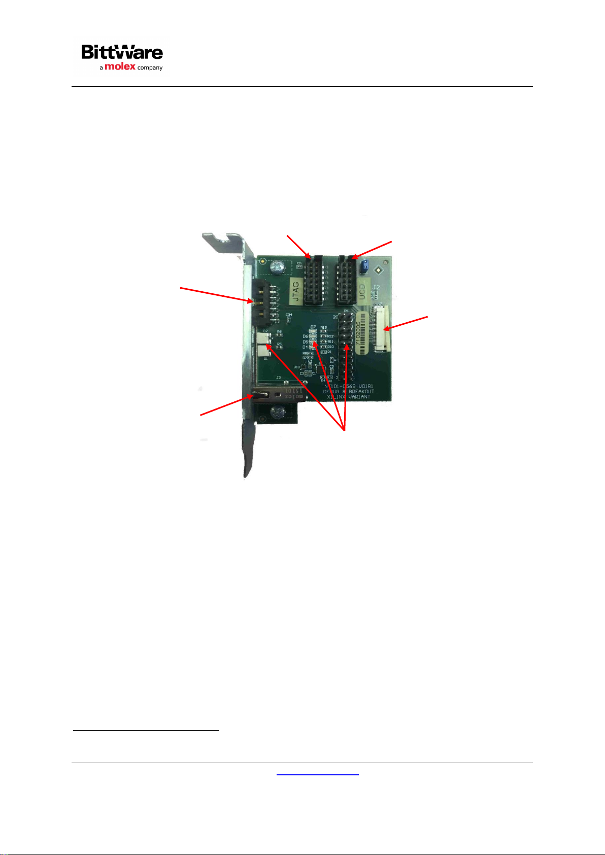
1.1 Product Description.................................................................................................................8
1.2 Feature List .............................................................................................................................8
1.3 Supported JTAG Programming Cables ..................................................................................9
1.4 Supported BittWare FPGA Cards ...........................................................................................9
2. Usage with 250-SoC................................................................................................................11
2.1 Physical Connections............................................................................................................11
2.1.1 Connection to JTAG Programming Cables.......................................................................11
2.1.2 Connection to FPGA Card ................................................................................................11
2.2 JTAG Chain...........................................................................................................................12
2.3 Other Features......................................................................................................................12
2.3.1 I2C Bus..............................................................................................................................12
2.3.2 PS Reset Push Button ......................................................................................................12
3. Usage with 250S+....................................................................................................................14
3.1 Physical Connections............................................................................................................14
3.1.1 Connection to JTAG Programming Cables.......................................................................14
3.1.2 Connection to FPGA Card ................................................................................................14
3.2 JTAG Chain...........................................................................................................................15
3.3 Other Features......................................................................................................................15
3.3.1 FPGA Output Signals (LED Indicator) ..............................................................................15
3.3.2 FPGA Input Signal.............................................................................................................16
3.3.3 FPGA-driven UART...........................................................................................................16

ACC-JTAG-BR Hardware Reference Guide
Rev 1.0 www.bittware.com 6
BittWare Proprietary - Do Not Distribute Without Permission from BittWare
About this Reference Guide
Related Documentation
•BittWare 250-SoC Hardware Reference Guide
•BittWare 250S+ Hardware Reference Guide
Abbreviations and Definitions
▪BIST Built-In Self-Test
▪CFI Common Flash Interface
▪DDR Double Data Rate
▪DMA Direct Memory Access
▪FPGA Field Programmable Gate Array
▪Gb Gigabit
▪GB Gigabyte
▪I2C Inter-IC bus (standard)
▪ILA Integrated Logic Analyzer (Xilinx)
▪IO Input/Outputs
▪IP Intellectual Property
▪JTAG Joint Test Action Group (boundary scan standard)
▪LED Light Emitting Diode
▪MPSoC Multi-Processor System-On-Chip
▪MT/s Mega Transfers per second
▪PSU Power Supply Unit
▪QSPI Quad Serial Peripheral Interface
▪SDRAM Synchronous Dynamic Random-Access Memory
▪PROM Programmable Read-Only Memory
▪PL Programmable Logic
▪PS Processor System
▪USB Universal Serial Bus (standard)
▪VPD Vital Product Data
▪ZIF Zero Insertion Force (connector)

ACC-JTAG-BR Hardware Reference Guide
Rev 1.0 www.bittware.com 8
BittWare Proprietary - Do Not Distribute Without Permission from BittWare
1. ACC-JTAG-BR Overview
1.1 Product Description
The BittWare JTAG Breakout Board allows connectivity of JTAG Programming Cables to compatible
BittWare FPGA Cards. The JTAG Breakout Board comes fitted to a PCI bracket that allows it to be
installed in an adjacent PCIe slot to the paired BittWare FPGA Card.
Figure 1: JTAG Breakout Board
1
1.2 Feature List
The BittWare JTAG Breakout Board has the following features:
•Connectivity to 14-pin JTAG connector standard for JTAG access into the FPGA Card
•Connectivity for optional Push Button on 250-SoC only
•Connectivity for FPGA I2C bus on 250-SoC only
•User FPGA-driven GPIOs on header on 250S+ only
•User FPGA-driven LEDs on 250S+ only
•USB connector for FPGA-driven UART interface on 250S+ only
1
Image shows Bare Board Issue 1 PCB
RESERVED
Internal Xilinx
Platform Flash Cable
Header (P4)
Flexi-cable ZIF
Connector to 250-
SoC Board (J1)
External Xilinx
Platform Flash
Cable Header (P1)
USB to UART Interface
(Not used with 250-SoC)
6 User Programmable
Diagnostic LEDs & P5
Header
(Not Used with 250-SoC)

ACC-JTAG-BR Hardware Reference Guide
Rev 1.0 www.bittware.com 9
BittWare Proprietary - Do Not Distribute Without Permission from BittWare
1.3 Supported JTAG Programming Cables
The BittWare JTAG Breakout Board is compatible with the following JTAG Programming Cables:
•Xilinx Platform Cable USB II
•Xilinx SmartLynq Data Cable
•Diligent JTAG-USB
1.4 Supported BittWare FPGA Cards
The BittWare JTAG Breakout Board is compatible with the following BittWare FPGA Cards:
•250S+
•250-SoC

ACC-JTAG-BR Hardware Reference Guide
Rev 1.0 www.bittware.com 11
BittWare Proprietary - Do Not Distribute Without Permission from BittWare
2. Usage with 250-SoC
2.1 Physical Connections
2.1.1 Connection to JTAG Programming Cables
The JTAG Programming Cables comes supplied with a 14-pin connector and ribbon cable assembly.
Using this cable, the JTAG Programming Cable can be connected to either P1 or P4 of the JTAG
Breakout Board. The P1 and P4 pinout is given in Table 1.
If you are using a V01R1 Bare Board PCB Issue of the JTAG Breakout Card (see Figure 1) you are
required to use the supplied cable labeled ‘JTAG’ rather than the standard point to point cable that is
supplied with the Xilinx JTAG programming tool
The JTAG Programming Cable connects to the JTAG breakout board via P1 or P4 using the correct
point to point cable depending on the bare board PCB number or the flying leads. Both connectors
have the same pin-out this is given below in Table 1.
Pin
Signal Name
Description
1
VCC
3.3V Power
2
GND
No Connect
3
JTAG_TMS
JTAG Test Mode Select
4
GND
Ground
5
JTAG_TCK
JTAG Test Clock
6
GND
Ground
7
JTAG_TDO
JTAG Test Data Out
8
GND
Ground
9
JTAG_TDI
JTAG Test Data In
10
GND
Ground
11
NC
No Connect
12
GND
Ground
13
NC
No Connect
14
GND
Ground
Table 1: Debug & Breakout Card P1 & P4 Pinout
The JTAG Programming Cables typically connect to your chosen programming host via a standard
USB cable.
2.1.2 Connection to FPGA Card
The 250-SoC MPSoC Card is populated with a single row 24-way ZIF connector (J5) located on the
bottom side of the assembly. A ribbon cable is used to connect the 250-SoC to J1 of the JTAG Breakout
Board.

ACC-JTAG-BR Hardware Reference Guide
Rev 1.0 www.bittware.com 12
BittWare Proprietary - Do Not Distribute Without Permission from BittWare
2.2 JTAG Chain
On the 250-SoC, the only device in the JTAG chain is the Xilinx Zynq MPSoC. Within the MPSoC a
user can access the PS, the PL and the QSPI flash memory.
Only the MPSoC device exists in the JTAG chain. The currently supported device is given in Table 2.
Device
Speed Grade
Package
Part Number
XCZU19EG
2
FFVD1760
XCZU19EG-2FFVD1760E
Table 2: JTAG Chain Devices
2.3 Other Features
Some of the LEDs and pins of P5 header connect to the 250-SoC card to perform special functions.
Breakout
P5 Pin
Breakout
LED
Breakout
Signal Name
250-SoC
Signal Name
Description
250-SoC J5 Pin
10
D4
LED2
FPGA_I2C_SCL
I2C clock to
MPSoC & I2C
devices
15
9
D5
LED3
FPGA_I2C_SDA
I2C data to
MPSoC & I2C
devices
16
7
D7
LED5
PB_RST_N
Push Button
Reset to
UCD9090
18
Table 3: Push Button and UCD I2C Bus Signals on Breakout Board
Figure 2: P5 Breakout Board User Signals
When using either the I2C or PB_RST_N, the user will also need to connect to one of the available
grounds on P5 (pins 3, 7, 11, 19, 4, 8, or 20).
2.3.1 I2C Bus
The I2C bus (FPGA_I2C_SDA & FPGA_I2C_SCL) signals are pulled up on the card and give access
to the FPGA I2C bus –See 250-SoC Hardware Reference Guide for details of the devices accessible
on this I2C bus.
2.3.2 PS Reset Push Button
The PB_RST_N is pulled up on the 250-SoC. Users could connect a push button to this signal to
ground the signal with pressed. The 250-SoC card includes a circuit which debounces this input and
creates a pulse on PS_SRST_B to reset the ARM without having to power cycle the card.
LED3 / FPGA_I2C_SDA
LED2 / FPGA_I2C_SCL
LED5 / PB_RST_N

ACC-JTAG-BR Hardware Reference Guide
Rev 1.0 www.bittware.com 14
BittWare Proprietary - Do Not Distribute Without Permission from BittWare
3. Usage with 250S+
3.1 Physical Connections
3.1.1 Connection to JTAG Programming Cables
Please see section 2.1.1.
3.1.2 Connection to FPGA Card
The 250S+ FPGA Card is populated with a single row 24-way ZIF connector (J7) located on the bottom
side of the assembly. A ribbon cable is used to connect the 250S+ to J1 of the JTAG Breakout Board.

ACC-JTAG-BR Hardware Reference Guide
Rev 1.0 www.bittware.com 15
BittWare Proprietary - Do Not Distribute Without Permission from BittWare
3.2 JTAG Chain
On the 250-SoC, the only device in the JTAG chain is the Xilinx Zynq MPSoC. Within the MPSoC a
user can access the PS, the PL and the QSPI flash memory.
Only the FPGA device exists in the JTAG chain. The currently supported devices are given in Table 2
Device
Speed Grade
Package
Part Number
XCKU15P
2
FFVA1156
XCKU15P-2FFVA1156E
Table 4: JTAG Chain Devices
3.3 Other Features
3.3.1 FPGA Output Signals (LED Indicator)
Some of the LEDs and pins of P5 header connect to the 250S+ card to perform special functions.
They are not directly connected to LEDs on the 250S+ board, these are located on the JTAG
Breakout Board when the two boards are connected via connector J7 on the 250S+ and J1 on the
JTAG Breakout Board.
On the JTAG Breakout Board each signal is connected to a pin on header P5 and an LED per Table 5.
Reverse logic is employed on each pin, a zero (0) on the FPGA pin will illuminate the associated LED.
Signal
Name
250S+
JTAG Breakout Board
FPGA
Pin
J7 Pin
P5
LED
Test0
F10
13
Not Connected
D1
Test1
G11
14
2
D2
Test2
H12
15
6
D4
Test3
H11
16
10
D5
Test4
G12
17
14
D6
Test5
F8
18
18
D7
Table 5: GPIO Indicator Signal Mapping
See Figure 2 for pin numbering of P5.
The Test signals associated with the JTAG Breakout Board connect to the FPGA as shown in Table 6.
FPGA Pin
XDC Signal Name
I/O Standard
Direction
F10
test[0]
LVCMOS18
I/O
G11
test[1]
LVCMOS18
I/O
H12
test[2]
LVCMOS18
I/O
H11
test[3]
LVCMOS18
I/O
G12
test[4]
LVCMOS18
I/O
F8
test[5]
LVCMOS18
I/O
Table 6: JTAG Breakout Board Test signals FPGA Pinout
The maximum voltage allowed on each of these I/O signals is 1.8V

ACC-JTAG-BR Hardware Reference Guide
Rev 1.0 www.bittware.com 16
BittWare Proprietary - Do Not Distribute Without Permission from BittWare
3.3.2 FPGA Input Signal
There are two methods available if an external input to the FPGA is required.
1. The user can connect directly to connector J7 on the 250S+ using a suitable flexi-rigid cable such
as Molex part number 15266-0267
2. Attach a modified JTAG Breakout Board where the LED on the GPIO signal to be used has been
depopulated and the signal accessed via the header P5
The maximum voltage allowed on each GPIO signal is 3.3V
3.3.3 FPGA-driven UART
The USB connector on the JTAG Breakout Board can be used to connect to an FPGA-driven UART if
the FPGA design in the 250S+ supports it. The UART signals associated with the JTAG Breakout Board
connect to the FPGA as shown in Table 6.
FPGA Pin
XDC Signal Name
I/O Standard
Direction
L13
bkout_txd
LVCMOS18
In
L12
bkout_rxd
LVCMOS18
Out
K13
bkout_rts
LVCMOS18
In
K12
bkout_cts
LVCMOS18
Out
Table 7: JTAG Breakout Board Test signals FPGA Pinout
The maximum voltage allowed on each of these I/O signals is 1.8V
Table of contents
Other molex Computer Hardware manuals