Smartbitt SBOL50KTIII-3 User manual

UNINTERRUPTIBLE POWER SYSTEM
SERVICE MANUAL
Smartbitt SBOL50KTIII-3, SBOL60KTIII-3,
SBOL90KTIII-3 Tower Model

2

3
1. General Information
1.1 Getting start
This manual is for Smartbitt Ⅲ 30K(L)~200K(L) tower UPS. It can help service person perform the basic
maintenance and repair service.
This manual only focuses on the service section, so you should get the basic operation of the UPS from the
user manual, and make sure you had read and understood the user manual before reading the manual.
The manual includes 9 sections:
● General Information, this section shows you the general information of the service manual.
● Electric Specifications, this section shows you the basic electric specification of the UPS.
● Functional block, this section shows you the major functional block of the UPS.
● Working Principle of the Major Functional Block, this section shows you the working principle of the
major functional block.
● Function explanations for each PCB, this section explains you all the PCBs of the UPS system.
● Interface, this section shows you the LCD interface, including display and setting.
● Trouble Shooting, this section gives you the way to find the problems.
● Test Step, this section tells you how to test the UPS after you repair the unit.
● Appendix, this section shows you the basic waveforms for reference and the basic communication
commands.
1.2 Important Safety Instructions
For qualified service person only.
DO NOT perform any internal service or adjustment of this product unless the technical person is well
trained and experienced. .
Dangerous voltage exists at several points in this product. To avoid personal injury, don't touch any
exposed connections or components while UPS is on.
Turn off the UPS and switch off the input breaker before removing protective case.
AC voltage is always present if the input AC power is still available.
High voltage may exist at DC capacitors. Before removing the protective case, wait for at least five
minutes after turning off the UPS.
Verify input source (voltage and frequency) is within the maximum range before service.

4
2. Electric Specifications
CAPACITY*
30KVA/30KW
60KVA/60KW
100KVA/100KW
120KVA/120KW
180KVA/180KW
200KVA/200KW
INPUT
Voltage
Range
Low Line Loss
110 VAC(L-N) ± 3 % at 50% Load
176 VAC(L-N) ± 3 % at 100% Load
Low Line Comeback
Low Line Loss Voltage + 10V
High Line Loss
300 VAC(L-N) ± 3 %at 50% Load
276 VAC(L-N) ± 3 % at 100% Load
High Line Comeback
High Line Loss Voltage - 10V
Frequency Range
46Hz ~ 54 Hz @ 50Hz system
56Hz ~ 64 Hz @ 60Hz system
Phase
Three phase with Neutral
Power Factor
≧ 0.99 at 100% Load
OUTPUT
Output voltage
208/220/230/240VAC(208 will derating to 90%)
AC Voltage Regulation
± 1%
Frequency Range
(Synchronized Range)
46Hz ~ 54 Hz @ 50Hz system
56Hz ~ 64 Hz @ 60Hz system
Frequency Range (Batt. Mode)
50 Hz ± 0.1 Hz or 60Hz ± 0.1 Hz
Overload
AC mode
100%~110%: 60min; 110%~125%: 10min; 125%~150%:1min;>150% : immediately
Battery mode
100%~110%: 60min; 110%~125%: 10min; 125%~150%:1min;>150% : immediately
Current Crest Ratio
3:1 max
Harmonic Distortion
≦ 2 % @ 100% Linear Load; ≦ 5 % @ 100% Non-linear Load
Transfer
Time
Line Battery
0 ms
Inverter Bypass
0 ms
Inverter ECO
<10 ms
EFFICIENCY
AC mode
> 95.5%
Battery Mode
> 94.5%
BATTERY
Standard
Model
Type
12 V /7 Ah
NA
Numbers
(16+16)pcs*2stri
ng
Recharge Time
7hours
Charging Current
2.0 A ± 10%
(max.)
Charging Voltage
13.65V ± 1%
Long-run
Model
Type
Depending on applications
Numbers
32 - 40
Charging Current
1.0~12.0A
±10%
(Adjustable)
1.0~18.0A
±10%
(Adjustable)
2.0~36.0A ±10% (Adjustable)
Each step 2A
3.0~54.0A ±10% (Adjustable)
Each step 3A
Charging Voltage
13.65VDC± 1%
PHYSICAL
Model
30K
30KL
60KL
100KL
120KL
180KL
200KL
Outline
Dimension, D X W X H
815 x 300 x 1000
979 x 600 x 1600
Net Weight (kg)
207
74
74.2
250
309
311
Packaging
Dimension, D X W X H
920 x 430 x 1205
1125 x 665 x 1800
Gross Weight (kg)
225
94.5
95
278
362
364
ENVIRONMENT
Operation Temperature
0 ~ 40°C (the battery life will down when > 25°C)
Operation Humidity
<95 % and non-condensing
Operation Altitude**
<1000m
Acoustic Noise Level
Less than 65dB
@ 1 Meter
Less than 70dB
@ 1 Meter
Less than 75dB
@ 1 Meter
Less than 75dB
@ 1 Meter
Less than 75dB
@ 1 Meter
Less than 75dB
@ 1 Meter
MANAGEMENT
Smart RS-232 or USB
Supports Windows® 2000/2003/XP/Vista/2008, Windows® 7, Linux, Unix, and MAC
Optional SNMP
Power management from SNMP manager and web browser
* Derate capacity to to 90% when the output voltage is adjusted to 208VAC.
**If the UPS is installed or used in a place where the altitude is above than 1000m, the output power must be derated one percent per 100m.
***Product specifications are subject to change without further notice.

5
3. Functional Block
As a true online UPS, the product applies a double conversion topology, comprising functional blocks as
shown in Figure 3.1
Figure 3.1 Function block Diagram
The CNTL block controls the action of the UPS system. It detects the voltage and current to control PFC
and inverter, also it supplies the protection for the UPS, When the UPS becomes abnormal, in most case,
the CNTL can provide basic information indicating the status of the UPS.
The COMM block provides the communication interface for receiving and executing command from users
via the panel or other communication protocol, also provides the LCD display task.
The PFC blocks are the input stage of the UPS. The blocks convert AC input power into two stable DC
power stored in the BUS capacitor. In the meantime, PFC (Power Factor Correction) will be executed and
allows input current tracking the input voltage waveform. Therefore, the input power factor will be
corrected to 1 to achieve maximum efficiency and produce lowest power pollution to the utility.
The PFC block in battery mode, also called Booster, is used to convert the low voltage DC power to higher
voltage with stable DC power, stored in the BUS capacitor.
The Inverter block is the output stage of the UPS and used to convert DC power from the BUS capacitor
to sine waveform output power.
When the utility is within the acceptable range, the UPS will provide power directly from the utility input
and the Rectifier and PFC will be executed at the same time. When the utility is outside of the acceptable
range, no matter it’s because of input voltage or input frequency, the UPS will shut down the Rectifier and
PFC functions and turn on the Battery Booster. In case of sudden interruption from input utility, the
controller can detect the interruption in very short time. During the short interval of detecting the
interruption, the output power will be provided by the power stored in the BUS capacitor. In this way, there
is no any interruption on output power.
The charger charges the battery when the utility is normal. The charger converts DC input power to DC
power for recharging the battery. The charger’s output current can be setting form 1A to 4A.
The Input and Output EMI section provides EMI filter function. The input and output EMI filters can prevent
the UPS from being interference by external electronic/magnetic noise which is generated by other
electronic system and prevent other systems from the noise generated inside the UPS system.
Input
Input
Breaker
Input EMI Line SCR PFC
Bat SCR
Battery
Charger
SPS Cntl Comm
INV
Maintenance Bypass
Switch
Output EMI
INV Rly
Byp SCR
Output
Bypass
Maintenance Bypass
Single_Input System Principle
Diagram
OVCD relay

6
The SPS generates DC power supply needed by operation of the circuit of the UPS itself. The Bypass
provides a path that utility can power the output directly when the Inverter is not executed. The
Maintenance Bypass provides another path that utility can power the output directly when UPS is in
maintenance status.

7
4. Working Principle of the Major Functional Block
4.1 Switch Power Supply
The Switch Power Supply (SPS) supplies DC power for UPS operation. The input source of the SPS is
the battery, or the output of the charger.
Figure 4.1.1 Basic circuit of power supply for 10K-20K
Figure 4.1.2 Basic circuit of power supply for 30K-80K
Figure 4.1.1 is a flyback converter. When Q1 is on, rectifier diodes (D11/D12) are on open status and
output capacitors (C6/C7) supply currents to the load. The primary coil of the transformer will become a
pure inductor and the primary current will linearly increase to store energy in the coil. When Q1 is off,
primary current will stop and rectifier diodes (D11/D12) will turn to “close” status. It will release the stored
energy from the primary coil of the transformer to the secondary coil to supply loads. At the same time, it
will charge output capacitors including ±12V, +5V, +12V(Fan), and HFPW±.
Figure 4.1.2 is a double tube flyback converter. When Q1 and Q2 are on, rectifier diodes (D11/D12) are
on open status and output capacitors (C6/C7) supply currents to the load. The primary coil of the
transformer will become a pure inductor and the primary current will linearly increase to store energy in
the coil. When Q1 and Q2 are off, primary current will stop and rectifier diodes (D11/D12) will turn to
“close” status. It will release the stored energy from the primary coil of the transformer to the secondary
coil to supply loads. At the same time, it will charge output capacitors including ±12V, +5V, +12V(Fan),
and HFPW±.
The power of ±12V, +5V supplies stable voltage to all kinds of ICs and other devices such as HCT. The
+12V (Fan) is supplied to fans and relays. The HFPW± supplies a high frequency power for the switch
(SCR/IGBT) driver and some other drive boards.
Battery
R LINE
S LI NE
T LINE
SP S_BUS+
SP S_BUS-
Q1
TX +12 V Output
-12 V Output
D1
D2
D3
D4
D5
D6
D7
D8
D11
D12
D11
D12
C3
C4
C6
C7
BUS
D9
D10
C1
C2
D13
C5
R1
Battery
R LINE
S LI NE
T LINE
SP S_BUS+
SP S_BUS-
Q1
Q2
TX +12V Output
-12V Output
D1
D2
D3
D4
D5
D6
D7
D8
D11
D12
D11
D12
C3
C4
C6
C7
BUS
D9
D10
C1
C2
D13
D14

8
4.2 PFC/Booster
Figure 4.2 PFC/Booster
As shown in the Figure 4.2, when Q1/Q2 is on and D1/D2 is off, the current will increase to store energy
in choke(L1/L2). When the Q1/Q2 is off and D1/D2 is on, the choke will release energy. Therefore, we
can control the current in chokes (input current) by regulating the time of Q1/Q2 on and off. There are three
independent PFC/Booster for each phase.
4.3 Inverter
The input of the three-level inverter topology is two DC voltages, and the output is an AC voltage, as
shown in the Figure 4.3. When Q1 and Q2 are on, Q3 and Q4 are off, the voltage of the middle point
bridge is +BUS. When Q1 and Q2 are off, Q3 and Q4 are on, the voltage of the middle point bridge is –
BUS. We can get any voltage waveform between ±BUS voltage from LC filter output by regulating the
duty cycle of Q1/Q2/Q3/Q4, including sine wave form.
Figure 4.3 three-level inverter
N
Q1
Q2
UBUS+
UBUS-
R/S/T
Battery
L1
D2
D1
C1
C2
N
L2
Q3
Q4
Q5
Q6
INV OUTPUT
+BUS
-BUS
N
C1
L1
C2 C3
D1
D2
Q1
Q2
Q3
Q4

9
4.4 Charger
The function of charger is to charge and maintain the batteries at fully charged condition. The charger
charges the batteries with a constant current at initial stage. At the same time, the battery voltage keeps
increasing until reaching the constant charge voltage point. Then, the charge current will decrease
accordingly, now it’s in second stage. After one hour of constant voltage charging, the charge voltage will
change to floating charge voltage, in general, the charger will control the output voltage at a constant
level (13.65V±1% per battery) to optimize battery recharge time and prolong the lifetime of batteries
without overcharging.
As shown in the Figure 4.4, the battery charger applies buck converter.
Figure 4.4 Topology of the charger
4.5 EMI Board
Input EMI board is connected between utility and the input of rectifier. Output EMI board is connected
between the output of inverter and output terminal block.
Figure 4.5 Topology of the input/output EMI
+BUS
N
-BUS
BAT+
N
BAT-
C1
C2
C3
C4
Q1
Q2
D1
D2
L1
L2
D3
D4
Cx
Cx
Cx
Cy Cy
Cy
Cy
Cy
Cy
Cy
Cy
Cy
Cy
Cy
I P/ R
I P/ S
I P/ T
I P/ N
OP/ R
OP/ S
OP/ T
OP/ N
L1
F1
F2
F3

10
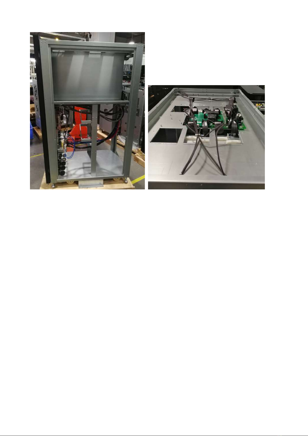
n 5. Picture of the UPS
30k picture single input dual input

11
30k UPS inner picture
60K picture

12
60K picture
60K unit inner picture

13
Front panel
Rear panel Left panel
100K~200K picture
14
Right side panel Top side panel
100K~200K picture

15
6. Function explanations for each PCB
Table 5.1 PCBA information of Smartbitt 3-3 10~80k
Ite
m
Mode
l
Part number
Function
Picture
1
30K
31-531408-
XXG
INV board
2
30K
31-531407-
XXG
PFC board
3
30K
~
200K
72-300745-
XXG
INV Control
board
4
30K
~
200K
72-300744-
XXG
PFC Control
board

16
5
30K
71-304525-
XXG
Input fuse EMI
board
6
30K
Rack
72-300820-
XXG(LCD)
Communicatio
n
board
30K
60K
Tow e
r
72-300746-
XXG(LCD)
60K
~
200K
tower
72-300773-
XXG(Touch
panel)
7
30K
~
200K
31-531225-
XXG
Parallel board
8
30K
31-531366-
XXG
SPS board
9
60K
~
31-531025-
01G
R PFC board

17
200K
31-531252-
XXG
ST PFC board
10
60K
~
200K
31-531026-
XXG
INV Board
11
60K
~
200K
31-531253-
XXG
AC IN Board
12
60K
~
200K
31-531254-
XXG
Bypass board

18
13
60K
~
200K
31-531255-
XXG
Charger board
14
60K
~
200K
71-600400-
XXG
Charger fuse
board
15
30K
~
200K
71-304252-
XXG
SNMP card
power supply
board
16
30K
~
200K
71-300194-
XXG
EMBS board

19
17
30K
~
200K
71-303357-
XXG
(71-304615-
00G for
advance
communicatio
n board)
Touch panel
power board
Note: “XX” in the serial number is the version of the PCB. It may be modified according to releasing
version in the future.

20
7. Interface
7.1 LED Display
Table 6.1 LED Display
MODE LED
Bypass
Line
Battery
Fault
UPS Startup
●
●
●
●
No output
○
○
○
○
Bypass mode
●
○
○
○
Line mode
○
●
○
○
Battery mode
○
○
●
○
Battery test
●
●
●
○
ECO mode
●
●
○
○
CVCF mode
○
●
○
○
Fault mode
○
○
○
●
●: means LED is lighting.
○: means LED is faded.
7.2 LCD Display
Figure 6.1 LCD Display
This manual suits for next models
2
Table of contents
Other Smartbitt UPS manuals


Popular UPS manuals by other brands


Xtreme Power Conversion
Xtreme Power Conversion NXRi-6KL User & installation manual

Eaton
Eaton 93PM IBC-L Installation and operation manual

Toshiba
Toshiba 4200FA Series Installation planning guide

Liebert
Liebert UPStation S VCR232C Installation and instruction manual

Dell
Dell UPS 2700R Series Getting Started With Your System

socomec
socomec DELPHYS MX manual


