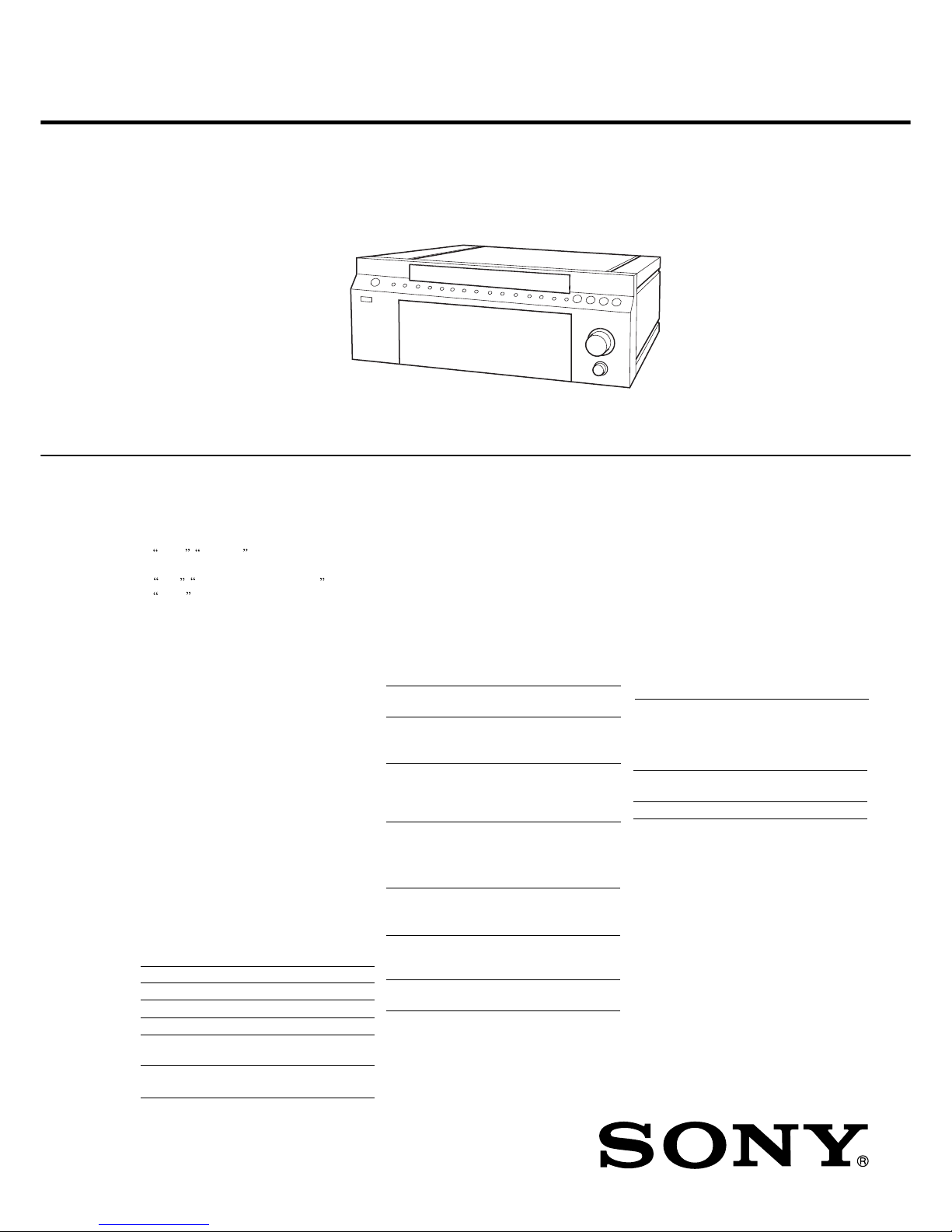
Sony TA-DA9000ES User manual

SERVICE MANUAL
MULTI-CANNEL INTEGRATED AMPLIFIER
SPECIFICATIONS
TA-DA9000ES
Ver 1.0 2003.10
9-961-291-01 Sony Corporation
2003J05-1 Home Audio Company
C2003.10 Published by Sony Engineering Corporation
AEP Model
E Model
– Continued on next page –
This amplifier incorporates Dolby* Digital and Pro
Logic Surround and the DTS** Digital Surround
System.
*Laboratories.
Dolby ,Pro Logic and the double-D symbol are
trademarks of Dolby Laboratories.
** DTS ,DTS-ES Extended Surround , and
Neo:6 are trademarks of Digital Theater Systems,
Inc.
Manufactured under license from Dolby
Amplifier section
POWER OUTPUT
Rated Power Output at Stereo Mode
1)
(8 ohms, 20 Hz −20 kHz, THD 0.15%)
200 W + 200 W
(4 ohms, 20 Hz −20 kHz, THD 0.15%)
220 W + 220 W
Reference Power Output
(8 ohms, 1 kHz, THD 0.09%)
FRONT
2)
: 200 W + 200 W
CENTER
2)
: 200 W
SURR
2)
: 200 W + 200 W
SURR BACK
2)
: 200 W + 200 W
(4 ohms, 1 kHz, THD 0.09%)
FRONT
2)
: 220 W + 220 W
CENTER
2)
: 220 W
SURR
2)
: 220 W + 220 W
SURR BACK
2)
: 220 W + 220 W
1) Depending on the sound field settings and the
source, there may be no sound output.
2) Measured under the following conditions:
Frequency response
Inputs (Analog)
3) Input shorted and sealed at VOL MAX.
4) Weighted network + 20 kHz LPF, input level.
Area code Power requirements
CEL 230 V AC, 50/60 Hz
TW 110 V AC, 60 Hz
KR 230 V AC, 60 Hz
PHONO RIAA equalization curve
±0.5 dB
Power Amp Block 10 Hz −50 kHz
±3 dB (8 ohms)
PHONO Sensitivity: 3.5 mV
Impedance: 50 kilohms
S/N
3)
: 90 dB (A, 40 mV
4)
)
CD/SACD, TAPE,
MD/DAT, DVD, LD,
TV/SAT, VIDEO 1, 2,
3, 4, 5
Sensitivity: 170 mV
Impedance: 50 kilohms
S/N
3)
: 100 dB (A, 2V
4)
)
Inputs (Digital)
Outputs
EQUALIZER
Video section
Inputs/Outputs
Video: 1 Vp-p, 75 ohms
S-video: Y: 1 Vp-p, 75 ohms
C: 0.286 Vp-p, 75 ohms
COMPONENT VIDEO:Y: 1 Vp-p, 75 ohms
P
B
/C
B
/B-Y: 0.7 Vp-p, 75
ohms
P
R
/C
R
/R-Y: 0.7 Vp-p, 75
ohms
CD/SACD, DVD, LD,
VIDEO 1, TV/SAT
(Coaxial)
Impedance: 75 ohms
S/N: 100 dB
(A Network, 20 kHz LPF)
CD/SACD, DVD, LD,
TV/SAT, MD/DAT,
VIDEO1, 3 (Optical)
S/N: 100 dB
(A Network, 20 kHz LPF)
TAPE, MD/DAT
(REC OUT), VIDEO
1, 2, 3 (AUDIO OUT)
Voltage: 170 mV
Impedance: 2.2 kilohms
FRONT L/R,
CENTER,
SURROUND L/R,
SURROUND BACK
L/R, SUB WOOFER
Voltage: 2 V
Impedance: 220 ohms
Gain levels ±10 dB, 1 dB step

2
TA-DA9000ES
Notes on chip component replacement
• Never reuse a disconnected chip component.
• Notice that the minus side of a tantalum capacitor may be dam-
aged by heat.
SAFETY-RELATED COMPONENT WARNING!!
COMPONENTS IDENTIFIED BY MARK 0OR DOTTED
LINE WITH MARK 0ON THE SCHEMATIC DIAGRAMS
AND IN THE PARTS LIST ARE CRITICAL TO SAFE
OPERATION. REPLACE THESE COMPONENTS WITH
SONY PARTS WHOSE PART NUMBERS APPEAR AS
SHOWN IN THIS MANUAL OR IN SUPPLEMENTS PUB-
LISHED BY SONY.
: LEAD FREE MARK
Unleaded solder has the following characteristics.
• Unleaded solder melts at a temperature about 40 ˚C higher than
ordinary solder.
Ordinary soldering irons can be used but the iron tip has to be
applied to the solder joint for a slightly longer time.
Soldering irons using a temperature regulator should be set to
about 350 ˚C.
Caution: The printed pattern (copper foil) may peel away if the
heated tip is applied for too long, so be careful!
• Strong viscosity
Unleaded solder is more viscou-s (sticky, less prone to flow)
than ordinary solder so use caution not to let solder bridges oc-
cur such as on IC pins, etc.
• Usable with ordinary solder
It is best to use only unleaded solder but unleaded solder may
also be added to ordinary solder.
i.LINK section
Pin 4 pins
Transmission speed S200 (Maximum data
transmission speed 200
Mbps)
Transmission protocol A/M transmission protocol
Format (input) Super Audio CD* (DSD
PLAIN)
2 channel linear PCM (IEC-
60958-3)
Sampling frequency: 44.1
kHz
* Conforms to the copy protection technology of
DTLA (Revision 1.2).
General
Power requirements
Power consumption 600 W
Power consumption (during standby mode)
1 W
AC outlets
Dimensions 430 ×238 ×480 mm
including projecting parts and
controls
Mass (Approx.) 28.5 kg
Supplied accessories
AC power coad (1)
Easy Setup Guide (1)
Remote commander RM-LJ312 (1)
Operating Instructions for RM-LJ312 (1)
R6 (size-AA) batteries (3)
Design and specifications are subject to change
without notice.
Area code Power requirements
AEP 230 V AC, 50/60 Hz
Taiwan 110 V AC, 60 Hz
Korean 220 V AC, 60 Hz
Area code AC outlets
AEP 1 switched, 100 W MAX
except AEP −(no AC outlet)
Area code Power requirements

3
TA-DA9000ES
1. SERVICING NOTES ............................................... 5
2. GENERAL
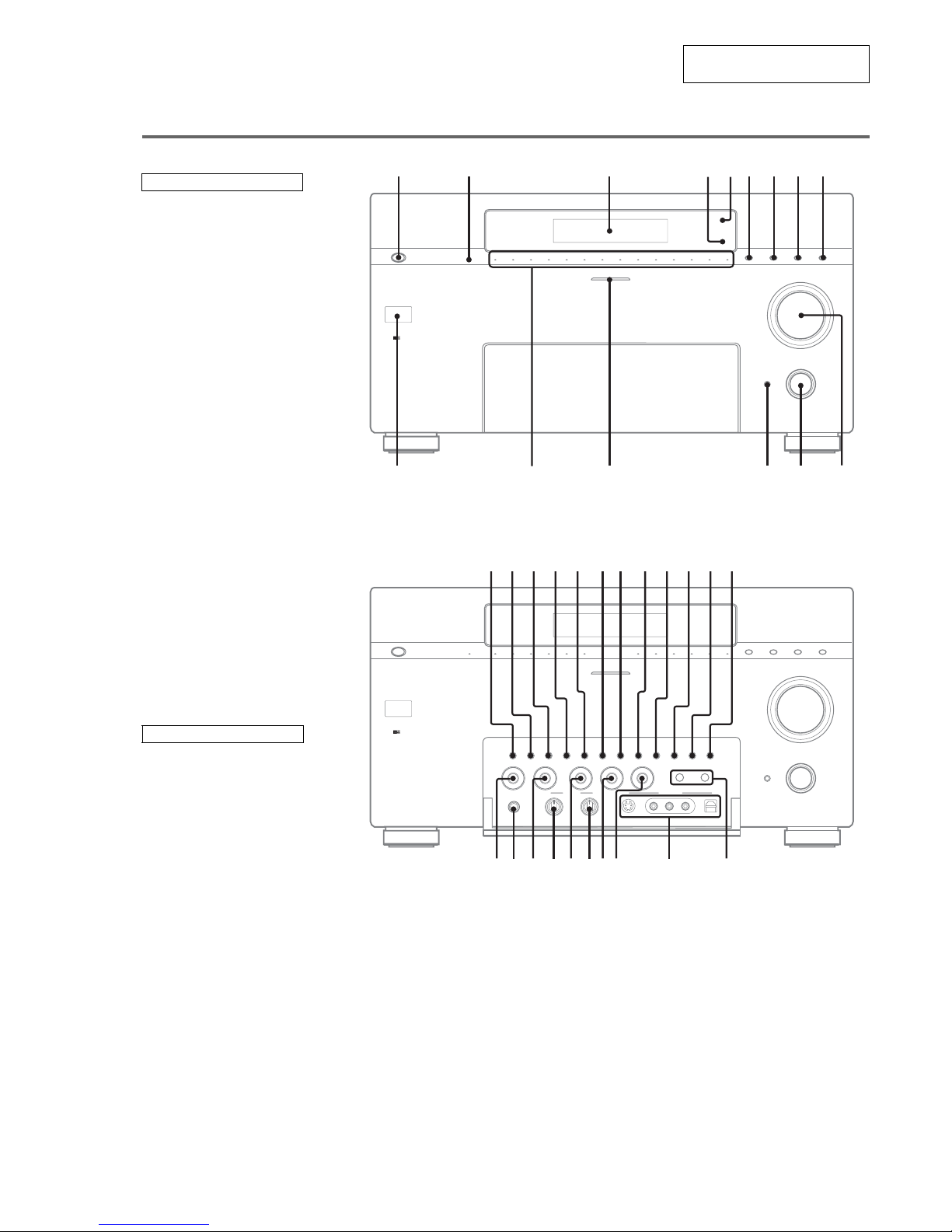
Location of Controls ....................................................... 9
3. DISASSEMBLY
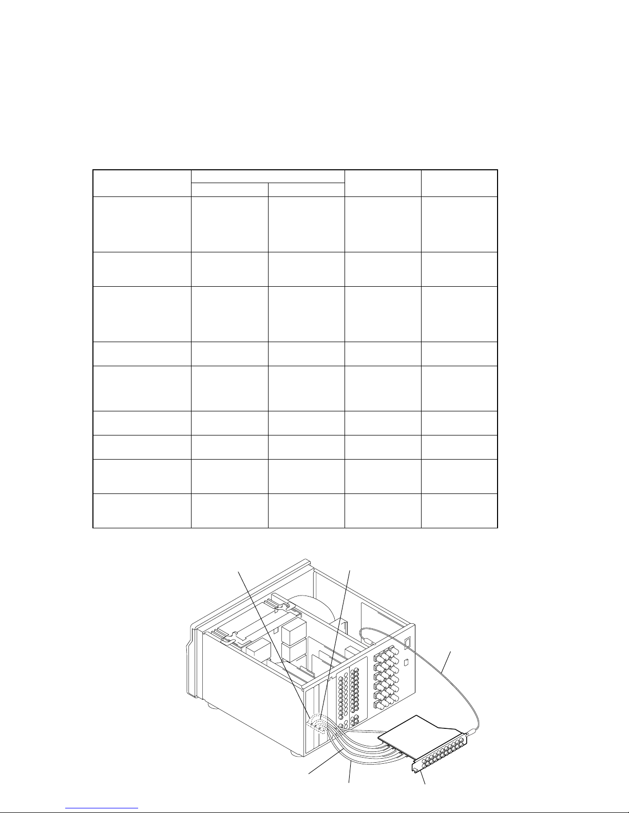
3-1. Disassembly Flow ........................................................... 11
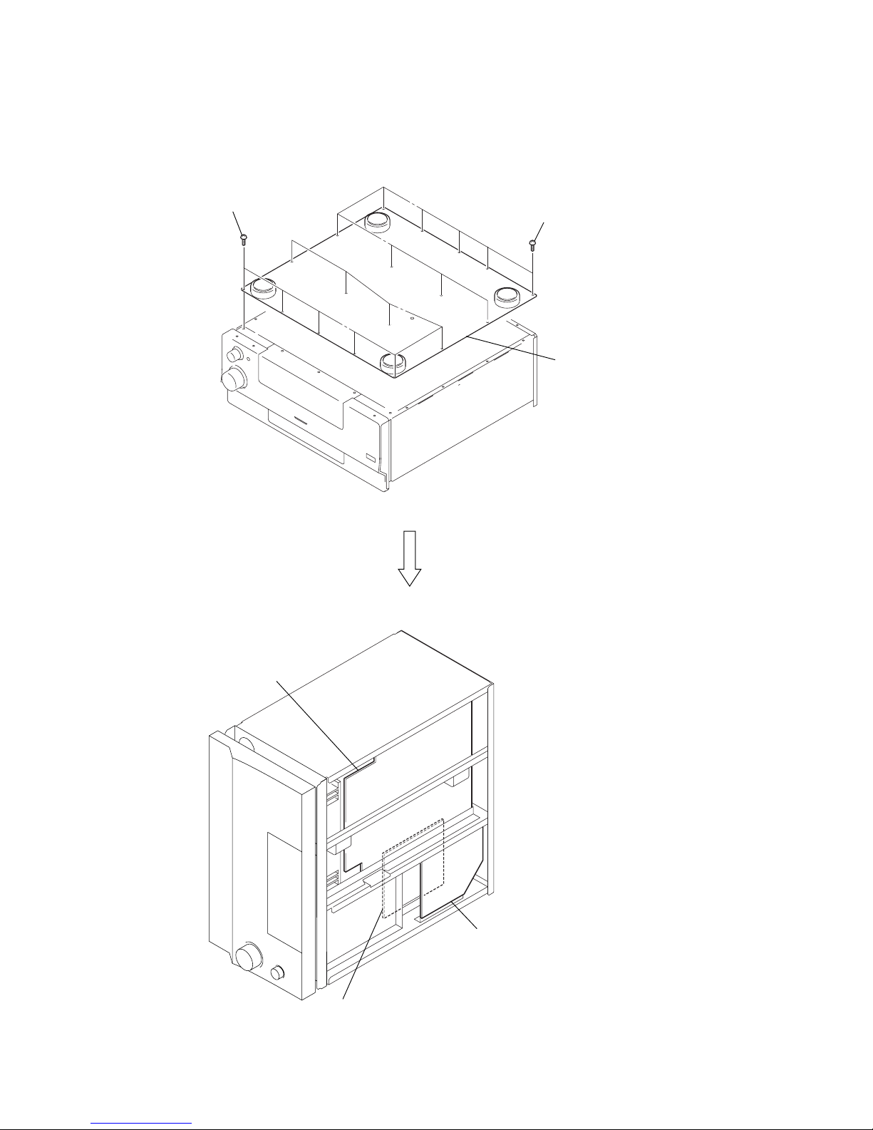
3-2. Case (Top)/(Side-L)/(Side-R) ......................................... 12
3-3. Bracket (J)/(P-B) ............................................................. 12
3-4. AMP Board Block........................................................... 13
3-5. COMPONENT Board Section........................................ 13
3-6. S-VIDEO/VIDEO Board Block ..................................... 14
3-7. SUB Board, PREOUT Board, MAIN Board.................. 14
3-8. I. LINK Board, DIGITAL Board .................................... 15
3-9. MOTHER Board Section ................................................ 15
3-10. MOTHER Board ............................................................. 16
4. TEST MODE.............................................................. 17
5. ELECTRICAL ADJUSTMENTS......................... 20
6. DIAGRAMS
6-1. Block Diagram – AUDIO INPUT Section – ................. 23
6-2. Block Diagram – A/D CONVERTER Section – ........... 24
6-3. Block Diagram – DIGITAL INPUT Section –.............. 25
6-4. Block Diagram – I. LINK Section –.............................. 26
6-5. Block Diagram – DSP Section – ................................... 27
6-6. Block Diagram – DIGITAL AUDIO Section – ............. 28
6-7. Block Diagram – AUDIO OUTPUT Section – ............. 29
6-8. Block Diagram – POWER AMP Section – ................... 30
6-9. Block Diagram – VIDEO INPUT/OUT Section – ........ 31
6-10. Block Diagram – COMPONENT VIDEO Section – .... 32
6-11. Block Diagram – DISPLAY/CONTROL Section – ...... 33
6-12. Block Diagram – POWER SUPPLY Section – ............. 34
6-13. Note for Printed Wiring Boards
and Schematic Diagrams ................................................ 35
6-14. Printed Wiring Board
– DIGITAL Board (Component Side) – ......................... 36
6-15. Printed Wiring Board
– DIGITAL Board (Conductor Side) –........................... 37
6-16. Schematic Diagram – DIGITAL Board (1/11) –........... 38
6-17. Schematic Diagram – DIGITAL Board (2/11) –........... 39
6-18. Schematic Diagram – DIGITAL Board (3/11) –........... 40
6-19. Schematic Diagram – DIGITAL Board (4/11) –........... 41
6-20. Schematic Diagram – DIGITAL Board (5/11) –........... 42
6-21. Schematic Diagram – DIGITAL Board (6/11) –........... 43
6-22. Schematic Diagram – DIGITAL Board (7/11) –........... 44
6-23. Schematic Diagram – DIGITAL Board (8/11) –........... 45
6-24. Schematic Diagram – DIGITAL Board (9/11) –........... 46
6-25. Schematic Diagram – DIGITAL Board (10/11) –......... 47
6-26. Schematic Diagram – DIGITAL Board (11/11) –......... 48
6-27. Schematic Diagram – MAIN Board (1/3) – .................. 49
6-28. Schematic Diagram – MAIN Board (2/3) – .................. 50
6-29. Schematic Diagram – MAIN Board (3/3) – .................. 51
6-30. Printed Wiring Board
– MAIN Board (Component Side) – .............................. 52
6-31. Printed Wiring Board
– MAIN Board (Conductor Side) – ................................ 53
6-32. Printed Wiring Board
– SUB Board (Component Side) – ................................. 54
6-33. Printed Wiring Board
– SUB Board (Conductor Side) – ................................... 55
6-34. Schematic Diagram – SUB Board (1/2) – ..................... 56
6-35. Schematic Diagram – SUB Board (2/2) – ..................... 57
6-36. Printed Wiring Board
– I. LINK Board (Component Side) – ............................ 58
6-37. Printed Wiring Board
– I. LINK Board (Conductor Side) –.............................. 59
6-38. Schematic Diagram – I. LINK Board (1/4) –................ 60
6-39. Schematic Diagram – I. LINK Board (2/4) –................ 61
6-40. Schematic Diagram – I. LINK Board (3/4) –................ 62
6-41. Schematic Diagram – I. LINK Board (4/4) –................ 63
6-42. Printed Wiring Board – PREOUT Board – ................... 64
6-43. Schematic Diagram – PREOUT Board – ...................... 65
6-44. Printed Wiring Board – VIDEO Board –....................... 66
6-45. Schematic Diagram – VIDEO Board – ......................... 67
6-46. Printed Wiring Board – S-VIDEO Board –................... 68
6-47. Schematic Diagram – S-VIDEO Board –...................... 69
6-48. Printed Wiring Board
– COMPONENT Section (Component Side) –.............. 70
6-49. Printed Wiring Boards
– COMPONENT Section (Conductor Side) – ............... 71
6-50. Schematic Diagram
– COMPONENT Section (1/4) –.................................... 72
6-51. Schematic Diagram
– COMPONENT Section (2/4) –.................................... 73
6-52. Schematic Diagram
– COMPONENT Section (3/4) –.................................... 74
6-53. Schematic Diagram
– COMPONENT Section (4/4) –.................................... 75
6-54. Printed Wiring Board
– MOTHER Board (Component Side) – ........................ 76
6-55. Printed Wiring Board
– MOTHER Board (Conductor Side) – .......................... 77
6-56. Schematic Diagram – MOTHER Board (1/3) –............ 78
6-57. Schematic Diagram – MOTHER Board (2/3) –............ 79
6-58. Schematic Diagram – MOTHER Board (3/3) –............ 80
6-59. Schematic Diagram – AMP Board (1/5) – .................... 81
6-60. Schematic Diagram – AMP Board (2/5) – .................... 82
6-61. Schematic Diagram – AMP Board (3/5) – .................... 83
6-62. Schematic Diagram – AMP Board (4/5) – .................... 84
6-63. Schematic Diagram – AMP Board (5/5) – .................... 85
6-64. Printed Wiring Board
– AMP Board (Component Side) – ................................ 86
6-65. Printed Wiring Board
– AMP Board (Conductor Side) – .................................. 87
6-66. Printed Wiring Board – FCOIL Board – ....................... 88
6-67. Schematic Diagram – FCOIL Board – .......................... 89
6-68. Printed Wiring Board – RCOIL Board –....................... 90
6-69. Schematic Diagram – RCOIL Board –.......................... 91
6-70. Printed Wiring Boards – SP Section –........................... 92
6-71. Schematic Diagram – SP Section – ............................... 93
6-72. Printed Wiring Board – DISPLAY Section – ................ 94
6-73. Schematic Diagram – DISPLAY Section – ................... 95
6-74. Printed Wiring Boards – PANEL Section – .................. 96
6-75. Schematic Diagram – PANEL Section – ....................... 97
6-76. Printed Wiring Board
– DC Board (Component Side) – ................................... 98
6-77. Printed Wiring Board
– DC Board (Conductor Side) – ..................................... 99
6-78. Schematic Diagram – DC Board – ............................... 100
6-79. Printed Wiring Board – AC Board –............................. 101
6-80. Schematic Diagram – AC Board –................................ 102
6-81. IC Pin Function Description .......................................... 119
TABLE OF CONTENTS

4
TA-DA9000ES
7. EXPLODED VIEWS
7-1. Case Section ................................................................... 141
7-2. Disp Board Section ........................................................ 142
7-3. Volume Section .............................................................. 143
7-4. Panel (Door) Section...................................................... 144
7-5. Front Panel Section ........................................................ 145
7-6. Base Panel Section ......................................................... 146
7-7. AMP Board Section ....................................................... 147
7-8. Component Board Section ............................................. 148
7-9. Main Board Section ....................................................... 149
7-10. Digital/I. Link Board Section ........................................ 150
7-11. Back Panel Section......................................................... 151
7-12. Transformer Section....................................................... 152
7-13. MOTHER Board Section ............................................... 153
8. ELECTRICAL PARTS LIST .............................. 154

5
TA-DA9000ES
SECTION 1
SERVICING NOTES
NOTES ON REPLACEMENT OF I. LINK BOARD
New part of microcomputer (IC3002) and EEPROM (IC3001) on the I. LINK board cannot be used. Therefore, if the mounted I. LINK
board (A-4733-835-A) is replaced, exchange new microcomputer and new EEPROM with that used before the replacement.
OPERATION CHECK OF STANDING BOARDS ON THE MOTHER BOARD
The standing boards connected to the MOTHER board via the connectors can be operated using the jig with the standing boards discon-
nected from the MOTHER board.
In such a case, for the board with the bracket (back panel), remove the board together with the bracket from the MOTHER board, and
connect the bracket to the chassis using a cable attached with alligator clips for GND connection.
Board Ref. No. of connector Pitch/Pin Part No. of jig
Each board MOTHER board
DIGITAL board CN2001 CNS801 1.25mm/20 pin J-2501-260-A
CN2002 CNS802 1.25mm/20 pin J-2501-260-A
CN2003 CNS803 1.25mm/16 pin J-2501-258-A
CN2004 CNS804 1.25mm/18 pin J-2501-259-A
CN2005 CNS805 1.25mm/20 pin J-2501-260-A
I. LINK board CN3501 CNS806 1.25mm/16 pin J-2501-258-A
CN3502 CNS807 1.25mm/18 pin J-2501-259-A
CN3503 CNS808 1.25mm/6 pin J-2501-253-A
MAIN board CN101 CNS810 1.25mm/14 pin J-2501-257-A
CN102 CNS811 1.25mm/14 pin J-2501-257-A
CN103 CNS809 1.25mm/8 pin J-2501-254-A
CN104 CNS825 1.25mm/20 pin J-2501-260-A
CN105 CNS824 1.25mm/10 pin J-2501-255-A
PREOUT board CN1201 CNS822 1.25mm/16 pin J-2501-258-A
CN1203 CNS823 1.25mm/10 pin J-2501-255-A
SUB board CN1003 CNS812 1.25mm/14 pin J-2501-257-A
CN1002 CNS813 1.25mm/14 pin J-2501-257-A
CN1001 CNS814 1.25mm/8 pin J-2501-254-A
CN1006 CNS826 1.25mm/12 pin J-2501-256-A
VIDEO board CN302 CNS816 1.25mm/18 pin J-2501-259-A
CN301 CNS815 1.25mm/8 pin J-2501-254-A
S-VIDEO board CN402 CNS817 1.25mm/20 pin J-2501-260-A
CN401 CNS818 1.25mm/6 pin J-2501-253-A
COMPONENT board CN1303 CNS819 1.25mm/20 pin J-2501-260-A
CN1302 CNS820 1.25mm/16 pin J-2501-258-A
CN1301 CNS821 1.25mm/20 pin J-2501-260-A
AMP board CN1501 CN824 2.5mm/20 pin J-2501-262-A
CN1507 CN816 2.5mm/6 pin J-2501-261-A
CN1508 CN815 2.5mm/6 pin J-2501-261-A
connecting jig connecting jig
aligator clip
board
Example of Connection

6
TA-DA9000ES
Note: Follow the disassembly procedure in the numerical order given.
– BOTTOM VIEW –
1
nine screws
(BV3
×
8)
2
nine screws
(BV3
×
8)
3
bottom plate
mother board
FSP board
DC board
NOTE:
•
FSP board can be removed in this state.
•
In the same state after removing a FSP board,
the check of DC board can be performed.

7
TA-DA9000ES
DIGITAL BOARD SERVICE POSITION
Note: Case (top) and Case (side-L)/(side-R) are removed.
AMP BOARD SERVICE POSITION
digital board
Please place a sheet
for insulation.
aligator clip
Connect jig (J-2501-253-A)
to the AMP board (CN1507)
and mother board (CN816).
Connect jig (J-2501-260-A)
to the AMP board (CN1501)
and mother board (CN824).
Connect jig (J-2501-253-A)
to the AMP board (CN1508)
and mother board (CN815).

8
TA-DA9000ES
DISP BOARD SERVICE POSITION
Note: Please open a front panel on the right hand side of the set front.
DISP board
front panel section
• MODEL IDENTIFICATION
– Back Panel –
PART No.
Model PART No.
AEP model 4-248-144-1[]
Korean model 4-248-144-2[]
Taiwan model 4-248-144-3[]

9
TA-DA9000ES
SECTION 2
GENERAL This section is extracted from
instruction manual.
LOCATION OF CONTROLS
Main unit
A.F.D. 7
BASS ej
DECODE PRIORITY wf
Digital Cinema Sound indicator 5
DIMMER qh
DIRECT wg
DIRECT indicator 2
DISPLAY wd
Display 3
ENTER wa
Input indicators qf
INPUT MODE qs
INPUT SELECTOR qa
IR receptor qg
MAIN MENU ed
MASTER VOLUME q;
MENU ea
MOVIE 8
MULTI CH IN 1/2 wh
MULTICHANNELDECODING
indicator qd
MUSIC 9
NIGHT MODE qk
ON SCREEN ql
PHONES jack eh
REC OUT SELECTOR +/−wk
SB DEC indicator 4
SLEEP qj
SPEAKERS FRONT switch ef
SPEAKERSSURROUNDswitches
SURR BACK DECODING wj
TEST TONE w;
TREBLE eg
USER PRESET ws
VIDEO 5 INPUT jacks wl
2CH 6
?/1 (power) 1
−/+ e;
ALPHABETICAL ORDER
NUMBERS AND SYMBOLS
v
1 2 354 7 8 9
qdqg qaqs 0
qf
wg wh wjqlqkqjqh w; wa ws wd wf
eh efeg edej es wleae; wk
6

10
TA-DA9000ES
– Remote Commander –
?/1
1
Press to turn the receiver on or off.
AV ?/1
2
Press to turn on or off the components that
the remote is programmed to operate. For
details on programming procedure, see
P rogramming the remote on page 16.
If you press the ?/1 switch (1) at the
same time, it will turn off the main
component and other Sony audio/video
components (SYSTEM STANDBY).
Note
The function of the AV ?/1 switch changes
automatically each time you press INPUT
SELECTOR (4). Depending on thecomponent,
the above operation may not be possible or may
operate differently than described.
AV MENU
ws
Press to display the menus of the VCR,
DVD player, or satellite tuner on the TV
screen. Then use the control button to
perform the menu operations.
Control button
w;
After pressing MAIN MENU, TOP
MENU/GUIDE, or AV MENU, move the
control button up, down, left or right to
select the settings. When you press TOP
MENU/GUIDE or AV MENU, press the
button to enter the selection.
To perform menu operations on the VCR,
DVD player, or SAT tuner, do the
procedure below. If you do not do this, the
cursor buttons merely operate the receiver.
1
Press INPUT SELECTOR and move the
easy scroll key to select the input, then
press the key to enter the selection.
2
Press MAIN MENU, TOP MENU/
GUIDE, or AV MENU.
The CURSOR TYPE list appears. If the
list has disappeared before you go on to
step 3, press any of the cursor buttons to
restore the list.
3
Move the easy scroll key to select the
component that you selected in step 1,
then press the key to enter the selection.
+
—
+
—
+
—
O
AV ?/1TV ?/1
SOUND FIELD
TOP MENU/GUIDE AV MENU
DISPLAY
TV VOL TV CH TV/VIDEO
WIDE
MAIN
MENU
ON SCREEN
RETURN/EXIT
MASTER
VOL
MUTING
INPUT SELECTOR
SYSTEM STANDBY
RM SET UP
?/1
HX x
.> m M
Ii
wj
wa
8
qa
0
wg
wf
9
qg
wd
wh
ql
qk
qf
qj
w;
qs
7
qh
qd
ws
4
1
5
6
3
2
DISPLAY
ql
Press to select information displayed on the
TV screen.
Display window
3
The current status of the selected
component or a list of selectable items
appears here.
Note
Characters other than letters of the alphabet or
numbers may be displayed incorrectly on the
remote, even if they appear correctly in the
display window on the main unit.
Easy scroll key
wg
While displayinga list, move up or downto
select an item from the list, and then press
to enter the selection.
INPUT SELECTOR
4
Press to display the input (component) list.
MAIN MENU
qd
Press repeatedly to select a menu
(SURROUND, etc.) for the receiver.
MASTER VOL +/–
qa
Press to adjust the volume level of all
speakers at the same time.
MUTING
q;
Press to mute the sound.
ON SCREEN
qf
Press to display the menus of the receiver
on the TV screen.
RETURN O/EXIT
qk
Press to return to the previous menu or exit
the menu while the menu or guide of the
VCR, DVD player, or satellite tuner is
displayed on the TV screen.
RM SET UP
5
Press to display the set up list.
SOUND FIELD
wh
Press to display the sound field list.
TOP MENU/GUIDE
wa
Press to display the menu or guide of the
DVD player or satellite tuner on the TV
screen. Then use the control button to
perform the menu operations.
TV ?/1
wj
Press to turn TV on or off.
TV/VIDEO
qs
Press to change the input mode of the TV.
TV CH +/–
qh
Press to switch the channel of TV.
TV VOL +/–
qj
Press to adjust the volume of TV.
WIDE
qg
Press to switch the TV to the wide mode.
I/i
6
Press to change the information displayed
on the display. Press the Ibutton
repeatedly to display the RECEIVER
menu, press the ibutton repeatedly to
display the SUB menu or NUM menu.
Inthe NUM menu,move the easy scroll key
to select the numeric value, then press the
key to enter the selection.
H
wd
Press to start play of the playback medium.
X
9
Press to pause play or recording, or press to
start recording when the component is in
recording standby.
x
8
Press to stop play.
./>
wf
Press to skip tracks.
m/M
7
Press to fast-forward or rewind, or search
tracks in the forward or backward direction.

11
TA-DA9000ES
• This set can be disassembled in the order shown below.
3-1. DISASSEMBLY FLOW
SECTION 3
DISASSEMBLY
SET
3-2. CASE (TOP)/(SIDE-L)/(SIDE-R)
(Page 12)
3-3. BRACKET (J)/(P-B)
(Page 12)
3-4. AMP BOARD BLOCK
(Page 13) 3-5. COMPONENT BOARD SECTION
(Page 13)
3-6. S-VIDEO/VIDEO BOARD BLOCK
(Page 14)
3-7. SUB BOARD, PREOUT BOARD, MAIN BOARD
(Page 14)
3-8. I.LINK BOARD, DIGITAL BOARD
(Page 15)
3-9. MOTHER BOARD SECTION
(Page 15)
3-10. MOTHER BOARD
(Page 16)

12
TA-DA9000ES
3-3. BRACKET (J)/(P-B)
Note: Follow the disassembly procedure in the numerical order given.
3-2. CASE (TOP)/(SIDE-L)/(SIDE-R)
6
four screws
2
two screws
1
three screws
(BV/ring)
4
four screws
5
case (side-L)
3
case (top)
7
case (side-R)
8
bracket (P-B)
7
three screws
(BV3
×
8)
1
four screws
(BV3
×
8)
2
bracket (J)
5
three screws
(BV3
×
8)
3
three screws
(BV3
×
8)
4
bracket (D-H)
6
bracket (P-B)

13
TA-DA9000ES
3-4. AMP BOARD BLOCK
1
screw
(BV3
×
8)
5
8
AMP board
6
connector (CN1503)
3
two screws
(BV3
×
8)
2
screw
(BV3
×
8)
7
three connectors
(CN1506, 1512, 1516)
4
three connectors
(CN815, 816, 824)
3-5. COMPONENT BOARD SECTION
3
three connectors
(CN819, 820, 821)
6
component board section
2
four screws
(BV/ring)
1
two screws
(BV/ring)
4
5
connector
(CN1306)

14
TA-DA9000ES
3-7. SUB BOARD, PREOUT BOARD, MAIN BOARD
0
five connectors
(CN101, 102, 103, 104, 105)
qa
main board
9
two screws
(BV/ring)
1
two screws
(BV/ring)
5
SUB board
3
4
connector
(CN1005)
7
connector
(CN1202)
6
two connectors
(CN1201, 1203)
8
preout board
2
four connectors
(CN1001, 1002, 1003, 1006)
3-6. S-VIDEO/VIDEO BOARD BLOCK
2
four connectors
(CN815, 816, 817, 818)
1
four screws
(BV/ring)
4
S-video/video board block
3
two connectors
(CN303, 403)

15
TA-DA9000ES
5
five connectors
(CN2001, 2002, 2003, 2004, 2005)
8
digital board section
4
four screws
(BV3
×
8)
1
two screws
(BV/ring)
3
I. link board
2
three connectors
(CN3501, 3502, 3503)
6
two connectors
(CN2007, 2008)
7
connector (CN2006)
3-8. I. LINK BOARD, DIGITAL BOARD
3-9. MOTHER BOARD SECTION
1
two screws
(BV3
×
8)
2
two screws
(BV3
×
8)
3
ten screws
(transistor)
4
mother board section

16
TA-DA9000ES
3-10. MOTHER BOARD
1
four screws
(transistor)
3
mother board
2
heat sink

17
TA-DA9000ES
SOUND FIELD INITIALIZE MODE
The preset sound field is cleared when this mode is activated. Use
this mode before returning the product to clients upon completion
of repair.
Procedure:
1. While pressing the [MUSIC] button, press the I/1button to
turn on the main power.
2. The message “S. F. Initialize” appears and initialization is per-
formed.
COMMAND MODE CHANGE MODE
The command mode of the remote-commander which this set re-
ceives can be changed.
Procedure:
1. While pressing the [INPUT MODE] button, press the I/1but-
ton to turn on the main power.
2. Either the message “COMMAND MODE [AV1]” or “COM-
MAND MODE [AV2]” appears. Select the desired mode.
SF LOCK ON/OFF CHANGE MODE
Procedure:
1. While pressing the [MUSIC] and [ENTER] buttons, press
the I/1button to turn on the main power.
2. Either the message “SF LOCK [OFF]” or “SF LOCK [ON]”
appears.
SECTION 4
TEST MODE
TUNER FACTORY PRESET MODE
All preset contents are reset to the default setting.
Procedure:
1. While pressing the [SURR BACK DECODING] and [SLEEP]
buttons, press the I/1button to turn on the main power.
2. The message “FACTORY PRESET” appears and the present
contents are reset to the default values.
MEMORY CLEARING MODE
All preset contents are cleared when this mode is activated. Use
this mode before returning the product to clients upon completion
of repair.
Procedure:
1. While pressing the [INPUT MODE] and [ENTER] buttons,
press the I/1button to turn on the main power.
2. The message “MEMORY CLEARING...” appears and the
memories are reset to the default values.
3. When done, the message “MEMORY CLEARED !” appears.
SWAP MODE
Procedure:
1. While pressing the [2CH] and [ENTER] buttons, press
the I/1button to turn on the main power.
2. The message “SWAP MODE !” appears.
3. Press the [DISPLAY] button.
4. The message “–35.5dB” appears. (Volume level is “MID”)
5. Press the [DISPLAY] button once again.
6. The message “+22.0dB” appears. (Volume level is “MAX”)
7. Press the [DISPLAY] button once again.
8. The message “–oodB” appears. (Volume level is “MIN”)
FLUORESCENT INDICATOR TUBE PATTERN
CHECK MODE
All fluorescent segments are tested.When this test is activated, all
segments turn on at the same time, then each segment turns on one
after another.
Procedure:
1. While pressing the [DISPLAY] and [ENTER] buttons, press
the I/1button to turn on the main power.
2. All segments and all LEDs turn on.

18
TA-DA9000ES
Items Display Remark
Version display SPECIAL ###: distination,*.**: main microprocessor software version
A9ES ### v*.**XXXX XXXX: Sum value of flash memory in the main microprocessor
Distinatin change SPECIAL ****: destination, XX: at or fx (switching with [--/+] dial)
MODEL [AE9S ****]XX
FL display fonts test SPECIAL Not used for the servicing
FL FONT 0x**= [X]
FL display test ALL ON Each time [DISPLAY] button to change as follows.
all on t test pattern 1 t test pattern 2 t all off t all on
Audio swap SPECIAL Switching with [--/+] dial
SWAP [XXXXXXXXXXX]
DSP reset SPECIAL XXX: ON or OFF (switching with [--/+] dial)
DSP RESET [XXX]
DSP 1 IRAM DSP 1 IRAM Not used for the servicing
I [*****]=XXXX
DSP 1ARAM DSP 1ARAM Not used for the servicing
D [*****]=XXXXXXXX
DSP 2 IRAM DSP 2 IRAM Not used for the servicing
I [*****]=XXXX
DSP 2ARAM DSP 2ARAM Not used for the servicing
D [*****]=XXXXXXXX
DSP 2ARAM DSP 2ARAM Not used for the servicing
D [*****]=XXXXXXXX
1st bass gain SPECIAL Not used for the servicing
1st BASS GAIN X.XdB
1st bass frequency SPECIAL Not used for the servicing
1st BASS FREQ XXXHz
2nd bass gain SPECIAL Not used for the servicing
2nd BASS GAIN X.XdB
2nd bass frequency SPECIAL Not used for the servicing
2nd BASS FREQ XXHz
Bass select SPECIAL Not used for the servicing
BASS SELECT [1st or 2nd]
Bass management SPECIAL Not used for the servicing
BASS MAN. [****] XX
DSP boot error SPECIAL Not used for the servicing
DSP BOOT ERROR:XXX
DSP write 1 error SPECIAL Not used for the servicing
DSP WRT1 ERROR:XXX
DSP write 2 error SPECIAL Not used for the servicing
DSP WRT2 ERROR:XXX
DSP write 3 error SPECIAL Not used for the servicing
DSP WRT3 ERROR:XXX
DSP read 1 error SPECIAL Not used for the servicing
DSP RAD1 ERROR:XXX
DSP read 2 error SPECIAL Not used for the servicing
DSP RAD2 ERROR:XXX
DSP read 3 error SPECIAL Not used for the servicing
DSP RAD3 ERROR:XXX
DSP HALT SPECIAL XXX: ON or OFF (switching with [--/+] dial)
DSP HALT [XXX]
SPECIAL MENU MODE
Procedure:
1. Press the I/1button to turn on the main power, then while pressing the [ENTER] button, press the [MUSIC], [DIRECT], [MOVIE]
button in order.
2. The message “MENU SPECIALIZED !” appears.
3. Each time the [MENU] dial is turned clockwise, the item is switched in order as follows.
4. To release from this mode, while pressing the [ENTER] button, press the [MUSIC], [DIRECT], [MOVIE] button in order again.
5. The message “MENU SPECIALIZED OFF” appears.

19
TA-DA9000ES
Items Display Remark
DSP Version display SPECIAL XXX: DSP version
DSP Ver 1:vXXX,2:vXXX
Volume value display SPECIAL ****: Front L-ch volume value,
(FL/FR) FL ****FR XXXX XXXX: Front R-ch volume value
Volume value display SPECIAL ****: Surround L-ch volume value,
(SL/SR) SL ****SR XXXX XXXX: Surround R-ch volume value
Volume value display SPECIAL ****: Center volume value,
(CT/SW) CT ****SW XXXX XXXX: Volume value display
Volume value display SPECIAL ****: Surround back L-ch volume value,
(SBL/SBR) SBL ****SBR XXXX XXXX: Surround back R-ch volume value
EEPROM debug SPECIAL Not used for the servicing
EEPROM [****] XX
Super reset SPECIAL XXX: YES or NO (switching with [--/+] dial)
SUPER RESET [XXX]When SUPER RESET [YES]is displayed, press the [ENTER]
button will clear all EEPROM data
FL display duty change SPECIAL XXX: Duty value of FL display (0% to 100%)
DARK OUT DUTY [XXX%](switching with [--/+] dial)
SDRAM check SPECIAL Check the operation of LIP SYNC
SDRAM CHECK [XXXXX]XXXXX: PASS (OK) or ERROR (NG)
Error count display SPECIAL Not used for the servicing
SCOM ERROR COUNT XXX
Version display SPECIAL XXX: sub microprocessor software version
Sub Micom Ver. X.XX
958 hats off SPECIAL Not used for the servicing
958 HATS OFF [SPDIF or PCM]
I.link test mode SPECIAL Not used for the servicing
i.LINK TEST MODE IN?
YUVY DRIVE SPECIAL Not used for the servicing
YUVY DRIVE [XX]
YUV U DRIVE SPECIAL Not used for the servicing
YUV U DRIVE [XX]
YUV V DRIVE SPECIAL Not used for the servicing
YUV V DRIVE [XX]
Analog direct SPECIAL Not used for the servicing
ANALOG DIRECT [2Fs or 4FS]

20
TA-DA9000ES
1. Connect a frequency counter to the CN1309 pin 1on the
COMPONENT board.
2. Press the I/1button to turn on the main power.
3. Perform the MEMORY CREARING MODE. (See page 17)
4. Pressthe [ON SCREEN] buttonon the remote commander (RM-
LJ312) to display “ON SCREEN [ON]”.
5. Turn the [MAIN MENU] dial to display “<< CUSTOMIZE >>”.
6. Turn the [MENU] dial to display “COLOR SYSTEM”.
7. Turn the [--/+] dial to select PAL.
8. Adjust the CT1304 so that the frequency counter reading is 7.20
MHz.
9. Connect a frequency counter to the CN1309 pin 2on the
COMPONENT board.
10. Adjust the CT1302 so that the frequency counter reading is
4.433618 MHz ±50 Hz.
11. Turn the [--/+] dial to select NTSC.
12. Adjust the CT1303 (AEP and UK models) or CT1301 (Taiwan
and Korean models) so that the frequency counter reading is
3.579545 MHz ±50 Hz.
Note: The steps 5 to 7, 10 and 11 should be performed to AEP and UK
models.
Adjustment and Connection Location:
OSD ADJUSTMENT
Connection
COMPONENT board
CN1309 pin
1
or pin
2
+
–
frequency counte
r
SECTION 5
ELECTRICAL ADJUSTMENTS
– COMPONENT BOARD (Component Side) –
CT1304 1
4
CT1301
CN1309
CT1302
CT1303
Other manuals for TA-DA9000ES
4
Table of contents
Other Sony Amplifier manuals

Sony
Sony TA-F590ES User manual

Sony
Sony TA-S3 User manual

Sony
Sony XM-604M - Amplifier User manual

Sony
Sony TA-P9000ES - Amplifier User manual

Sony
Sony XM-2002GTW - Stereo Amplifier User manual

Sony
Sony TA-VE810G User manual

Sony
Sony XM-7557 Primary User manual

Sony
Sony XM-600 User manual

Sony
Sony XM-405EQX Marketing Specifications User manual

Sony
Sony UDA-1 User manual
Popular Amplifier manuals by other brands

Orion
Orion Hott T 600 installation manual

Melody
Melody WE2688Signature owner's manual

Cable Electronics
Cable Electronics 6002 Specifications

For-x
For-x MAESTRO-812DSP-DSD owner's manual

Lab.gruppen
Lab.gruppen C 88:4 Technical data

CyberData
CyberData InformaCast Enabled 011406 Installation quick reference