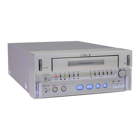
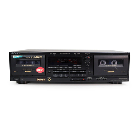
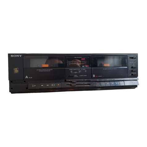
Sony DXA-WZ5 User manual

DXA-WZ5
AEP Model
UK Model
E Model
Australian Model
SERVICE MANUAL
STEREO CASSETTE DECK AMPLIFIER
SPECIFICATIONS
Ver 1.0 2003. 04
•DXA-WZ5 is deck and amplifier
section in MHC-WZ5.
Amplifier section
European model:
DIN power output (rated):75 + 75 watts (6 ohms at
1kHz,DIN)
Continuous RMS power output (reference):
100 + 100 watts (6 ohms
at 1 kHz, 10% THD)
at
at
1kHz, 10% THD)
at 1 kHz, 10% THD)
Music power output (reference):
200 + 200 watts (6 ohms
The following measured at AC 120, 220, 240 V AC,
50/60 Hz (Australian model at 240 V AC, 50/60 Hz)
DIN power output (rated): 100 +100 watts (6 ohms
1kHz, DIN)
Continuous RMS power output (reference):
140 + 140 watts (6 ohms
Inputs
MD (VIDEO) IN (phono jacks):
Voltage 450 mV/250 mV,
impedance 47 kilohms
Outputs
PHONES (stereo mini jack):
Accepts headphones of
8ohms or more
MD (VIDEO) OUT (phono jacks):
Voltage 250 mV,
impedance 1 kilohms
FRONT SPEAKER: Use only the supplied
speaker SS-WZ5/WZ5E
SUB WOOFER (Except for European model):
Voltage 320mV,
impedance 1 kilohms
Tape deck section
Except for European model:
Recording system 4-track 2-channel, stereo
Frequency response 50 – 13,000 Hz (±3 dB),
using Sony TYPE I
cassettes
General
Power requirements
European model: 230 V AC, 50/60 Hz
Australian model: 230 – 240 V AC, 50/60 Hz
TW model: 120 V AC, 50/60 Hz
Other models: 120 V, 220 V or
230 – 240 V AC, 50/60 Hz
Adjustable with voltage
selector
Power consumption
European model: 150 watts
0.3 watts (at the Power
Saving Mode)
Except for European model:
180 watts
Dimensions (w/h/d)
Amplifier/Tape deck:
Amplifier/Tape deck
Approx. 255 ×135 ×
330 mm
Mass
European model: Approx. 6.0 kg
Except for European model:
Approx. 6.3 kg
Design and specifications are subject to change
without notice.
Sony Corporation
Home Audio Company
Published by Sony Engineering Corporation
9-877-330-01
2003D1600-1
© 2003.04
Tape deck
Section Model Name Using Similar Mechanism NEW
Tape Transport Mechanism Type CWM43RR23

2
DXA-WZ5
SAFETY-RELATED COMPONENT WARNING!!
COMPONENTS IDENTIFIED BY MARK 0OR DOTTED LINEWITH
MARK 0ON THE SCHEMATIC DIAGRAMS AND INTHE PARTS
LIST ARE CRITICAL TO SAFE OPERATION. REPLACE THESE
COMPONENTS WITH SONY PARTS WHOSE PART NUMBERS
APPEAR AS SHOWN IN THIS MANUAL OR IN SUPPLEMENTS
PUBLISHED BY SONY.
Notes on chip component replacement
•Never reuse a disconnected chip component.
•Notice that the minus side of a tantalum capacitor may be
damaged by heat.
Flexible Circuit Board Repairing
•Keep the temperature of soldering iron around 270˚C
during repairing.
•Do not touch the soldering iron on the same conductor of the
circuit board (within 3 times).
•Be careful not to apply force on the conductor when soldering
or unsoldering.
TABLE OF CONTENTS
MODEL IDENTIFICATION
— BACK PANEL —
•Abbreviation
AUS:Australian model
E2 : 120V AC Area in E model
E3 : 240V AC Area in E model
KR : Korean model
TW :Taiwan model
PARTS No.
VOLTAGE SELECTOR Switch
Power Voltage Indication
1. GENERAL ·········································································· 3
2. DISASSEMBLY ························································· 5
2-1. Case ··············································································· 5
2-2. Switching Power, DC Fan, Back Panel ························· 6
2-3. MAIN Board ································································· 6
2-4. AMP Board ··································································· 7
2-5. Front Panel Assy ···························································· 7
2-6. Tape mechanism deck (CWM43RR23) ························ 8
2-7. Lid (TC)Assy, Holder (A) Assy, Holder (B)Assy········ 8
3. ELECTRICAL ADJUSTMENTS ································· 9
4. DIAGRAMS······································································ 10
4-1. Block Diagrams - Main Section -································ 11
4-2. Printed Wiring Board - MAIN Board - ······················· 12
4-3. Schematic Diagram - MAIN Board (1/2) - ················· 13
- MAIN Board (2/2) - ················· 14
4-4. Printed Wiring Board - AMP Board -·························· 15
4-5. Schematic Diagram - AMP Board - ····························16
5. EXPLODEDVIEWS
5-1. Front Panel Section ····················································· 17
5-2. Chassis Section ···························································· 18
5-3. Tape Mechanism Deck Section ··································· 19
6. ELECTRICAL PARTS LIST ······································· 20
Unleaded solder
Boards requiring use of unleaded solder are printed with the lead-
free mark (LF) indicating the solder contains no lead.
(Caution: Some printed circuit boards may not come printed with
the lead free mark due to their particular size.)
: LEAD FREE MARK
Unleaded solder has the following characteristics.
•Unleaded solder melts at a temperature about 40°C higher than
ordinary solder.
Ordinary soldering irons can be used but the iron tip has to be
applied to the solder joint for a slightly longer time.
Soldering irons using a temperature regulator should be set to
about 350°C.
Caution: The printed pattern (copper foil) may peel away if the
heated tip is applied for too long, so be careful!
•Strong viscosity
Unleaded solder is more viscous (sticky, less prone to flow) than
ordinary solder so use caution not to let solder bridges occur such
as on IC pins, etc.
•Usable with ordinary solder
It is best to use only unleaded solder but unleaded solder may
also be added to ordinary solder.
[When bringing in the equipment for service]
In case of repairing, please bring the entire system set([HCD-WZ5,
DXA-WZ5],except for the speaker) to the service station.
MODEL
AEP, UK models
E2 model
E3 model
AUS model
KR model
TW model
PARTS No.
4-244-468-0s
4-244-468-1s
4-244-468-1s
4-244-468-3s
4-244-468-9s
4-244-468-8s
POWERVOLTAGE INDICATION
AC:230V 50/60HZ
AC:120V 60HZ
AC:240V 50HZ
AC:230-240V 50/60HZ
AC:220V 50/60HZ
AC:120V 50/60HZ

3
DXA-WZ5
This section is extracted
from instruction manual.
SECTION 1
GENERAL
Main unit
Deck A wh
Deck B wd
A Z(eject) wg (15)
ZB (eject) wf (15)
ALPHABETICAL ORDER
A – L
BUTTON DESCRIPTIONS
Amplifier Tape deck

4
DXA-WZ5
Perform the following procedures 1to 5to hook up your system using the supplied cords and
accessories. Australian model is used for illustration purpose.
Preparation
Place the components as shown below.
1Connect the system control cables to
the SYSTEM CONTROL connectors on
the tape deck.
Connect to the same numbered jack in the
order indicated on the rear panel.
Note
The system cable is used to send signals and electricity
between the components for interlinked operation.
Be sure to insert the connector horizontally until it
clicks into place. Otherwisethe system will notoperate
correctly.
2Connect the speakers.
Connect the speaker cords to the
SPEAKER terminals on the tape deck and
to the terminals on the speakers as shown
below.
Speakers
Getting Started
Hooking up the system
AM loop antenna
Front
speaker (right) Front
speaker (left)
FM lead antenna
Amplifier/
CD player/
Tuner Tape deck
Tape deck CD player/
Tuner
RL
SPEAKER
Gray (3)
Black (#)
Gray (3)
Black (#)
Amplifier/

5
DXA-WZ5
SECTION 2
DISASSEMBLY
•The equipment can be removed using the following procedure.
SET
FRONT PANEL ASSY
LID (TC) ASSY,
HOLDER (A) ASSY,
HOLDER (B) ASSY
CASE
MAIN BOARD
AMP BOARD
TAPE MECHANISM DECK
(CWM43RR23)
SWITCHING POWER,
DC FAN, BACK PANEL
2-1. Case
Note : Follow the disassembly procedure in the numerical order given.
3
three screws
(+BVTP 3
×
8
)
1
two screws
(case 3 TP2)
2
two screws
(case 3 TP2)
4
case

6
DXA-WZ5
2-2. Switching Power, DC Fan, Back Panel
2-3. MAIN Board
1
five screws
(+BVTP 3
×
8)
2
six screws
(+BVTP 3
×
8)
7
two screws
(+BVTP 3
×
8)
9
DC fan
q;
back panel
5
two screws
(+BVTP 3
×
8)
8
connector
(CN204)
3
connector
(CN201)
4
connector
(CN101)
6
switching power
1
three screws
(+BVTP 3
×
8)
4
wire (flat type)
(13 core)
6
connector
(CN301)
8
connector
(CN605)
9
connecto
r
(CN604)
q;
MAIN boar
d
7
connector
(CN102)
5
connector
(CN302)
2
connector
(CN502)
3
connector
(CN501)

7
DXA-WZ5
2-4. AMP Board
2
three screws
(+BVTP 3
×
8)
1
Remove the soldering.
3
AMP board
2-5. Front Panel Assy
8
front panel
assy
1
two screws
(+BVTP 3
×
8)
5
claw
2
wire (flat type)
(13 core)
4
wire
3
screw
(+BVTP 3
×
8)
6
connector
7
connector

8
DXA-WZ5
2-6. Tape mechanism deck (CWM43RR23)
2-7. Lid (TC) Assy, Holder (A) Assy, Holder (B) Assy
1
four screws
(+BVTP 2.6
×
8
)
5
two screws
(+BVTP 2.6
×
8)
4
3
tape
mechanism deck (CWM43RR23)
6
four claws
7
base lock
2
wire
qa
holder (lock)
8
lever (R)
q;
lever (C)
9
lever (L)
qs
button (A)
qd
button (B)
1
spring (lid)
2
spring (lid-R)
3
lid (TC) assy
4
claw
8
claw
5
damper
9
damper
6
spring holder (A)
q;
spring holder (B)
7
holder (A) assy
qa
holder (B) assy

9
DXA-WZ5
SECTION 3
ELECTRICAL ADJUSTMENTS
2. Turn the adjustment screw and check output peaks. If the peaks
do not match for L-CH and R-CH, turn the adjustment screw
so that outputs match within 1dB of peak.
Note: Confirm each contents of this section first of all. If the results are
not satisfied, do the adjustment.
1. Demagnetize the record/playback head with a head
demagnetizer.
2. Do not use a magnetized screwdriver for the adjustments.
3. After the adjustments, apply suitable locking compound to the
parts adjust.
4. The adjustments should be performed with the rated power
supply voltage unless otherwise noted.
5. The adjustments should be performed in the order given in this
service manual.
6. The adjustments should be performed for both L-CH and R-
CH.
7. Switches and controls should be set as follows unless otherwise
specified.
•Test Tape
Record/Playback Head Azimuth Adjustment
Procedure:
1. Mode: Playback
set
SPEAKER terminals (TM402)
L-CH, R-CH
+
–
level meter
test tape
P-4-A63J
(10 kHz, –10 dB)
Screw
position
L-CH
peak
within
1 dB
Output
level
L-CH
peak R-CH
peak
within
1 dB
Screw
position
R-CH
peak
set
test tape
P-4-A63J
(10 kHz, –10 dB)
R-CH
oscilloscope
L-CH
R-CH
VH
waveform of oscilloscope
in phase 45
°
90
°
135
°
180
°
good wrong
SPEAKER terminals (TM402
)
L-CH
3. Mode: Playback
4. Repeat step 1 to 3 in playback (REV) mode.
5. After the adjustments, apply suitable locking compound to the
pats adjusted.
DECK SECTION
Tape Signal Used for
P-4-A63J 10 kHz, –10 dB Azimuth Adjustment
0 dB=0.775 V

10
DXA-WZ5
•WAVEFORMS
SECTION 4
DIAGRAMS
Note on Schematic Diagram:
•All capacitors are in µF unless otherwise noted. pF: µµF
50 WV or less are not indicated except for electrolytics
and tantalums.
•All resistors are in Ωand 1/4W or less unless otherwise
specified.
•¢: internal component.
•2: nonflammable resistor.
•5: fusible resistor.
•C: panel designation.
Note on Printed Wiring Boards:
•X: parts extracted from the component side.
•Y: parts extracted from the conductor side.
•b: Pattern from the side which enables seeing.
•A: B+ Line.
•B: B– Line.
•H: adjustment for repair.
•Voltages and waveforms are dc with respect to ground
under no-signal (detuned) conditions.
•Voltages aretakenwithaVOM(Inputimpedance 10 MΩ).
Voltage variations may be noted due to normal produc-
tion tolerances.
no mark : FM
():CD
[]:TAPE
•Waveforms are taken with a oscilloscope.
Voltage variations may be noted due to normal produc-
tion tolerances.
•Circled numbers refer to waveforms.
•Signal path.
F: FM
E: PB (TAPE)
a: REC (TAPE)
J: CD
•Abbreviation
AUS:Australian model
E2 : 120V AC Area in E model
E3 : 240V AC Area in E model
KR : Korean model
TW :Taiwan model
THIS NOTE IS COMMON FOR PRINTEDWIRING BOARDS AND SCHEMATIC DIAGRAMS.
(In addition to this, the necessary note is printed in each block.)
C
B
These are omitted.
E
Q
B
These are omitted.
CE
Q
11.2
µ
s
15.9 Vp-p
5 V/DIV, 4
µ
s/DIV
1
Q301 collector (TAPE B REC)
–TC MAIN Board –
Note: The components identified by mark 0or dotted line
with mark 0are critical for safety.
Replace only with part number specified.
Caution:
Pattern face side: Partsonthepatternfacesideseen from
(SIDE B) the pattern face are indicated.
Parts face side: Parts on the parts face side seen from
(SIDE A) the parts face are indicated.
•Indication of transistor.

1111
DXA-WZ5
4-1. Block Diagrams – Main Section –
: REC (TAPE)
: FM
: CD
• Signal Path
• R-CH is omitted due to same as L-CH.
TAPE DECK
BLOCK
PB L
MAIN TRANS
RELAY
DRIVE
Q601 RY601
AC
IN
PB R
A SHUT
B SHUT
R-CH
REC L
REC R R-CH
GND
MUTE
CONT
JW603
RY402
14
15
12
9
8
POWER AMP
IC501
Q536,537
52
IC301
1
BIAS 8
7
16
5
67
IC303
CNT BIAS
REC SWITCH
Q312,314
REC CONT
Q308-310
PB SWITCH
Q303
PB CONT
Q306,307
BIAS
OSC
Q304
T301
BIAS
E HOT
BIAS
SWITCH
Q301
BIAS
CONT
Q305
BIAS
21
I/O EXP DATA OUT
I/O EXPANDER
I/O EXP DATA IN
I/O EXP CLK
I/O EXP LAT
A TRG
UNREG
EVER +4V
CN CHECK
AMP+9V AMP+9V
M+9V
REC-L
REC-R
PB-R
PB-L
B SHUT
A SHUT
R-CH
R-CH
B TRG
IC251
A/B
23
20
FR RY
11
PROTECT
REC/PB
22
A PLAY
B PLAY
A HALF
B HALF
REC(FWD)
REC (REW)
CAP M+
MOTOR
DRIVE
Q353,356
A TRG A T SOL
Q351,355
B TRG B T SOL
Q352,354
A PLAY
5
B PLAY
9
A HALF
6
B HALF
8
REC(FWD)
7
REC(REW)
10
CAP-M
24
HCD-WZ5
31
4
IC201
PROTECTOR
25
DO
26
DI
3
CLK
4
LATCH
MUTE
Q533
MUTE
CONT
Q204,206
MUTE
Q501
R-CH
L
R
TM402
SPEAKER
FAN301
FAN
DRIVE
Q209,211,212
PROTECT
SWITCH
Q536,537 +VL
TH531
OVER HEAT
DETECTOR
17
PWR RY
D501
Q521
Q534,535
PROTECT
DETECTOR
Q403
RELAY
DRIVE
D101
+9V
REG 1
3
IC302
+VL
D103 AC3
AC3
D301
R-CH
D402
+3.3V
REG
Q101
D+3.3V
Q202
D202
D201
AC
DET
Q203,205
M+9V
-VL
AC2
AUS
E2, E3
KR
AEP, UK, TW
AC2
+VH
-VH
AC1
AC1
D102
: PB (TAPE)
D251
IC251
VCC
DBFB FB
STK MUTE
STK MUTE
FRONT-R
FRONT-L
JW603
JW603
S601
VOLTAGE
SELECTOR
SWITCHING
REGULATOR
EVER+4V

1212
DXA-WZ5
4-2. PrintedWiring Board – MAIN Board –
IC301
IC303
IC201
IC302
IC251
TWKR
/ WZ5E
1
13
216
15
3
1
C310
• : Uses unleaded solder.
• Semiconductor
Location
Ref. No. Location
D101 C-9
D102 B-7
D103 A-7
D111 A-6
D201 I-4
D202 I-4
D204 F-2
D205 E-2
D207 E-3
D208 E-3
D209 F-1
D251 G-3
D301 B-6
D351 E-5
D352 E-5
D402 G-3
D404 H-3
D911 C-2
IC201 I-4
IC251 F-4
IC301 I-10
IC302 A-7
IC303 J-8
Q101 A-6
Q202 I-5
Q203 I-5
Q204 E-2
Q205 I-5
Q206 E-2
Q209 E-2
Q211 F-2
Q212 F-2
Q301 F-9
Q302 H-10
Q303 H-9
Q304 G-8
Q305 F-8
Q306 H-8
Q307 H-9
Q308 H-8
Q309 H-8
Q310 H-8
Q311 G-9
Q312 G-9
Q313 G-9
Q314 G-9
Q351 E-5
Q352 E-5
Q353 E-5
Q354 E-4
Q355 E-4
Q356 E-4
Q403 H-4
Q601 C-2

1313
DXA-WZ5
4-3. Schematic Diagram – MAIN Board (1/2) – • See page 10 forWaveforms.
C107
C108
D103
R103
R104
C111
C112
D102
C251
C320
C319
R315
C312
C302
C351
R352
C352
R351
R353
R358
R359
R360
R366
R365
R364
R363
R362
R361
R367
R368
D351
D352
C305
C318
C308
C118
C120
C303
C317
R263
R264
R328
R329
R369
R370
C114
IC302
R330
C327 C328
L302
L303
L304
C330
C304
C315
F102
F101
F103
F104
F105
R308
C309
C333
C334
C337
R343
R344
R204
R201
R203
R254
R252R251
R253
R256
R257
R258
R259
R260
C252
R316
R322 R324
R321 R323
C322C321
R311
R307
R305
R320
R318
R314
T301
R354
R355
R357
R356
C316
C307
C311
R319R317
R261
R262
R255
R128
D111
R325
C323
C353
C354
C324
C253
R334
IC301
R303
R304
R306
R310
R309
R335
R338
R336
C313
C255
R340
C326
R341
C331
CN351
C301
C314
R312
R302
R313 C329
C332
R327R326
R331
CN302
CN301
C105
C106
C338
C325 R339
R337
Q312
Q314
Q313
Q311
Q310
Q308
Q309
Q306
Q307
Q303
Q302
Q304
Q305
C306
Q352
Q301
Q354
Q355
Q356
Q353Q351
IC251
Q101
C113
D301
CN102
D101
C103
C104
C109
C110
IC303
D251
FH101 FH151
FH103 FH153
FH102 FH152
JW394
FH105 FH155
FH104 FH154
0.01
0.01
D3SBA20
100k
100k
D5SBA20
0.01
2200p
2200p
4.7k
0.01
0.0047
0.0047
680
0.0047
680
47k
3.3k
3.3k
3.3k
10k
10k
10k
10k
10k
10k
10k
10k
1SS355
1SS355
680p
680p
22
50V
10
50V
10
50V
680p
680p
10k
10k
2.2k
2.2k
100
100
0.01
TA7809S
22k
680p 680p
27mH
27mH
100p
0.01
C310
0.1
0.01
100
100
10V
4700p
4700p
330p
33k
33k
100k
4.7k
4.7k
100
100100
100
100
100
100
100
100
10
50V
8.2k
1k
1k
1k 1k
0.0010.001
10
10k
47
4.7k
4.7k
47k
2.2k
2.2k
2.2k
2.2k
0.47
50V
0.47
50V
220
10V
10k10k
100
100
100
1k
UDZSTE-173.9B
10k
1
50V
470
16V
10
50V
10
50V
0.1
6.8k
BA3402
330k
12k
100
12k
330k
33k
33k
100
22
50V
470p
220
100 10V
220
4.7 50V
13P
0.01
0.0068
33
3.3k
8.2k 100p
4.7
50V
10015k
22k
8P
3P
0.1
0.1
330p
10 50V 100
6.8k
2SC3624A -T1L15L16
2SC3624A -T1L15L16
2SC3624A
-T1L15L16
2SC3624A
-T1L15L16
2SA812-T1-M5M6
DTC114EKA-T146
DTC114EKA-T146
DTC114EKA-T146
DTA114EKA-T146
2SC3624A
-T1L15L16
2SC3624A
-T1L15L16
RT1P137L-TP
DTC114EKA-T146
47
16V
2SB1116-TP-LK
2SC2001-TP-LK
DTC114EKA
-T146
DTC114EKA
-T146
DTC114EKA
-T146
2SB1116-TP-LK2SB1116-TP-LK
PT8300R-TP
2SC1623-T1-L5L6
25V
10EDB40-TB3
7P
P3SBA20-4101
50V
50V
NJM4580V(TE2)
1SS355
TE-17
*
*
*
*
*
*
*

1414
DXA-WZ5
– MAIN Board (2/2) –
KR TW
C209
C207
C205
C201
R432
R433
L404
R428
L403
R427
C413
C414
R414
R419
R401
R403
C211
R217
R221
R220
C206
C210
C208
R219
R218
IC201
R209
C216
R207
R202
R410
R206
R205
C202
C203
C402 C407
C405 C408
JW124
JW123
R411
R422
R413 R415
R216
R210
R211
R212
CN204
R423
NO1
D911
Q601
C603
R601
L601
C601
C602
JW610
FH651 F601 FH601
JW602
JW612 JW611
JW604
JW603
S601
CN604
NO802
D201
D202
C204
Q204
Q206
D208D205
D207
Q209
R213
Q211
Q212
Q203
Q202
Q205
D204
D209
CN205
D402
D404
Q403
RY402
NO702
R417
CN206
JW101
CN605
CN602
RY601
JW108
TM402
100
10V
10
50V
100
10V
10
50V
0.01
0.01
2.2k 10k
68k
47k
4.7
50V
22k
4.7k
47k
0.01
47
16V
0.01
22k
100
RT8H015C
100
0.01
4.7k
2.2k
100k
10k
22k
10
50V
10
50V
100
1W
47k
22k 22k
220k
1k
1k
1k
3P
47k
WIRE
1SS355
2SC1623
0.01
4.7k
0.1
0.1
2P
7P
1SS355
TE-17 1SS355
TE-17
10
50V
DTA114EKA
-T146
DTC114EKA
-T146
10EDB40-TB310EDB40-TB3
10EDB40-TB3
2SD2525(TP)
0
2SC1623
-T1-L5L6 2SC1623
-T1-L5L6
2SC1623
-T1-L5L6
2SC1623
-T1-L5L6
2SC1623
-TI-L5L6
UDZSTE-1713B
1SS355-17
15P
1SS355-17
1SS355-17
2SC1623
-T1-L5L6
RELAY
12V
8P
4.7k
17P
2P
*
*
*
*
*
*
**
**
*
*
*2
*2 *2 *2
*2
*2 *2
*2
*2
*2
*2

1515
DXA-WZ5
4-4. PrintedWiring Board – AMP Board –
IC501
Q531
• : Uses unleaded solder.
• Semiconductor
Location
Ref. No. Location
D501 D-3
D504 A-1
D505 A-1
D521 C-2
D532 D-2
D571 C-2
IC501 A-2
Q501 C-4
Q521 B-2
Q531 D-2
Q533 C-2
Q534 D-3
Q535 D-3
Q536 C-3
Q537 C-3
Q551 C-4
Q571 B-2

1616
DXA-WZ5
4-5. Schematic Diagram – AMP Board –
R510
R524
R574
C502
C552
R501
R502
R504
R505
R523
R555
R573
R526
R539
R543
R545
R547
R548
R551
R552
R554
R535
R537
R500
R540
R536
R576
C571
C572
R571 R521
C522 C521
IC501
C508
R530
TH531 R534
R542
R525
R575
R503
R553
R507
R557
D504
D505
JR501
R546
R541
R544
Q533
CN502
CN501
R572
C551
Q551
Q501
C501
R506
C503
C553
R556
C554 C504
D571
D521
D501
Q571
Q521
C531 C532
C533 C534
D532
Q537
Q535
Q534
R522
Q536
R531
33k
10
1/2W
10
1/2W
470p
470p
2.2k
100k
1k
47k
47k
47k
47k
15k
33k
68k
2.2k
R538
JR502
470k
2.2k
2.2k
2.2k
100k
1k
22
1/4W
FR
22
1/4W
FR
10k
100k
100k
15k
100000p
100000p
1k 1k
100000p 100000p
0.001
100 47k
100k
150k
150k
10k
10k
10k
10k
UDZS-TE-17-13B
UDZS-TE-17-13B
47k
47k
100k
2SC2713G-TE85L
8P
7P
0.22
50V
2SC3624A
-T1L15L16
2SC3624A
-T1L15L16
50V
330
16V
16V
330
100p 100p
1SS355 TE-17
1SS355 TE-17
1SS355 TE-17
2SC1841
TP-PAFAFA
2SC1841
TP-PAFAFA
100V 100V
50V 50V
1SS355
TE-17
2SC1623
-T1-L5L6
2SC1623 -T1-L5L6
2SC1623
Q531
2SC1623
-T1-L5L6
0.22
2SA1163G-TE85L
1
1/4W
RF
*

SECTION 5
EXPLODEDVIEWS
NOTE:
•-XX, -X mean standardized parts, so they may
have some differences from the original one.
•Items marked “*” are not stocked since they
are seldom required for routine service. Some
delayshould beanticipatedwhen orderingthese
items.
•Themechanical partswith noreference number
in the exploded views are not supplied.
•Hardware (# mark) list and accessories and
packing materials are given in the last of this
parts list.
•Abbreviation
AUS:Australian model
E2 : 120V ACArea in E model
E3 : 240V ACArea in E model
KR : Korean model
TW : Taiwan model
17
DXA-WZ5
The components identified by mark 0or
dotted line with mark 0are critical for safety.
Replace only with part number specified.
5-1. Front Panel Section
Ref. No. Part No. Description Remarks Ref. No. Part No. Description Remarks
a
a
e
e
cc
b
b
910
10
13
13
13
13
11
1516
19 20
19
12
22
1417
18
21
not supplied
not supplied
d
d
6
Chassis section
13
4
5
7
8
2
Mechanism deck section
#1
#1
#1
23
14-244-459-01 SPRING (LID-L)
2X-4955-286-1 LID (TC) ASSY
34-244-977-01 SPRING (LID-R)
4X-4955-284-1 HOLDER (A) ASSY
54-244-454-01 SPRING (HOLDER A)
61-769-985-11 WIRE (FLAT TYPE) (13CORE)
7X-4955-285-1 HOLDER (B) ASSY
84-244-455-01 SPRING (HOLDER B)
94-244-442-01 PANEL (TC), FRONT
10 4-224-104-11 DAMPER
11 4-244-443-01 BUTTON (A)
12 4-244-444-01 BUTTON (B)
13 4-951-620-01 SCREW (2.6X8), +BVTP
14 4-244-450-01 HOLDER (LOCK)
15 4-244-448-01 LEVER (L)
16 4-244-447-01 LEVER (C)
17 4-244-449-01 LEVER (R)
18 4-244-446-01 BASE (LOCK)
19 3-363-099-11 SCREW (CASE 3 TP2)
20 4-244-441-11 CASE
21 4-245-758-01 PLATE (HEAD), SHIELD
22 7-685-853-04 SCREW +BVTT 2X6 (S)
23 7-685-862-09 SCREW +BVTT 2.6X6 (S)
#1 7-685-646-79 SCREW +BVTP 3X8 TYPE2 IT-3

18
DXA-WZ5
5-2. Chassis Section
Ref. No. Part No. Description Remarks Ref. No. Part No. Description Remarks
a
a
not supplied
not supplied
not supplied
not supplied
not supplied
not supplie
d
not
supplied
#1
#1
#1
#1
#1
#1
#1
#1
#1
#1
#2
#1
#1
#1
not supplied
not supplied
51
52
53
53
58
58
58
55
56
59
60
54
57
F105 F601
F101
T302
FAN301
F102
F103
F104
51 A-4731-824-A AMP BOARD, COMPLETE (AEP,UK)
51 A-4731-831-A AMP BOARD, COMPLETE (E2,E3,KR,TW,AUS)
52 A-4731-819-A MAIN BOARD, COMPLETE (AEP,UK)
52 A-4731-828-A MAIN BAORD, COMPLETE (E3,TW)
52 A-4733-378-A MAIN BOARD, COMPLETE (E2)
52 A-4733-381-A MAIN BOARD, COMPLETE (AUS)
52 A-4748-134-A MAIN BOARD, COMPLETE (KR)
53 4-900-386-01 SCREW
54 3-703-571-11 BUSHING (S) (4516), CORD (E2,E3,KR,TW)
*54 3-703-244-00 BUSHING (2104), CORD (AEP,UK,AUS)
055 1-468-737-11 POWER, SWITCHING
056 1-696-845-11 CORD, POWER (AUS)
056 1-751-523-11 CORD, POWER (UK)
056 1-777-071-63 CORD, POWER (AEP)
056 1-783-820-21 CORD, POWER (TW)
056 1-791-169-11 CORD, POWER (KR)
056 1-827-226-21 CORD, POWER (E2,E3)
057 1-569-007-11 ADAPTOR, CONVERSION (E3)
58 3-970-608-01 SUMITITE (B3), +BV
59 1-500-386-11 FILTER, CLAMP (FERRITE CORE)
60 3-655-653-21 BAND (TAITON), BINDING
0F101 1-533-473-11 FUSE, GLASS TUBE (DIA. 5) (6.3A/250V)
0F102 1-533-473-11 FUSE, GLASS TUBE (DIA. 5) (6.3A/250V)
0F103 1-533-473-11 FUSE, GLASS TUBE (DIA. 5) (6.3A/250V)
0F104 1-533-473-11 FUSE, GLASS TUBE (DIA. 5) (6.3A/250V)
0F105 1-533-471-11 FUSE, GLASS TUBE (DIA. 5) (4A/250V)
0F601 1-533-471-11 FUSE, GLASS TUBE (DIA.5) (4A/250V)
(E2,E3,KR,TW)
FAN301 1-763-072-11 FAN, DC
0T302 1-439-597-11 TRANSFORMER, POWER (AEP,UK)
0T302 1-439-598-11 TRANSFORMER, POWER (E2,E3,KR,TW,AUS)
#1 7-685-646-79 SCREW +BVTP 3X8 TYPE2 IT-3
#2 7-685-650-79 SCREW +BVTP 3X16 TYPE2 IT-3
The components identified by mark 0or
dotted line with mark 0are critical for safety.
Replace only with part number specified.

19
DXA-WZ5
5-3.Tape Mechanism Deck Section
Ref. No. Part No. Description Remarks Ref. No. Part No. Description Remarks
101
102
103
104
not supplied
not supplied
not supplied
not supplied
101 1-796-487-31 DECK, MECHANICAL
102 4-243-610-01 BELT (AL)
103 4-243-609-01 BELT (AF)
104 4-243-608-01 BELT (BR)

20
DXA-WZ5 SECTION 6
ELECTRICAL PARTS LIST
NOTE:
•Due to standardization, replacements in the
parts list may be different from the parts
specifiedin thediagramsor thecomponents
used on the set.
•-XX, -X mean standardized parts, so they
may have some difference from the original
one.
•RESISTORS
All resistors are in ohms.
METAL: metal-film resistor
METAL OXIDE: Metal Oxide-film resistor
F: nonflammable
•Items marked “*” are not stocked since they
are seldom required for routine service. Some
delayshould beanticipatedwhen orderingthese
items.
•Abbreviation
AUS:Australian model
E2 : 120V ACArea in E model
E3 : 240V ACArea in E model
KR : Korean model
TW : Taiwan model
•CAPACITORS:
uF: µF
•COILS
uH: µH
•SEMICONDUCTORS
In each case, u: µ, for example:
uA...: µA... , uPA... , µPA... ,
uPB... , µPB... , uPC... , µPC... ,
uPD..., µPD...
When indicating parts by reference number,
please include the board name.
The components identified by mark 0or
dotted line with mark 0are critical for safety.
Replace only with part number specified.
A-4731-824-A AMP BOARD, COMPLETE (AEP,UK)
A-4731-831-A AMP BOARD, COMPLETE (E2,E3,KR,TW,AUS)
********************
< CAPACITOR >
C501 1-126-964-11 ELECT 10uF 20.00% 50V
C502 1-162-962-11 CERAMIC CHIP 470pF 10% 50V
C503 1-126-947-11 ELECT 47uF 20.00% 16V
C504 1-162-927-11 CERAMIC CHIP 100pF 5% 50V
C508 1-162-964-11 CERAMIC CHIP 0.001uF 10% 50V
C521 1-131-992-91 CERAMIC CHIP 100000pF 35V
C522 1-131-992-91 CERAMIC CHIP 100000pF 35V
C531 1-128-560-11 ELECT 22uF 20.00% 100V
C532 1-128-560-11 ELECT 22uF 20.00% 100V
C533 1-126-967-11 ELECT 47uF 20.00% 50V
C534 1-128-562-11 ELECT 47uF 20.00% 100V
C551 1-126-964-11 ELECT 10uF 20.00% 50V
C552 1-162-962-11 CERAMIC CHIP 470pF 10% 50V
C553 1-126-947-11 ELECT 47uF 20.00% 16V
C554 1-162-927-11 CERAMIC CHIP 100pF 5% 50V
C571 1-131-992-91 CERAMIC CHIP 100000pF 35V
C572 1-131-992-91 CERAMIC CHIP 100000pF 35V
< CONNECTOR >
*CN501 1-506-486-11 PIN, CONNECTOR 7P
*CN502 1-564-523-11 PLUG, CONNECTOR 8P
< DIODE >
D501 8-719-988-61 DIODE 1SS355TE-17
D504 8-719-083-63 DIODE UDZSTE-1713B
D505 8-719-083-63 DIODE UDZSTE-1713B
D521 8-719-988-61 DIODE 1SS355TE-17
D532 8-719-988-61 DIODE 1SS355TE-17
D571 8-719-988-61 DIODE 1SS355TE-17
< GROUND TERMINAL >
EP502 1-537-738-21 TERMINAL, GROUND
< IC >
IC501 6-600-179-01 IC STK412-210 (AEP,UK)
IC501 6-600-171-01 IC STK412-230 (E2,E3,KR,TW,AUS)
< JUMPER RESISTOR >
JR501 1-216-864-11 METAL CHIP 0 5% 1/16W
< TRANSISTOR >
Q501 8-729-141-73 TRANSISTOR 2SC3624A-T1L15L16
Q521 8-729-140-84 TRANSISTOR 2SC1841TP-PAFAEA
Q533 8-729-271-31 TRANSISTOR 2SC2713G-TE85L
Q534 8-729-120-28 TRANSISTOR 2SC1623-T1-L5L6
Q535 8-729-120-28 TRANSISTOR 2SC1623-T1-L5L6
Q536 8-729-216-31 TRANSISTOR 2SA1163G-TE85L
Q537 8-729-120-28 TRANSISTOR 2SC1623-T1-L5L6
Q551 8-729-141-73 TRANSISTOR 2SC3624A-T1L15L16
Q571 8-729-140-84 TRANSISTOR 2SC1841TP-PAFAEA
< RESISTOR >
R500 1-216-833-11 METAL CHIP 10K 5% 1/16W
R501 1-216-825-11 METAL CHIP 2.2K 5% 1/16W
R502 1-216-845-11 METAL CHIP 100K 5% 1/16W
R503 1-216-833-11 METAL CHIP 10K 5% 1/16W
R504 1-216-821-11 METAL CHIP 1K 5% 1/16W
R505 1-216-841-11 METAL CHIP 47K 5% 1/16W
R506 1-216-815-11 METAL CHIP 330 5% 1/16W
R507 1-216-833-11 METAL CHIP 10K 5% 1/16W
R510 1-216-839-11 METAL CHIP 33K 5% 1/16W
R521 1-216-821-11 METAL CHIP 1K 5% 1/16W
0R522 1-220-894-11 METAL 0.22 10% 5W
R523 1-216-841-11 METAL CHIP 47K 5% 1/16W
R524 1-249-625-31 CARBON 10 5% 1/2W
R525 1-216-847-11 METAL CHIP 150K 5% 1/16W
R526 1-216-835-11 METAL CHIP 15K 5% 1/16W
R530 1-216-809-11 METAL CHIP 100 5% 1/16W
0R531 1-217-637-00 FUSIBLE 1 5% 1/4W
R534 1-216-841-11 METAL CHIP 47K 5% 1/16W
0R535 1-219-786-11 FUSIBLE 22 5% 1/4W
0R537 1-219-786-11 FUSIBLE 22 5% 1/4W
R539 1-216-839-11 METAL CHIP 33K 5% 1/16W
R540 1-216-845-11 METAL CHIP 100K 5% 1/16W
R541 1-216-841-11 METAL CHIP 47K 5% 1/16W
R542 1-216-845-11 METAL CHIP 100K 5% 1/16W
R543 1-216-843-11 METAL CHIP 68K 5% 1/16W
R544 1-216-845-11 METAL CHIP 100K 5% 1/16W
R545 1-216-825-11 METAL CHIP 2.2K 5% 1/16W
R546 1-216-841-11 METAL CHIP 47K 5% 1/16W
R547 1-216-825-11 METAL CHIP 2.2K 5% 1/16W
R548 1-216-825-11 METAL CHIP 2.2K 5% 1/16W
R551 1-216-825-11 METAL CHIP 2.2K 5% 1/16W
R552 1-216-845-11 METAL CHIP 100K 5% 1/16W
R553 1-216-833-11 METAL CHIP 10K 5% 1/16W
R554 1-216-821-11 METAL CHIP 1K 5% 1/16W
AMP
Ref. No. Part No. Description Remarks Ref. No. Part No. Description Remarks
Table of contents
Other Sony Cassette Player manuals

Sony
Sony CFD-515 User manual

Sony
Sony Walkman WM-D6C User manual

Sony
Sony XR-CA600X - Fm/mw/sw Cassette Car Stereo User manual

Sony
Sony TC-WE435 User manual

Sony
Sony Walkman WM-FX465 User manual

Sony
Sony WM-10II User manual

Sony
Sony Pressman TCM-16 User manual

Sony
Sony CFS-616S User manual

Sony
Sony TC-K370 User manual

Sony
Sony J10 User manual

Sony
Sony Walkman WM-GX788 User manual

Sony
Sony TCM-459V User manual

Sony
Sony Walkman WM-FX355 User manual

Sony
Sony WALKMAN WM-702 User manual

Sony
Sony CFM-104 Marketing User manual

Sony
Sony Walkman WM-EX651 User manual

Sony
Sony EV-S350 User manual

Sony
Sony CFD-S23 User manual

Sony
Sony TC-K808ES User manual

Sony
Sony WM-FX197 Marketing User manual